Abstract
A novel vertical translational microactuator based on thin-film piezoelectric actuation is presented, using a set of four compound bend-up/bend-down unimorphs to produce translational motion of a moving platform or stage. The actuation material is a chemical-solution deposited lead–zirconate–titanate (PZT) thin film. Prototype designs have shown as much as 120 μm of static displacement, with 80–90 μm displacements being typical, using four 920 μm long by 70 μm legs. Analytical models are presented that accurately describe nonlinear behavior in both static and dynamic operation of prototype stages when the dependence of piezoelectric coefficients on voltage is known. Resonance of the system is observed at a frequency of 200 Hz. The large displacement and high bandwidth of the actuators at low-voltage and low-power levels should make them useful to a variety of optical applications, including endoscopic microscopy.
1. Introduction
Design, testing and analysis of a large displacement, vertical translational actuator based on lead–zirconate–titanate (PZT) thin films is presented. While a variety of vertical translational actuators have been demonstrated using microelectromechanical system (MEMS) technology, thin-film piezoelectric materials have the capacity to produce actuation with especially large displacements with low power and high speeds. Unlike electrostatic actuation, vertical actuation based on elastic deformation of thin-film piezoelectric structures is not limited by gap distances between electrodes. Meanwhile, piezoelectric actuation typically consumes far less power than electrothermal actuation, and allows for a greater degree of process integration than most electromagnetic or hydraulic actuators.
The vertical actuator to be discussed is based on a PZT thin film and has demonstrated up to 120 μm of static displacement at 20 V, while being integrated with larger silicon microstructures. The actuator has sufficient speed for a variety of optical instrument applications, with the immediate application motivating device design being into-tissue scanning of a dual-axes confocal endoscopic microscope [1]. In such a system, a scanning mirror must be translated parallel to the optical path, with large displacement, small footprint (<5 mm diameter) and minimal thickness. The ability to provide large vertical translations from the surface of a silicon wafer allows for a very compact actuator design. Translational actuation is realized through a combination of unimorph piezoelectric cantilevers arranged as legs around a central moving platform, or stage, as shown in figure 1. Each leg consists of a bend-up and a bend-down unimorph segment, shown schematically in figure 2. Combining the bend-up/bend-down structure with symmetry from the legs arranged around the stage produces a net translational motion of the silicon platform when an electric field is applied across the piezoelectric film.
Figure 1.
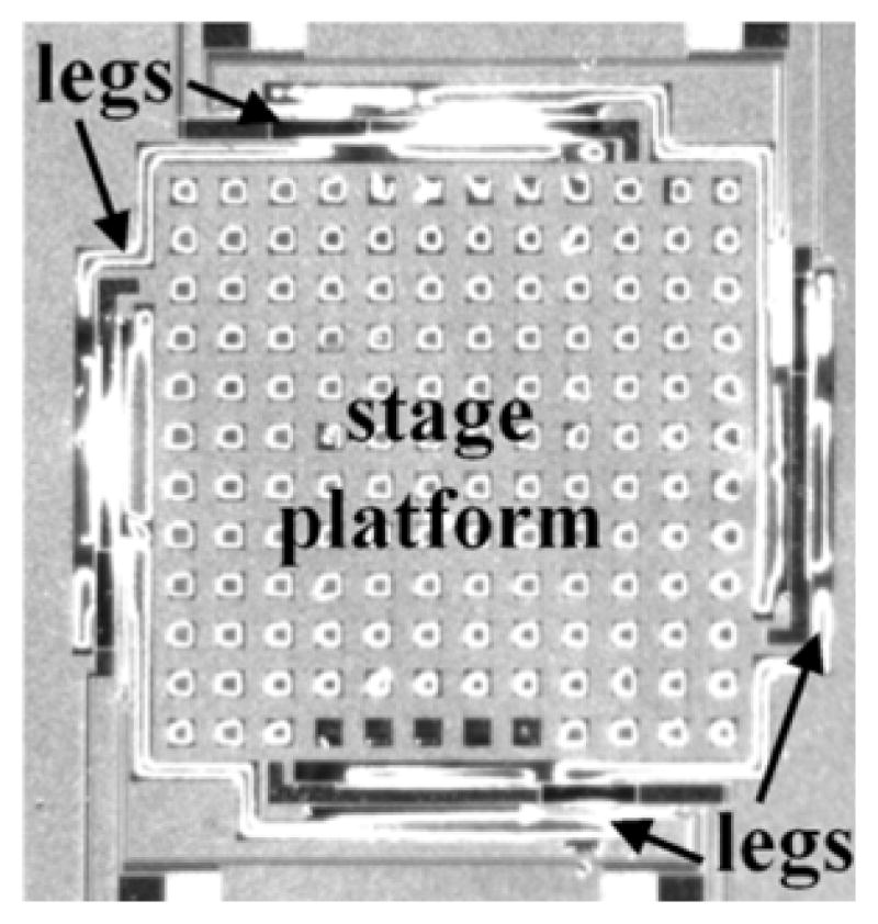
Top-view, piezoelectrically actuated vertical stage.
Figure 2.
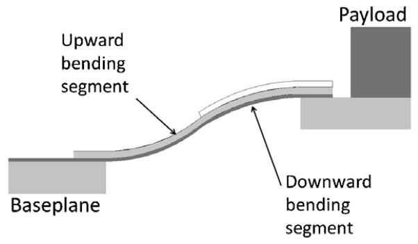
Schematic cross-section of a vertical translational stage.
Previous miniature, vertical actuators with a stroke length greater than 100 μm and footprint within a 5 mm diameter have been based on other actuation mechanisms. Thermal actuators consisting of four electrothermally actuated bimorphs have been demonstrated with several hundred microns of displacement [2, 3], but thermal time constants are comparatively long and power consumption exceeds 100 mW, resulting in temperatures of several hundred degrees celsius; this heat generation would be difficult to dissipate in certain circumstances, such as in vivo endoscopy. Other in-plane and non-translational out-of-plane electrothermal microactuators have also been demonstrated [3–5]. Meanwhile, an electromagnetic actuator has achieved large displacements with minimal heat dissipation, but the coil needed to implement the existing design would obstruct the optical path in a dual-axes confocal microscopy application [6]. In addition, a few linear actuators based on conventional electromagnetic or piezoelectric machining have very small diameters [7–9], but these actuators have lengths of 6 mm or larger, which increases the necessary size of the final optical probe, and would prevent back-loading of the optical system into many endoscopes. Micro-scale hydraulic and pneumatic actuators have also been demonstrated, but require external fluid or air inputs [10–12]. Meanwhile, electrostatic actuators are widely used in microdevices [13–18], but the application of electrostatic actuation methods in biomedical devices is constrained by limitations such as relatively weak force, short stroke (<100 μm) and high operating voltage. For example, Helmbrecht et al have developed vertical actuated MEMS mirrors for adaptive optics based on electrostatic electrode driving, which can perform only 7 μm at high voltage (60 V) [13].
The thin-film PZT actuator described here, referred to as a vertical stage in this paper, overcomes many of these limitations. The actuator operates at low power, can be fabricated from a single integrated process and has a resulting total thickness of just a single silicon wafer, or smaller with wafer thinning prior to release. Large movements from piezoelectric cantilever beams are well known [19, 20], and the configuration developed here allows the vertical motion to be produced with a net translational tip displacement. We have developed both static and dynamic models to predict actuator behavior, and validated these models and actuator operation with prototype z-stages, provided some knowledge of piezoelectric and damping coefficients is available.
This paper is arranged as follows. After this introduction, section 2 describes the actuator geometry and static actuator modeling and design. Section 3 describes the fabrication process for prototype z-stages. Section 4 includes experimental measurements of static and dynamic actuator motion. Section 5 analyzes nonlinear effects on actuator motion, to better explain frequency response measurements. Section 6 discusses advantages and limitations of the design, and implications of these results for device operation in a dual-axes confocal microscope and other optical MEMS devices. Section 7 concludes this paper.
2. Design and static modeling
Vertical motion is typically generated from thin-film piezoelectric materials by managing electrode and other structural layers to place the neutral axis of a piezoelectric unimorph above or below the mid-plane of the piezoelectric film. The z-stage examined here utilizes a silicon dioxide elastic layer to improve thin-film PZT properties, along with platinum electrodes on the top and bottom surfaces of the PZT film. The presence of silicon dioxide at the bottom of the stack lowers the neutral axis of the unimorph, producing a nominal upward bending motion.
To produce a net translational vertical motion at the tip of the unimorph, a portion of the beam is coated with an extra gold layer to produce a downward-bending motion. Combined with symmetry constraints induced by connecting four such actuators to the corners of a square platform, a purely translational motion may be produced if actuator dimensions are identical. The downward-bending effect could also be achieved passively using just the silicon dioxide layer, without any piezoelectric film, but the gold coating on the second segment of the beam also significantly increases the robustness of an actuator against fracture and stiffens the overall system, increasing natural frequency.
A free-body diagram of the upward-bending and downward-bending vertical actuator segments is shown in figure 3. Under a static displacement with no external load, bending results from the combination of applied and reaction moments, allowing simple calculations of displacement even under large deflections. The bend-up (segment 1) and the bend-down (segment 2) segments of the actuators consist of a stack of silicon dioxide, the metal layers and PZT thin film, having composite flexural rigidity (EI)comp1 and (EI)comp2, and neutral axes ȳ1 and ȳ2, respectively. Under an applied voltage, V, the PZT film imparts a bending moment, Mact,
Figure 3.
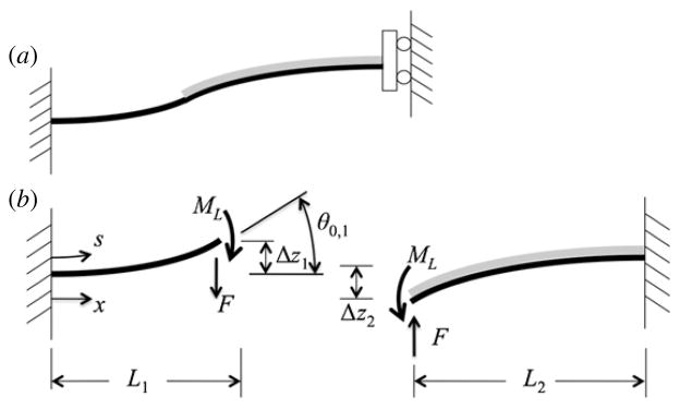
(a) Schematic diagram of a thin-film lateral actuator beam (side views); (b) free-body diagrams used for analysis.
| (1) |
where e31,eff is an effective electroactive piezoelectric stress constant, tPZT is the thickness of the PZT layer, APZT is the cross-sectional area of the PZT layer and ȳPZT is the midline of the PZT film, as measured from the same arbitrary reference as used to define the neutral axis.
It is important to recognize that e31,eff as used in the equations above is an effective electro-active stress constant measuring ratio of stress to electric field, rather than an exact linear piezoelectric constant of the material. The magnitude of e31,eff is determined experimentally by measuring free out-of-plane deflection of cantilever test structures. Alternatively, analysis may sometimes more conveniently be performed using an effective electro-active piezoelectric strain coefficient, d31,eff, given approximately by
| (2) |
where EPZT,nom is a nominal (short circuit) axial elastic modulus of the PZT film in a free beam. The measured values for e31,eff and d31,eff account for a number of effects including the mechanism commonly associated with the term ‘effective piezoelectric coefficient’, d31,f, or ‘effective piezoelectric stress coefficient’, e31,f, as well as nonlinear piezoelectric/ferroelectric and electroactive material responses. The later effects occur because the typical operating fields with these MEMS-scale piezoelectric layers exceed the material’s coercive field. These fields are also in excess of the ‘Rayleigh region’ where properties linearly follow the field and lend themselves to simple analytical models [21]. The axial strain within the piezoelectric layer of the cantilever (zero longitudinal stress) is due to e31,f, according to the elastic coupling
| (3) |
between e33, the true longitudinal piezoelectric stress constant, e31, the in-plane stress constant, and and are the elastic constants at a given electric field [22]. Because the effective electro-active strain coefficient, e31,eff, dictates the behavior of the actuators, this measurable quantity (evaluated from several cantilever beams of varying lengths on each wafer) can provide accurate predictions of actuator behavior. The resulting value of the effective electro-active strain constant, d31,eff, will appear larger than the true linear piezoelectric coefficient of the PZT film, and the magnitude can be very sensitive to processing conditions, varying from wafer to wafer.
Using d31,eff in (1) and grouping the constants in (1) into a moment gain factor, Mcoef, allows the actuation moment to be written as a direct function of the piezoelectric coefficient and voltage:
| (4) |
A summary of the layer thicknesses used in analysis, the estimated elastic moduli from dedicated material testing by Sharpe et al [23, 24] and resulting composite moduli and moment coefficients for beams with width, w, of 70 μm are shown in tables 1 and 2, and will be treated as the nominal values for analysis unless noted otherwise. Also included is the estimated mass of the platform, for a prototype platform dimension of 1.7 mm, fabricated from a 10 μm thick silicon device layer.
Table 1.
Material stack thicknesses and estimated properties.
| Material | Thickness (μm) | Elastic modulus (GPa) |
|---|---|---|
| Silicon oxide | 0.28 | 80 |
| Bottom Ti/Pt | 0.08 | 170 |
| PZT | 0.80 | 70 |
| Top platinum | 0.105 | 170 |
| Titanium/Gold | 1.0 | 86 |
Table 2.
Constant beam parameters.
| Quantity | Units | Estimate |
|---|---|---|
| Mcoef,1 | N m | 0.082 |
| Mcoef,2 | N m | 1.9 |
| (EI)comp,1 | N m2 | 1.1 × 10⁻¹² |
| (EI)comp,2 | N m2 | 5.5 × 10⁻¹² |
| ȳ1 | μm | 0.02 |
| ȳ2 | μm | 0.48 |
| W | μm | 70 |
| M | mg | 0.049 |
The bend-up and bend-down segments of the actuator can each be treated as a cantilever, with a reaction moment, ML, ensuring that the tips of the segments meet at the same angle, as shown in figure 3. In turn, symmetry of the actuators about the platform ensures purely translational vertical actuation from the combined segments, when the legs around the platform are identical. The radii of curvature of each segment are given by the equations
| (5) |
and the angle at the end of each segment is given by the equation
| (6) |
Setting θ1 = θ2 and substituting for the ρi’s from (5) allows us to solve for ML:
| (7) |
We can then find the vertical displacement from each segment of a leg, using radius of curvature, as
| (8) |
When a leg consists of just a single bend-up and single bend-down actuator, there is some translational lateral motion at the tip of the beam, as well, which may be undesirable. This translational motion is given by approximately
| (9) |
and leads to a stage rotation of approximately
| (10) |
where S is the dimension of the square stage. This rotation may be small enough to tolerate, depending on the application of the stage, or may be eliminated by using a folded leg structure, which is a topic for future work (see section 6).
The small displacement stiffness, k, of the combined beam in the vertical direction may be estimated using Bernoulli beam theory as
| (11) |
while nonlinearities may occur over larger displacements (see section 5).
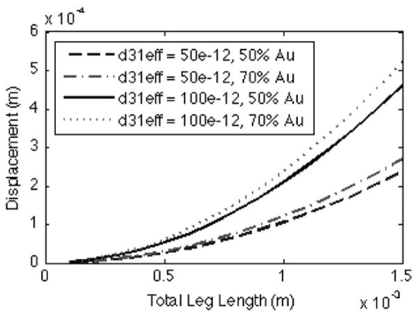
In terms of designs, for a given material stack and voltage, displacement is dependent on the length of the beams used, and the relative length of the bend-up and bend-down (gold-covered) segments. As an illustration of these effects, figure 4 shows displacement versus beam length at 20 V when d31,eff = −50 and −100 pm V−1, and for gold coverage over 50% and 70% of the beam, respectively.
Figure 4.
Sample tip displacements versus beam length and gold coverage at 20 V for nominal material thicknesses and hypothesized effective piezoelectric coefficients of −50 pm N−1 or −100 pm N−1.
3. Fabrication
The translational vertical piezoelectric stages are fabricated by depositing and patterning the piezoelectric material stack and then using deep reactive ion etching (DRIE) and photoresist encapsulation procedures to define the moving structure. This process was performed at the US Army Research Laboratory and based on existing deposition procedures established for piezoelectric microactuator fabrication [20, 25]. A full description of the piezoelectric stack deposition and patterning procedure, including details of PZT chemical-solution-derived deposition and heat treatment, is provided in [25]. In summary, the piezoelectric material stack begins with an elastic layer of silicon dioxide, followed by a sputter-deposited Ti/Pt bottom electrode layer. The PZT thin film is deposited by a chemical-solution process that is a modified version of that by Budd et al [26]. The PZT is then coated with a second Pt electrode. During stack patterning, first the top Pt electrode and then the PZT layer is ion milled using successive lithography masks. A third mask for patterning the PZT stack is used to open wet etch holes in the PZT above the bottom platinum, thus opening up bottom electrodes for wire bonding or other external electrical connections.
A thick gold layer is added to bond pads and bend-up segments of the actuators using a lift-off process. A double exposure technique is used to produce an overhanging photoresist edge profile, improving lift-off reliability for fine features. A titanium/gold bi-layer (20 nm/980 nm) is evaporated via electron beam deposition.
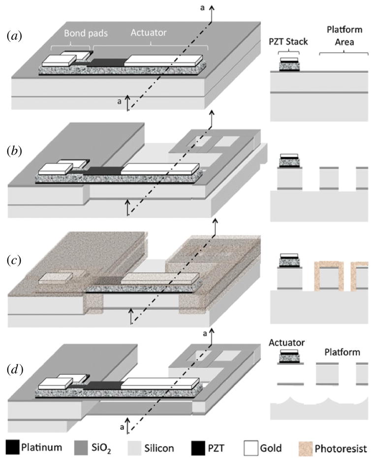
A rendering of the PZT actuator material stack after deposition and patterning, and before bulk processing of the SOI wafer, is shown in figure 5(a). The structural geometry of the actuator and moving platform is then defined lithographically and etched by a combination of DRIE of silicon and reactive-ion etching of silicon dioxide to a depth slightly larger than that of the buried oxide layer, typically 12 μm.
Figure 5.
Vertical stage fabrication process: (a) PZT stack deposition and patterning, (b) actuator and platform definition by deep reactive ion etching, (c) thick photoresist encapsulation of the desired device layer silicon and (d) XeF2 etching and photoresist removal.
To achieve large deflection motion of a comparatively rigid platform, all silicon must be removed from beneath the actuators themselves, but only silicon from the handle wafer should be removed beneath the platform. To accomplish this, a selective photoresist encapsulation is performed, as shown in figure 5(b). The entire surface of the wafer is coated with 9 μm thick photoresist, which is then lithographically patterned to locate etch holes in the bottom surfaces of DRIE trenches surrounding the platform. In addition, the sidewalls of the trenches defining the actuator are exposed, to remove the photoresist coating during development and allow etchants to reach the device layer silicon only in those locations, as shown in figure 5(c).
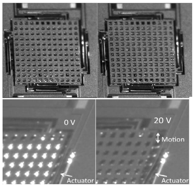
The encapsulated device is released in XeF2, which removes all unencapsulated silicon with an etch depth of approximately 50 μm. The encapsulating photoresist is finally removed in an O2 plasma etch. The resulting actuator-platform structure consists of freely moving actuators attached at one end to the original wafer or die, and at the other end to a rigid silicon platform. Also remaining is a strip of buried oxide directly beneath the actuators, as shown in figure 5(d). Inspection of the actuators via scanning electron microscopy reveals that for actuators of the length utilized for vertical actuation (~1 mm), this buried oxide strip pulls into the piezoelectric stack and adheres to the bottom surface of the original surface oxide. This has been consistent among devices tested to date, and has the effect of stiffening the structure beyond what would be anticipated from the silicon dioxide deposited on the surface of the wafer alone. The additional 0.1 μm buried oxide thickness has been added to the surface oxide thickness of 0.18 μm throughout analytical modeling. In addition, the XeF2 etch does not reach completely to the end of the cantilevers, as designed; finished legs are approximately 80 μm shorter than the prototype design length of 1 mm. An image of a completed vertical actuator is shown in figure 6. Some residual stress is present in the device, resulting in an initial deflection, upon conclusion of processing, of approximately 10 μm in the negative z-direction.
Figure 6.
Top view and oblique view of the corner of a prototype vertical stage under 0 and 20 V.
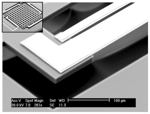
Processing challenges for this device are primarily centered around the XeF2 release process using photoresist encapsulation. A conventional buried oxide etch is not effective for these structures both because of incompatibility between SiO2 etchants, such as hydrofluoric acid, and the PZT film, and because all silicon must be removed underneath the actuator. A sufficiently thick photoresist must be used so as to coat all sidewalls that are to be protected, but not so thick as to prevent full exposure and removal at the bottom of the DRIE trenches. Common flaws observed during fabrication include photoresist encapsulation being too thin over the corners of trenches for adequate protection and insufficient under-etching of released structures by XeF2. Great care must be taken in inspection of the photoresist encapsulation layer before and during XeF2 etching to ensure survival of all desired features. In addition, encapsulation layer release must also be performed using a dry etching process, to avoid damaging the now very thin actuator structures. The structure of the actuator following release is shown in detail in figure 7.
Figure 7.
Scanning-electron microscope image of end of an actuation leg (full actuator inset), showing the XeF2 etching profile below the device layer platform and actuator.
4. Actuator testing
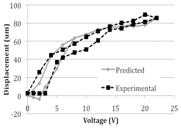
Both static and dynamic vertical actuator deflections were measured experimentally. Static measurements were performed using an optical profilometer to measure the vertical height of the corners of the stage under varying applied voltages. Experimental measurement was begun by poling the PZT thin film at 20 V for 10 min, then stepping back to 0 V in 2 V increments and finally returning to the original deflection by increasing voltage in 2 V increments. While an initial displacement of the stage exceeded 120 μm, the maximum displacement at 20 V following poling was approximately 86 μm.
The experimental results show reasonable agreement with analytical modeling of a stage with 920 μm long legs, given the measurement of d31,eff coefficients from free cantilever test structures on the same wafer and others created by the same fabrication process. Experimental and analytical measurement is particularly good at low and high voltages, as is depicted in figure 8. However, mid-range measurements show greater hysteresis, and smaller deflection than anticipated. While some of this irregularity is due to difficulty in maintaining clear reference points during optical profilometry over the relatively large deflection, it may be that stresses experienced due to un-modeled static loading, possibly the slight torsion effect due to rotation of the stage, complicate stress conditions and increase hysteresis in the beam.
Figure 8.
Experimental measurement of prototype stage displacement versus voltage after device poling at 20 V, compared to displacement.
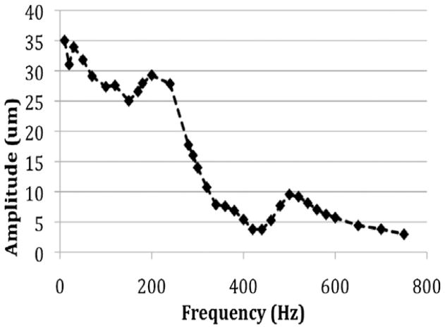
Dynamic testing to identify structural resonance was performed using a laser-Doppler vibrometer (LDV) and examining the response of the system to a swept-sine input. The LDV was focused on the center of the platform, and a sinusoidal input with a nominal voltage of 9 V and a 2 V amplitude was applied to the device. Displacement estimates were integrated from the resulting velocity measurements, shown in figure 10.
Figure 10.
Experimental frequency response to the sinusoidal input with magnitude 2V about 9V dc bias.
The experimental frequency response shows some nonlinearity that would not be predicted from linear actuator moments, or from the estimated platform mass and stiffness of actuated legs. The first apparent resonance occurs at 200 Hz, whereas the natural frequency of the system, given by , would be approximately 300 Hz. If a damping ratio is estimated from the height peak at 200 Hz to be approximately 0.4, the resonant peak would be expected to occur near 240 Hz. In addition, there is an increase in response amplitude at low frequency, inconsistent with a linear mass-spring-damper model. We also observe a second peak at approximately 500 Hz, attributed to the second vibration mode of the beams.
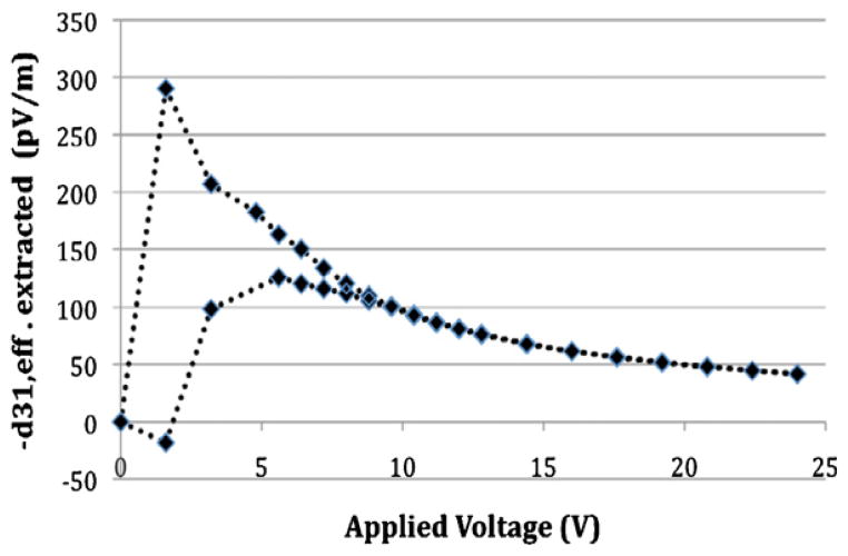
To compare analytical models to experimental measurements, effective piezoelectric coefficients must be known. As mentioned above, d31,eff coefficients for the PZT stack used were estimated by making optical profilometer measurements of free cantilever beams under an applied voltage. A best-fit radius is matched to the deflected beam geometry, which is used to estimate the piezoelectric coefficient using equations (1), (4) and (5). While any error in the elastic moduli used in piezoelectric coefficient calculation will result in an inaccuracy in the exact value for the piezoelectric coefficient, the resulting actuation moment at varying voltages will be consistent across devices using the same layers; this allows the measured nonlinear piezoelectric coefficient to be used in checking analytical models against experimental results. A plot of the estimated d31,eff coefficients is shown in figure 9.
Figure 9.
Extracted effective electro-active –d31,eff estimates versus voltage from simple cantilever beam experiments.
5. Analysis and dynamic modeling
Nonlinear behavior observed during experimental testing of vertical stage frequency response motivates investigation of two possible nonlinear effects on dynamic behavior: (1) beam bending nonlinearity due to large deflection motion, and (2) the nonlinear relationship between effective d31 coefficient and voltage.
When the stage is moving, inertial effects influence the bending profile of the links, leading to a reaction force experienced at the tip of each cantilever. This prevents the use of a closed-form large deflection analysis such as that for predicting static displacements. Over large deflections, a numerical approach is required to most accurately calculate the deflection of the beam, where the primary loads are an internal moment, reaction moment at the tip of each beam and a vertical load force at the tip of the beam. This incorporates the effect of a moment into the large deflection beam analysis method of Belendez et al [27], providing a simple method for numerical analysis when both moment and force are present. A previous study of piezoelectric structures with very similar geometry was performed by Kaya et al but did not incorporate analytical modeling for more general use [28].
5.1. Large deflection analysis
Figure 3 shows a concentrated load force, F, at the free end of the modeled beams, as well as the applied and reaction moments. In this figure Δx and Δz are the horizontal and vertical displacements at the free end, respectively, and θ0 denotes the slope at the end of the beam.
The deflection of the beam satisfies the following equation all the time:
| (12) |
where M(s) is the moment at a specific point along the arc length, s, of the beam
| (13) |
and M0 is the total moment applied through both the actuation moment and the moment at the tip of the beam, ML. The boundary conditions are those of a cantilever beam:
| (14) |
Combining (11) and (12), we have
| (15) |
To convert the right-hand side of (15) into a form that is easily numerically integrated, we note that cos θ. = dx/ds and differentiate, obtaining the differential equation governing the deflections of the beam:
| (16) |
Multiply both sides of this equation by dθ/ds:
| (17) |
which is equivalent to
| (18) |
thus indicating that the quantity inside the parentheses is constant at all times. At the tip of a cantilever beam, dθ is known,
| (19) |
meaning that we can define the contents of (18) according to behavior at the tip, such that
| (20) |
Manipulating (20), and knowing from (18) that the quantity in parentheses is constant for all s, produces the following relationship, which is an equation in the form of Belendez [27] plus an applied moment:
| (21) |
This provides an easily integrable expression for arc length, s,
| (22) |
Using the actual length of a beam in (22) allows one to numerically solve for the tip angle, θ0. Once θ0 is known, the tip deflection may be solved for using the relationship dz/dx = sin θ:
| (23) |
When solving for the displacement of the compound beam used in the z-stage, a further integration process is required. The bending moments on the respective beam segments are given by M0,1 = Mact1 − ML and M0,2 = Mact2 + ML, and each having respective composite moduli. Equation (22) must be iterated as a function of ML to find a solution with equal tip angle on both beam segments, and the resulting ML applied to (23).
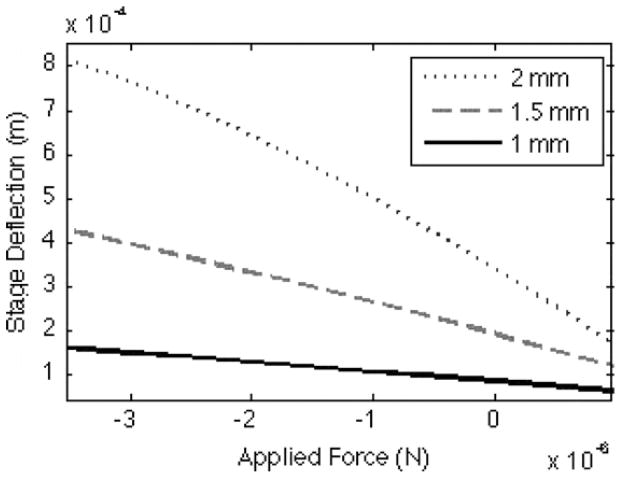
Figure 11 shows the total analytical displacement of beams of varying length with 70% gold coverage for an example input of 20 V with d31,eff = −50 pm V−1. Nonlinear effects prove to be negligible for 1 mm beam lengths, only becoming significant when beam lengths increase to 1.5 mm or 2 mm for large forces in the direction of motion, beyond the range of those likely to be experienced by the stage.
Figure 11.
Vertical deflection versus transverse force for various beam lengths at 20 V.
5.1.1. Effects of nonlinear d31 coefficient
Once it is known that the mechanical stiffness of the stage is subject to linear behavior, the estimated piezoelectric coefficients may be used to better understand nonlinearities in dynamic response to a sinusoidal voltage input, V(t). During simulation, the static displacement of the stage may be calculated using (1), (4), (6) and (7) to provide a nominal displacement as a function of time, znom(V(t)). For stages operating in the linear range with respect to an applied force, the equivalent dynamic force, F(t), on the stage can be calculated by comparing the nominal displacement to the actual current displacement, z(t), by
| (24) |
where k is the equivalent linear spring constant of the beams from (11).
The response of the system to a varying voltage input can then be integrated numerically using the ordinary differential equation
| (25) |
where m is the mass of the actuator platform and b is a damping coefficient. The damping coefficient is estimated from the height of the resonant peak in experimental testing as 74 μN s m−1.
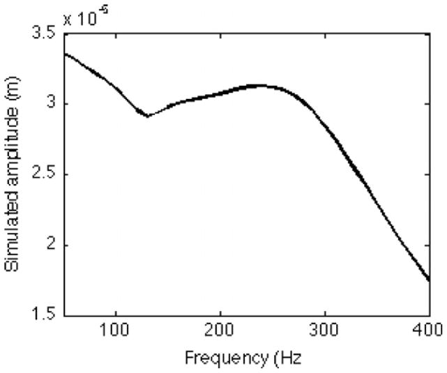
Interpolating from the estimated values of d31,eff for sinusoidal voltage inputs with varying average voltage and magnitude, we observe that the nonlinear piezoelectric coefficient can have a significant effect on the shape of the frequency response. Figure 12 shows the frequency response between the sinusoidal input frequency and the magnitude of an output displacement of a 0.92 mm beam (this length being selected to match that of the fabricated actuators) near the resonant frequency of the system for varying voltage levels. We observe that the simulated frequency response shows a resonance slightly below that which would be predicted from the mass, spring, constant and damping alone (approximately 230 Hz versus 240 Hz), and more prominently, an upward trend in sinusoidal amplitude for low-frequency excitations. While direct use of the estimated piezoelectric coefficients oversimplifies hysteresis behavior, the close agreement between the simulated behavior and experimental results, given processing uncertainty, would strongly indicate nonlinearity as being the primary factor behind unusual behavior of the frequency response.
Figure 12.
Simulated amplitude versus frequency response of a stage using estimated d31,eff coefficients.
6. Discussion
The ability to perform substantial vertical actuation at high speeds with a very thin actuator is potentially useful to a variety of applications. For example, the existing actuator has less than a 3 mm diameter and a total thickness, including handle wafer, of just 550 μm, which is small enough to be used in miniature medical probes for three-dimensional in vivo imaging, especially microendoscope applications [1, 29, 30]. Till now, most existing vertical translational (z-axis) actuators rarely fit microendoscopes, in which the diameter (and length) of each component should be less than 5 mm. To overcome the challenge of miniaturization for future medical devices, the new piezoelectric thin-film-based translational actuator will be incorporated into a prototype fast scanning mechanism. In addition, to take full advantage of deep imaging depth (up to 500 μm) of the target application of dual-axes confocal microscopy, several actuation legs could be placed in series, to extend motion of the stage to a comparable magnitude, at the expense of reduced bandwidth. Multiple legs in series also allow for a folded-leg geometry that eliminates rotary rotion and lateral shifting of the stage (as viewed from above) as the stage moves.
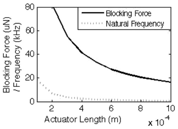
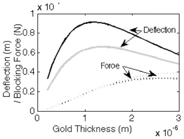
In a more general context, the primary design variables available to the designer are the length of the actuators and the layer thicknesses in the piezoelectric stack. As shown in figure 4, increasing cantilever length leads to a dramatic increase in displacement. As shown in figure 13, this is accompanied by decreasing blocking force of the actuator (approximately equal to the linear spring constant multiplied by displacement and the number of legs) and structural natural frequency. In designing for a specific application, the designer must typically trade-off actuator force or speed for displacement, although large displacements using the thin-film piezoelectric vertical actuator are obtained at higher speeds and with more force than from most vertical microactuators. Variation in performance due to thin-film layer thickness is less dramatic. It is typically possible to obtain a gold thickness optimizing displacement for given silicon dioxide and PZT layer thicknesses, as shown in figure 14. Increasing gold or silicon dioxide thicknesses further tends to reduce displacement, while somewhat increasing blocking force and structural natural frequency.
Figure 13.
Effects of increasing actuation leg length on blocking force and natural frequency, for nominal film thicknesses and 20 V input.
Figure 14.
Deflection and blocking force as a function of gold film thickness at 20 V for actuator with 1 mm long legs and 70% gold thickness, in the cases of 0.25 and 0.5 μm silicon dioxide thicknesses.
For use in optical applications, motion of the stage should be very precise, and will likely ultimately require feedback control strategies. The static and dynamic models described above are important for providing an accurate model of system motion. However, the modeling techniques are subject to certain drawbacks. First, the effective electro-active coefficient of the PZT film must be extracted experimentally, and these experiments rely on reliable knowledge of material properties in the piezoelectric stack. The prototype actuator tested here utilizes an established PZT stack deposition procedure, for which extensive material property testing has previously been performed. It should be noted, as well, that the specific material thicknesses selected were not optimized for vertical stage performance, but rather for operation of other devices on the same silicon wafer, meaning that film thickness optimization could potentially lead to substantial gains in performance.
A second drawback, specific to dynamic simulation, is that the damping coefficient is not easily estimated analytically. To perform dynamic simulations, a linear damping coefficient was estimated from experimental data, based on the peak of the observed apparent resonance and analytically calculated mass and stiffness of the stage. However, we know that behavior near resonance is somewhat distorted by nonlinearity of the piezoelectric coefficient, such that this is unlikely to be the true damping coefficient of the device. Fortunately, the simulation results are relatively insensitive to variation in damping coefficient, such that the procedure above works well for achieving agreement between simulation and experimental models. Still, this does introduce a possibility for bias toward the observed system into the simulation, and makes simulation difficult to perform accurately without experimental measurements to guide damping coefficient selection.
One additional advantage of piezoelectric actuation is low power consumption. The piezoelectric capacitance of the prototype stage at 20 V is approximately 0.7 nF. This corresponds to a power consumption of less than 60 μW at 200 Hz, which is extremely small in comparison to electromagnetic and electrothermal microactuators.
7. Conclusions
A large displacement vertical translational actuator based on piezoelectric thin films is presented. Analytical models of static and dynamic behaviors allow reasonable accuracy in predicting device behavior, provided that certain parameters, namely effective piezoelectric coefficients and approximate damping coefficents, are known. Resulting stages have displayed up to 120 μm displacement, with 80–90 μm displacement being typical. The measured resonant frequency of the actuators was approximately 200 Hz, with dynamic simulations using knowledge of piezoelectric coefficient variation with voltage used to explain unusual frequency response behavior. The large displacement with relatively high resonant frequency should allow use of stages with additional actuation beams placed in series for a variety of optical MEMS applications, including a target application of an endoscope-compatible dual-axes confocal microscope.
Acknowledgments
The authors thank R Piekarz, J Martin, B Power and R Rudy for their help in deposition and patterning of the thin-film PZT material stack at the US Army Research Laboratory.
References
- 1.Liu JTC, Mandella MJ, Ra H, Wong LK, Solgaard O, Kino GS, Piyawattanametha W, Contag CH, Wang TD. Miniature near-infrared dual-axes confocal micro-scope utilizing a two-dimensional microelectromechanical systems scanner. Opt Lett. 2007;32:256–8. doi: 10.1364/ol.32.000256. [DOI] [PMC free article] [PubMed] [Google Scholar]
- 2.Wu L, Xie H. A large vertical displacement electrothermal bimorph microactuator with very small lateral shift. Sensors Actuators A. 2008;145–146:371–9. [Google Scholar]
- 3.Chen SC, Culpepper ML. Design of contoured microscale thermo-mechanical actuators. J Microelectromech Syst. 2006;15:1226–34. [Google Scholar]
- 4.Chu LL, Gianchandani YB. A micromachined 2D positioner with electrothermal actuation and sub-nanometer capacitive sensing. J Micromech Microeng. 2003;13:279–85. [Google Scholar]
- 5.Chen WC, Yeh PI, Hu CF, Fang W. Design and characterization of single-layer step-bridge structure for out-of-plane thermal actuator. J Microelectromech Syst. 2008;17:70–7. [Google Scholar]
- 6.Cho I-J, Yoon E. A low-voltage three-axis electromagnetically actuated micromirror for fine alignment among optical devices. J Micromech Microeng. 2009;19:085007. [Google Scholar]
- 7.Lie C-S, Lin PD. Miniaturized auto-focusing VCM actuator with zero holding current. Opt Express. 2009;17:9754. doi: 10.1364/oe.17.009754. [DOI] [PubMed] [Google Scholar]
- 8.Uchino K. Micro piezoelectric ultrasonic motors. J Electroceram. 2004;13:1385. [Google Scholar]
- 9.Toda R, Yang EH. Normally-latched, large-stroke, inchworm microactuator. J Micromech Microeng. 2007;17:1715–20. [Google Scholar]
- 10.Jeong OK, Konishi S. Fabrication and drive test of pneumatic PDMS micro pump. Sensors Actuators A. 2007;135:849–56. [Google Scholar]
- 11.De Volder M, Peirs J, Reynaerts D, Coosemans J, Puers R, Smal O, Raucent B. Production and characterization of a hydraulic microactuator. J Micromech Microeng. 2005;14:S15–21. [Google Scholar]
- 12.Werber A, Zappe H. Thermo-pneumatically actuated membrane-based micro-mirror devices. J Micromech Microeng. 2006;16:2524–31. [Google Scholar]
- 13.Helmbrecht MA, Srinivasan U, Rembe C, Howe RT, Muller RS. Micromirrors for adaptive-optics arrays. Tech. Digest, 11th IEEE Int. Conf. on Solid-State Sensors, Actuators and Microsystems (Transducers’ 01); Munich, Germany. 2001. pp. 1290–4. [Google Scholar]
- 14.Lee P, McConaghy CF, Sommargren G, Krulevitch P, Campbell EW. Vertical-actuated electrostatic comb drive with in situ capacitive position correction for application in phase shifting diffraction interferometry. J Microelectromech Syst. 2003;11:960–71. [Google Scholar]
- 15.Chung SW, Kim YK. Design and fabrication of 10 × 10 micro-spatial light modulator array for phase and amplitude modulation. Sensors Actuators A. 1999;78:63–70. [Google Scholar]
- 16.Konishi S, Yoshifuji K, Munechika M, Kawaguchi G. Vertical motion microactuator based on the concept of ECLIA (electrostatic controlled linear inchworm actuator). Proc. 15th IEEE Int. Conf. on Micro Electro Mechanical Systems (MEMS’02); Las Vegas, NV, USA. 2002. pp. 602–5. [Google Scholar]
- 17.Kwon S, Milanovic V, Lee LP. Large-displacement vertical microlens scanner with low driving voltage. IEEE Photon Technol Lett. 2002;14:1572–4. [Google Scholar]
- 18.Chiou JC, Kou CF, Lin YJ. A micromirror with large static rotation and vertical actuation. IEEE J Sel Top Quantum Electron. 2007;13:297–303. [Google Scholar]
- 19.Gross SJ, Tadigadapa S, Jackson TN, Trolier-McKinstry S, Zhang QQ. Lead—zirconate–titanate-based piezo-electric micromachined switch. Appl Phys Lett. 2003;83:174–6. [Google Scholar]
- 20.Polcawich RG, Pulskamp SJ, Judy D, Ranade P, Troilier-McKinstry S, Dubey M. Surface micro-machined microelectromechanical ohmic series switch using thin-film piezoelectric actuators. Microw Theory Tech. 2007;55:2642–54. [Google Scholar]
- 21.Hall DA. Nonlinearity in piezoelectric ceramics. J Mater Sci. 2001;36:4575–601. [Google Scholar]
- 22.Muralt P, Kholkin A, Kohli M, Maeder T. Piezoelectric actuation of PZT thin-film diaphragms at static and resonant conditions. Sensors Actuators A. 1996;53:398. [Google Scholar]
- 23.Sharpe WN, Pulskamp J, Gianoia DS, Eberi C, Polcawich RG, Thompson RJ. Strain measurements of silicon dioxide microspecimens by digital image processing. Exp Mech. 2007;46:649–58. [Google Scholar]
- 24.Hemker KJ, Sharpe WN. Microscale characterization of mechanical properties. Annu Rev Mater Res. 2007;47:649–58. [Google Scholar]
- 25.Oldham K, Pulskamp J, Polcawich R, Dubey M. Thin-film PZT lateral actuator with extended stroke. J Microelectromech Syst. 2008;17:890–9. [Google Scholar]
- 26.Budd K, Dey S, Payne S. Sol-gel processing of PbTiO3, PbZrO3, PZT, and PLZT thin films. Proc Br Ceram Soc. 1985;36:107–21. [Google Scholar]
- 27.Belendez T, Neipp C, Belendez A. Large and small deflections of a cantilever beam. Eur J Phys. 2003;23:371–9. [Google Scholar]
- 28.Kaya T, Koser H. A study of nonlinear deflection dynamics of a piezoelectric accelerometer. Proc. COMSOL User’s Conf; Boston, MA. 2005. [Google Scholar]
- 29.Ra H, Piyattanametha W, Mandella MJ, Hsiung P-L, Hardy J, Wang TD, Contag CH, Kino GH, Solgaard O. Three-dimensional in vivo imaging by a handheld dual-axes confocal microscope. Opt Lett. 2007;32:256–8. doi: 10.1364/oe.16.007224. [DOI] [PMC free article] [PubMed] [Google Scholar]
- 30.Wang TD, Mandella MJ, Contag CH, Kino GS. Dual-axis confocal microscope for high-resolution in vivo imaging. Opt Lett. 2003;28:414–6. doi: 10.1364/ol.28.000414. [DOI] [PMC free article] [PubMed] [Google Scholar]


