Abstract
Achieving 180° magnetization reversal with an electric field rather than a current or magnetic field is a fundamental challenge and represents a technological breakthrough towards new memory cell designs. Here we propose a mesoscale morphological engineering approach to accomplishing full 180° magnetization reversals with electric fields by utilizing both the in-plane piezostrains and magnetic shape anisotropy of a multiferroic heterostructure. Using phase-field simulations, we examined a patterned single-domain nanomagnet with four-fold magnetic axis on a ferroelectric layer with electric-field-induced uniaxial strains. We demonstrated that the uniaxial piezostrains, if non-collinear to the magnetic easy axis of the nanomagnet at certain angles, induce two successive, deterministic 90° magnetization rotations, thereby leading to full 180° magnetization reversals.
Electric fields, rather than magnetic fields or current, are required to control magnetic moment directions in order to achieve minimum power consumption in spintronics devices. Multiferroic magneto-electric (ME) materials1,2,3,4,5,6,7,8,9,10,11,12,13,14,15,16,17,18,19,20,21,22,23 are prime candidates for such electric field controlled magnetic switching. However, the application of single-phase multiferroic ME materials is challenged by requirements, such as room temperature operation and strong ME effects. Therefore, multiferroic ME heterostructures comprised of ferromagnetic and ferroelectric layers are increasingly being explored as candidate materials1,2,3. Indeed interesting interfacial coupling mechanisms such as charge/orbital modulation4,5,6, exchange coupling7,8, or/and elastic coupling via strain transfer9,10,11,12,13,14,15,16,17,18,19,20,21,22,23, have been discovered in different multiferroic ME heterostructures. Among them, the elastic coupling mechanism is simple and promising since the strong ME coupling between two ferroic layers at room temperature can be achieved and mediated via the strain transfer across their interfaces. For example, this strain-mediated ME coupling mechanism has been demonstrated to be responsible for modulation of the magnetism by an electric field in a number of ME heterostructures (e.g., see refs. 9–23).
In strain-driven ME heterostructures, of paramount challenge is the reproducible and controllable 180° magnetization reversal with electric fields. Strains only result in at best a rotation of magnetization by 90° in an individual magnetic domain, which is also nondeterministic24. Therefore, in most cases, strain-induced switching is limited to 90° or is assisted by a magnetic field or spin transfer torque5. Alternatively, Iwasaki25 proposed an interesting analytic model to show that the four-fold symmetric magnetocrystalline anisotropy could assist stress-driven magnetization reversal in magnetostrictive films, which required epitaxial or highly textured magnetic films to keep the four-fold symmetric magnetocrystalline anisotropy of magnetostrictive crystals. Recently, Roy et al.26 proposed a binary switching model to reverse the magnetization in an elliptical cylinder shaped Terfenol-D nanomagnet; but a rather higher uniaxial stress is required to drive the magnetization switch out-of-plane at first and then a fast ramp rate is needed to promise the magnetization not to backtrack, in order to accomplish a magnetization reversal. Any step beyond these limitations represents an important breakthrough towards a new memory cell design. In this work, we propose a mesoscale morphological engineering approach to achieving 180° magnetization reversal using electric fields by utilizing magnetic shape anisotropy. As an example, we design a patterned ME heterostructure of a flower-shaped single-domain nanomagnet with four-fold symmetric anisotropy on a ferroelectric layer. Using phase field simulations and thermodynamic analysis, we demonstrate that a 180° magnetization full reversal with pure electric fields can be accomplished by producing two successive, deterministic 90° switches in the patterned single-domain nanomagnet if the easy anisotropy axis of the nanomagnet is non-collinear but cants at an appropriate angle with electric-field-induced magnetoelastic axis. Our finding would provide a simple and novel approach towards 180° magnetization full reversal by electric fields.
Results
Artificial multiferroic ME heterostructure
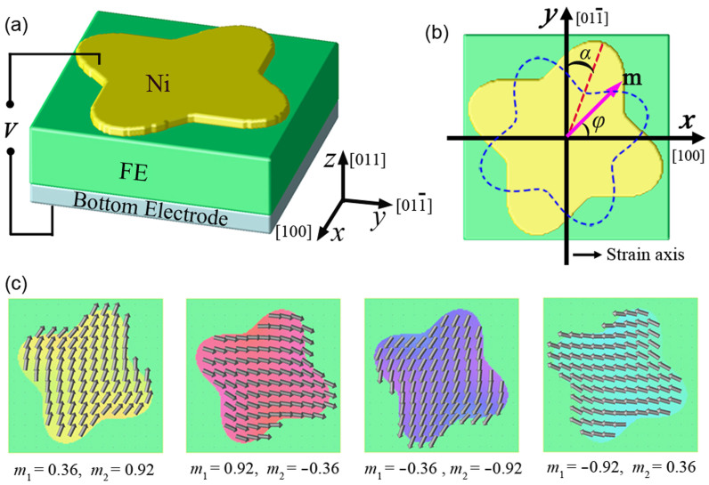
The proposed ferromagnetic nanostructure with a four-fold symmetric shape anisotropy on top of a ferroelectric layer is shown in figure 1a, where the long axis (marked with red dashed line) is tilted at an angle α away from the y direction (see figure 1b). For illustration, the Ni/PMN-PT heterostructure is used as an example. A large anisotropic in-plane piezostrain in the PMN-PT layer produced by an electric field is imparted on its upper Ni layer through interfacial mechanical coupling12,13,14,15,16,17,24,27,28. The phase field method14 (see Method section) is used to model the electric modulation of magnetization in this patterned Ni/PMN-PT heterostructure.
Figure 1. Morphologically engineered artificial multiferroic heterostructure.
(a) Schematic of the heterostructure of a patterned nanomagnet with four-fold shape symmetry grown on a ferroelectric layer (e.g., (011)-PMN-PT). (b) The top view of the Ni nanomagnet on the ferroelectric layer, where y axis denotes the main direction of in-plane anisotropic piezostrain and α the angle between y axis and one of the long axes of the Ni nanomagnet. The blue dashed line represents the shape anisotropy energy contour. (c) Four possible magnetization vector distributions in an as-grown nanomagnet.
The size dependence of magnetic domain structures obtained from the simulations showed that the single-domain state can be stabilized for the patterned artificial Ni nanodot at sizes smaller than 204 nm and 136 nm for the long and short axes. These sizes are large enough for future experimental preparation for validation. The magnetization of the Ni nanodot in the as-grown state can be stabilized along one of the two long axes determined by the four-fold symmetrical shape anisotropy (also termed as configuration anisotropy, see ref. 20). Shown in figure 1c are four equivalent initial states of the magnetization vector distribution in the Ni nanodot, stabilized from a random distribution. Although not entirely uniform, they can be regarded as single-domain states, and the average orientation of the magnetization distribution in these states are along the long axis of the shape anisotropy. Next we take one state with an orientation angle of ϕ = 67° (i.e., with a tilted angle α = 23°; m1 = 0.36 and m2 = 0.92) as an example to demonstrate the magnetization reversal in the Ni nanodot driven by piezostrains via elastic coupling.
Electric field induced 180° magnetization reversal
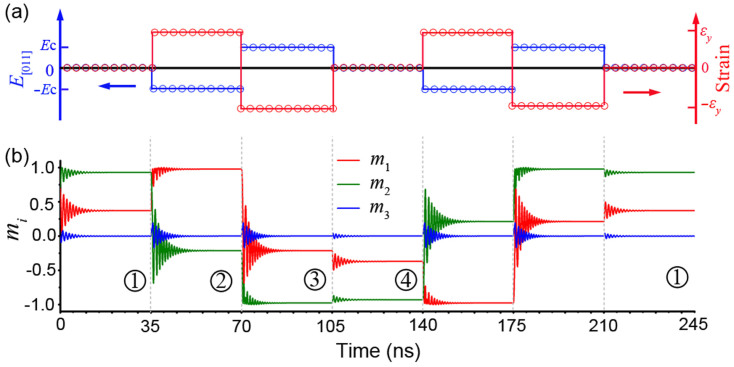
The piezostrains transferred to the Ni nanodot along the y direction (see figure 1b) can be generated by applying an electric field on the engineered (011)PMN-PT layer12,13,14,15,16,17,24,27,28. First, under a negative electric field, which induces a tensile strain εy (see figure 2a) along the y direction, m switches away from the initial state  , precesses, and then shortly (about in 10 ns) stabilizes at state
  with m1 = 0.97 and m2 = −0.21 (figure 2b), i.e., m switches by 79° clockwise. Second, under a positive electric field which induces a compressive strain −εy, m precesses again and stabilizes at state
  with m1 = −0.21 and m2 = −0.97, i.e., m switches by 90° clockwise. After the removal of the electric field, even though the piezostrain is volatile and becomes zero, m relaxes to its nearest shape-anisotropy determined state
  with m1 = −0.36 and m2 = −0.92. Consequently, the magnetization finishes a full 180° reversal through successive switching in the same direction from state
  to state
  . This 180° magnetization full reversal from state
  to state
  driven by a pair of negative and positive electric field pulses is repeatable, i.e., after another pair of negative and positive electric field pulses, m finishes another full 180° reversal from state
  back to state
  , as exhibited from 140 ns to 245 ns in figure 2b. In addition, during each electric-field-induced precession attenuation process, as seen from figure 2b, m3 fluctuates around zero with a small amplitude and stabilizes at zero eventually after a short time, i.e., m lies in the plane of the Ni film.
Figure 2. Electric field induced 180° magnetization reversal.
(a) Electric field pulses (blue) can generate piezostrains (red) along y axis. Here Ec and εy are taken as 0.14 MV/m and 0.07%, respectively (ref. 10). (b) Magnetization switching dynamic behavior driven by electric field pulses. The time scale in (b) indicates the real time of magnetization evolution solved from the LLG equation. At the beginning, the magnetization is evolved from random initial distribution to quasi-stable state at zero electric field.
Discussion
Mechanisms of the electric field induced 180° magnetization reversal
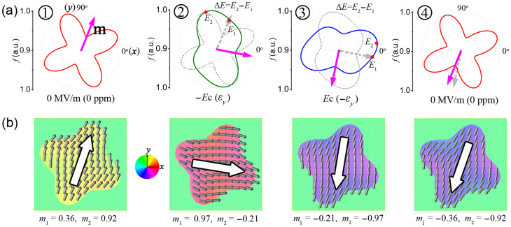
To further understand the piezostrain-driven 180° magnetization reversal, the total free energy F is plotted as a function of the orientation angle of m (see equation 2) assuming uniform magnetization distribution in the Ni nanodot and fully transferred strain from the ferroelectric layer underneath29. For the as-grown Ni nanodot, the energy polar diagram obtained from thermodynamic analysis shows that the magnetization orientation should be along one of the long axes of the shape anisotropy. In the example discussed above, the initial m is assumed to lie in the first quadrant with α = 23°, shown in the energy polar diagram of state  in figure 3a. First, the magnetization is switched away from its initial orientation by the tensile strain on the Ni nanodot along y axis arising from the piezostrain of the (011) PMN-PT layer. The energy polar diagram for the Ni nanodot (see
  in figure 3a) under the tensile piezostrain of εy indicates that m prefers to switch clockwise to the energy minima in the fourth quadrant due to the energy barrier (ΔE = E2 − E1) on the left of the initial m. Similarly, if continuously applying an electric field pulse on the PMN-PT layer to generate a compressive strain on the Ni nanodot, the corresponding energy polar diagram (see
  in figure 3a) indicates that m prefers to continuously switch clockwise away from its previous orientation to finish an almost 180° magnetization reversal. Then, after removal of the electric field, m switches a small angle from state
  to state
  , i.e., to the energy minimum in the third quadrant on the reverse direction of the initial m, finishing a full 180° reversal. The magnetization vector diagrams (see figure 3b) from the phase-field simulations clearly demonstrate the full 180° reversal. Similarly, if the tilted angle α has a negative value (i.e., α = −23°), both the phase field simulations and thermodynamic analysis showed that the magnetization can also accomplish a full 180° reversal by two successive anti-clockwise switching driven by piezostrains. The piezostrain-driven 180° magnetization full reversal is attributed to the synergistic effect of in-plane piezostrain and magnetic shape anisotropy. An important feature of this piezostrain-driven magnetization full reversal is that two magnetic states at 0° and 180° magnetic states (
 and
and  ) are stabilized by the shape anisotropy rather than the piezostrain, thus they would not degrade and be not volatile when piezostrains are completely relaxed.
Figure 3. Mechanisms of the 180° reversal.
(a) Energy polar diagrams of the Ni nanomagnet upon the application of zero electric field (as-grown state), and then successive fields of −Ec, Ec, and zero. Here the gray-dashed and magenta-solid arrows represent the previous and present states of m, respectively, and the energy barrier (ΔE = E2 − E1) ensures the magnetization switch unidirectionally from state  to
to  , and from state
  to
to  . (b) Magnetization vector diagrams corresponding to (a), in which the different background colors represent the orientations of the magnetization as indicated by the color wheel.
Tilting angle of the patterned nanomagnet
For determining the key factors that enable the 180° magnetization full reversal, we calculate the energy barrier ΔE = E2 − E1 (see states  and
and  in figure 3a) which is critical for the unidirectional switching of m. We define a deterministic factor ΔE/kBT (kB being the Boltzmann constant and T the temperature set at 298 K). Similar to the thermal stability factor18,30, a deterministic factor of higher than 40 is required. Figure 4 shows the calculated deterministic factor as a function of the tilted angle α. For the first m-switching from state
  to
to  , figure 4 indicates that the deterministic factor increases with |α| and is larger than 40 when 11° < |α| < 45°. On the other hand, for the switching from state
  to
to  , there is a narrow optimal range of |α|, i.e., 16° < |α| < 37°. Therefore, to ensure the magnetization switching of this Ni nanodot from state
  to
to  through two successive, unidirectional rotations under thermal fluctuation, the tilted angle α should be about 16° < |α| < 37°.
Figure 4. Effect of the tilting angle on the deterministic magnetization switching under electric fields.
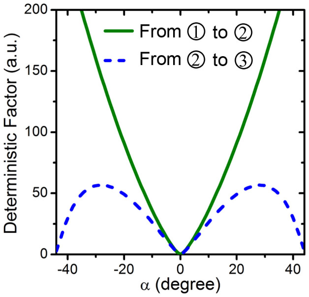
Deterministic factor ( = ΔE/kBT) as a function of the tilting angle α of the patterned nanomagnet.
Strength of the shape anisotropy
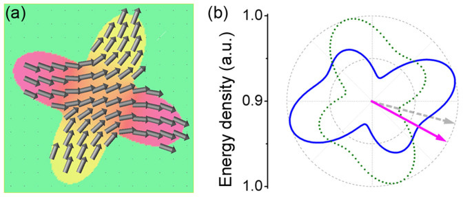
Another key factor that enables the 180° magnetization full reversal is the strength of the in-plane shape anisotropy in the patterned Ni nanodot. Although the shape anisotropy can be enhanced by increasing the difference between its long and short axes, it should not be too large in practical applications. First, a large shape anisotropy (i.e., a large ratio of the long axis to the short axis) results in complex multi-domain structures, as shown in figure 5a. The critical value leading to multi-domain state in this Ni nanodot is about 6.5:3.5. Second, a large shape anisotropy would hinder the unidirectional switching of m. As shown in figure 5b, the energy polar diagrams for the Ni nanodot under tension and compression exhibit four energy minima rather than two, due to the strong four-fold symmetric shape anisotropy. In this case, the magnetization switches by less than 90° clockwise under a compressive strain and switches back counterclockwise under a tensile strain, and thus a magnetization full reversal would not be achieved.
Figure 5. Effect of the shape anisotropy strength on the deterministic magnetization switching under electric fields.
(a) Magnetization vector diagram for the patterned Ni nanomagnet with a larger long axis to short axis ratio of 7:3. (b) Its corresponding energy polar diagrams after applying negative (olive-dashed) and positive (blue-solid) electric field pulses.
In summary, we have demonstrated a simple and new approach towards the nonvolatile 180° magnetization full reversal by an electric field in a multiferroic ME heterostructure via mesoscale engineering of magnetic shape anisotropy. Phase field simulations and thermodynamic analysis clearly demonstrate that the magnetization in a patterned Ni nanomagnet can be switched unidirectionally to complete a 180° magnetization full reversal under pair of tensile and compressive piezostrains transferred from the ferroelectric layers. The electrically driven 180° magnetization full reversal is attributed to the synergistic effect of the in-plane shape anisotropy of the nanomagnet and strain-mediated ME coupling between nanomagnet and ferroelectric layers. Thus, we expect our finding will stimulate future experimental and engineering efforts on developing electric-field controlled devices based on the patterned multiferroic ME heterostructures.
Methods
Phase-field model
In phase field approach, the spatial distribution of the local magnetization m in the Ni nanomagnet is described by the Landau-Lifshitz-Gilbert (LLG) equation, i.e.,
 |
where γ0 and β represent the gyromagnetic ratio and the Gilbert damping constant, respectively, whereby the real time step Δt (~0.17 ps) for the magnetic domain evolution is determined by Δt = Δτ (1 + β2)/(|γ0|MS) with Δτ = 0.02. Heff is the effective magnetic field given by Heff = −(1/μ0)(δF/δM) with μ0 denoting the vacuum permeability and F the total free energy of the nanomagnet,
 |
where fanis, fexch, fms, felastic, and fshape are the magnetocrystalline anisotropy, exchange, magnetostatic, elastic, and shape anisotropy energy densities, respectively. Among them, fanis is neglected for simplicity due to the isotropic nature of the polycrystalline Ni nanomagnet. fexch is determined by the gradient of local magnetization vectors, and fms is obtained using a finite-size-magnet magnetostatic boundary condition14,31,32. The elastic energy density is obtained as before14,31. The thickness of the proposed Ni nanostructure is much smaller than its lateral sizes to permit about 15% strain relaxation33. This consideration allows the mechanical equilibrium equation to be solved using thin-film boundary conditions34 and the relaxed 15% strain decreases the interfacial strain transfer efficiency.
The shape induced anisotropy energy for the nanomagnet is expressed as
 |
where KS is defined as the strength of the in-plane shape anisotropy of the patterned nanomagnet35,36. In the in-plane view of the nanomagnet, the energy contour (the blue dashed curve in figure 1b) due to the shape anisotropy (here the ratio of the long axis to short axis is set as 6:4) indicates the four energy minima corresponding to the two long axes of the shape configuration with KS = 2.9 kJ/m3 (see ref. 37). Note that the shape induced anisotropy field is determined by the size and symmetry of the sample. For instance, for the Ni80Fe14Mo5 nanodot with square shape (150 nm × 150 nm), the shape induced anisotropy field is about 100 Oe37. For Ni nanodot with the same shape and size, this shape anisotropy field corresponds to a value of 2.9 kJ/m3 for KS. The shape anisotropy of the flower-shaped Ni nanodot here should be stronger than that for the square. Experimentally, the shape anisotropy factor KS can be determined by measuring the hysteresis loops when the applied magnetic fields are along the long and short axes, respectively, or can be directly obtained by the so-called modulated field magneto-optical magnetometer technique37.
The temporal evolution of the magnetization vectors is obtained by numerically solving the LLG equation. The material parameters used for simulations, including the saturated magnetization, saturated magnetostrictive coefficients, and elastic constants of Ni layer are the same as used before14, e.g, MS = 4.85 × 10⁵ A/m, λS = −35.0 ppm, c11 = 246.5 GPa, c12 = 147.3 GPa, c44 = (c11 − c12)/2. The discrete grid points of 128Δx × 128Δy × 24Δz with a real grid space Δz = 2 nm, and Δx = Δy = 1.7 nm are employed with the Ni film thickness, hf, of 20 nm. For the patterned Ni nanodot with four-fold in-plane symmetry, the long and short axes are assigned by a ratio of 6:4 using a shape function, i.e.,
 |
Author Contributions
J.J.W. and J.M.H. performed the simulations. C.W.N. and L.Q.C. directed the work. J.J.W., J.M.H., L.Q.C. and C.W.N. co-wrote the paper. J.J.W., J.M.H., J.M., J.X.Z. and C.W.N. analyzed the data. All contributed discussion.
Acknowledgments
This work was supported by the NSF of China (Grant Nos. 51332001, 11234005, 51472140 and 51221291), and the NSF (Grant No: DMR-1410714, DMR-0820404, and DMR-1210588).
References
- Eerenstein W., Mathur N. D. & Scott J. F. Multiferroic and magnetoelectric materials. Nature 442, 759 (2006). [DOI] [PubMed] [Google Scholar]
- Ma J., Hu J. M., Li Z. & Nan C. W. Recent progress in multiferroic magnetoelectric composites: from bulk to thin films. Adv. Mater. 23, 1062 (2011). [DOI] [PubMed] [Google Scholar]
- Vaz C. A. F. Electric field control of magnetism in multiferroic heterostructures. J. Phys: Condens. Matter 24, 333201 (2012). [DOI] [PubMed] [Google Scholar]
- Chun-Gang Duan S. S. & Jaswal E. Y. Tsymbal. Predicted magnetoelectric effect in Fe/BaTiO3 multilayers: ferroelectric control of magnetism. Phys. Rev. Lett. 97, 047201 (2006). [DOI] [PubMed] [Google Scholar]
- Fechner M., Zahn P., Ostanin S., Bibes M. & Mertig I. Switching magnetization by 180° with an electric field. Phys. Rev. Lett. 108, 197206 (2012). [DOI] [PubMed] [Google Scholar]
- Cuellar F. A. et al. Reversible electric-field control of magnetization at oxide interfaces. Nature Commun. 5, 4215 (2014). [DOI] [PubMed] [Google Scholar]
- Chu Y. H. et al. Electric-field control of local ferromagnetism using a magnetoelectric multiferroic. Nature Mater. 7, 478 (2008). [DOI] [PubMed] [Google Scholar]
- Heron J. et al. Electric-field-induced magnetization reversal in a ferromagnet-multiferroic heterostructure. Phys. Rev. Lett. 107, 217202 (2011). [DOI] [PubMed] [Google Scholar]
- Eerenstein W., Wiora M., Prieto J. L., Scott J. F. & Mathur N. D. Giant sharp and persistent converse magnetoelectric effects inmultiferroic epitaxial heterostructures. Nature Mater. 6, 348 (2007). [DOI] [PubMed] [Google Scholar]
- Thiele C., Dorr K., Bilani O., Rodel J. & Schultz L. Influence of strain on the magnetization and magnetoelectric effect in La0.7A0.3MnO3/PMN-PT(001) (A = Sr,Ca). Phys. Rev. B 75, 054408 (2007). [Google Scholar]
- Lou J., Liu M., Reed D., Ren Y. & Sun N. X. Giant electric field tuning of magnetism in novel multiferroic FeGaB/Lead Zinc Niobate–Lead Titanate (PZN-PT) heterostructures. Adv. Mater. 21, 4711 (2009). [Google Scholar]
- Wu T. et al. Electrical control of reversible and permanent magnetization reorientation for magnetoelectric memory devices. Appl. Phys. Lett. 98, 262504 (2011). [Google Scholar]
- Yang L. F. et al. Bipolar loop-like non-volatile strain in the (001)-oriented Pb(Mg1/3Nb2/3)O3-PbTiO3 single crystals. Sci. Rep. 4, 4591 (2014). [DOI] [PMC free article] [PubMed] [Google Scholar]
- Hu J. M., Li Z., Chen L. Q. & Nan C. W. High-density magnetoresistive random access memory operating at ultralow voltage at room temperature. Nature Commun. 2, 553 (2011). [DOI] [PMC free article] [PubMed] [Google Scholar]
- Zhang S. et al. Giant electrical modulation of magnetization in Co40Fe40B20/Pb(Mg1/3Nb2/3)0.7Ti0.3O3(011) heterostructure. Sci. Rep. 4, 3727 (2014). [DOI] [PMC free article] [PubMed] [Google Scholar]
- Liu M. et al. Non-volatile ferroelastic switching of the Verwey transition and resistivity of epitaxial Fe3O4/PMN-PT (011). Sci. Rep. 3, 1876 (2013). [DOI] [PMC free article] [PubMed] [Google Scholar]
- Buzzi M. et al. Single domain spin manipulation by electric fields in strain coupled rrtificial multiferroic nanostructures. Phys. Rev. Lett. 111, 027204 (2013). [DOI] [PubMed] [Google Scholar]
- Franke K. J. A. et al. Size dependence of domain pattern transfer in multiferroic heterostructures. Phys. Rev. Lett. 112, 017201 (2014). [DOI] [PubMed] [Google Scholar]
- Schlom D. G. et al. Elastic strain engineering of ferroic oxides. MRS Bull. 39, 118–130 (2014). [Google Scholar]
- Lahtinen T. H., Franke K. J. & van Dijken S. Electric-field control of magnetic domain wall motion and local magnetization reversal. Sci. Rep. 2, 258 (2012). [DOI] [PMC free article] [PubMed] [Google Scholar]
- Lahtinen T. H., Tuomi J. O. & Dijken S. van Pattern transfer and electric-field-induced magnetic domain formation in multiferroic heterostructures. Adv. Mater. 23, 3187 (2011). [DOI] [PubMed] [Google Scholar]
- Nan T. X. et al. Voltage impulse induced bistable magnetization switching in multiferroic heterostructures. Appl. Phys. Lett. 100, 132409 (2012). [Google Scholar]
- Nan T. X. et al. Quantification of strain and charge co-mediated magnetoelectric coupling on ultra-thin Permalloy/PMN-PT interface. Sci. Rep. 4, 3688 (2014). [DOI] [PMC free article] [PubMed] [Google Scholar]
- Hu J. M. & Nan C. W. Electric-field-induced magnetic easy-axis reorientation in ferromagnetic/ferroelectric layered heterostructures. Phys. Rev. B 80, 224416 (2009). [Google Scholar]
- Iwasaki Y. Stress-driven magnetization reversal in magnetostrictive films with in-plane magnetocrystalline anisotropy. J. Magn. Magn. Mater. 240, 395 (2002). [Google Scholar]
- Roy K., Bandyopadhyay S. & Atulasimha J. Binary switching in a ‘symmetric' potential landscape. Sci. Rep. 3, 3038 (2013). [DOI] [PMC free article] [PubMed] [Google Scholar]
- Hsu C. J., Hockel J. L. & Carman G. P. Magnetoelectric manipulation of domain wall configuration in thin film Ni/[Pb(Mn1/3Nb2/3)O3]0.68-[PbTiO3]0.32 (001) heterostructure. Appl. Phys. Lett. 100, 092902 (2012). [Google Scholar]
- Hu J. M., Li Z., Chen L. Q. & Nan C. W. Design of a voltage-controlled magnetic random access memory based on anisotropic magnetoresistance in a single magnetic layer. Adv. Mater. 24, 2869 (2012). [DOI] [PubMed] [Google Scholar]
- Wang J. J., Hu J.-M., Chen L. Q. & Nan C. W. Strain-domain structure and stability diagrams for single-domain magnetic thin films. Appl. Phys. Lett. 103, 142413 (2013). [Google Scholar]
- Evans R., Chantrell R. W., Nowak U., Lyberatos A. & Richter H.-J. Thermally induced error: Density limit for magnetic data storage. Appl. Phys. Lett. 100, 102402 (2012). [Google Scholar]
- Wang J. J. et al. Effect of strain on voltage-controlled magnetism in BiFeO3-based heterostructures. Sci. Rep. 4, 4553 (2014). [DOI] [PMC free article] [PubMed] [Google Scholar]
- Schabes M. E. & Aharoni A. Magnetostatic interaction fields for a three-dimensional array of ferromagnetic cubes. IEEE Trans. Magn. 23, 3882 (1987). [Google Scholar]
- Nagarajan V. Scaling of the piezoelectric response in ferroelectric nanostructures: An effective clamping stress model. Appl. Phys. Lett. 87, 242905 (2005). [Google Scholar]
- Li Y. L., Hu S. Y., Liu Z. K. & Chen L. Q. Effect of substrate constraint on the stability and evolution of ferroelectric domain structures in thin film. Acta Mater. 50, 395 (2002). [Google Scholar]
- Wadhwa P. & Jalil M. B. A. Micromagnetic modeling and analysis of linear array of square nanomagnets. J. Magn. Magn. Mater. 294, 83 (2005). [Google Scholar]
- Gomonay H. V. & Loktev V. M. Shape-induced phenomena in finite-size antiferromagnets. Phys. Rev. B 75, 174439 (2007). [Google Scholar]
- Cowburn R. P. Property variation with shape in magnetic nanoelements. J. Phys. D: Appl. Phys. 33, R1 (2000). [Google Scholar]


