Abstract
We present a MoS2 biosensor to electrically detect prostate specific antigen (PSA) in a highly sensitive and label-free manner. Unlike previous MoS2-FET-based biosensors, the device configuration of our biosensors does not require a dielectric layer such as HfO2 due to the hydrophobicity of MoS2. Such an oxide-free operation improves sensitivity and simplifies sensor design. For a quantitative and selective detection of PSA antigen, anti-PSA antibody was immobilized on the sensor surface. Then, introduction of PSA antigen, into the anti-PSA immobilized sensor surface resulted in a lable-free immunoassary format. Measured off-state current of the device showed a significant decrease as the applied PSA concentration was increased. The minimum detectable concentration of PSA is 1 pg/mL, which is several orders of magnitude below the clinical cut-off level of ~4 ng/mL. In addition, we also provide a systematic theoretical analysis of the sensor platform – including the charge state of protein at the specific pH level, and self-consistent channel transport. Taken together, the experimental demonstration and the theoretical framework provide a comprehensive description of the performance potential of dielectric-free MoS2-based biosensor technology.
Highly sensitive and rapid detection of biomolecules is essential for biosensors used in clinical, military, or environmental applications. Among various biosensing platforms, biosensors based on field effect transistors (FETs) have been widely investigated to detect a variety of target analytes due to their high sensitivity, label-free detection capability, and compatibility with commercial planar processes for large-scale circuitry1,2,3. Especially, the integration of nanomaterials, such as Si-nanowire (NW), ZnO nanowire, single-walled carbon nanotube (SWNT), or graphene, in a FET configuration offers significant advantages over the label-based techniques for the detection of biological analytes4,5,6. FET biosensors have been demonstrated to be effective in recognizing binding events of charged or polar biological species, because the electrostatic interaction between biomolecules and gate dielectric or channel can give rise to conductance modulation in transistors7.
The biosensors based on one-dimensional (1D) NWs and SWNTs are highly sensitive, but prone to a large deviation of device-to-device performance due to the uncontrolled variations in thickness, purity, chirality, and crystal defects. Additional challenges include the lack of reliable processes of integrating 1D nanomaterials into transistors. On the other hand, the classical Si-FET sensors are easily integrated into massively parallel platform; however, the sensor must be protected from the salt solution by insulators7. As a result, the sensitivity is reduced on two counts: the coupling of the biomolecule to the channel is compromised, the mobility of electrons in the channel is degraded due to surface roughness scattering, and the traps in the oxide increase 1/f noise8,9. Most importantly, the hydrophilic nature of the oxide surface makes surface functionalization difficult and the binding event less efficient.
A new generation of two-dimensional (2D) nanomaterials, such as graphene or transition metal dichalcogenide (TMD), might provide an opportunity for an ultra-sensitive biosensor application because they are compatible with commercial planar processes for the large-scale circuits10,11,12,13. While the zero bandgap of graphene limits the sensitivity of graphene FET-based biosensors, the existence of bandgap in TMDs could enable highly sensitive detection of biomolecular targets by TMD FET-based biosensors14. Interestingly, recent reports exhibit that the surrounding net-charges can easily bring the variation of carrier transport in 2D crystals15,16,17. Such highly sensitive electrical properties of 2D layered semiconductors are attractive for biosensors since the binding event at the interface between MoS2 and charged biomolecules can be monitored by a direct change of the transistor performance metrics including threshold voltage (Vt), field-effect mobility (μeff), and subthreshold swing (SS). The variation of Vt or the conductance for a transistor can be also utilized to measure the number of charged biomolecules onto MoS2 crystals quantitatively. Furthermore, the application of MoS2 FET-based biosensors can become even more promising due to the recent progress in large-area synthesis of 2D MoS2 using chemical vapor deposition (CVD) methods18,19.
Recently, Sarkar et al.14 have reported detection of streptadavin using MoS2 biosensor with HfO2 gate dielectric functionalized with biotin. As discussed previously, many gate dielectrics including HfO2 are hydrophilic and have relatively low affinity to biomolecule adsorption. Therefore, in order to monitor the binding events, the oxide surface needs to be treated with additional chemicals, such as APTES (3-aminoproplytriethoysilane)20. Most of the sensing experiments take place in ionic media. Treatment with chemicals introduces an extra layer of molecules which further increases the separation between the charged biomolecule layer from the sensor surface. This can considerably deteriorate the device sensitivity due to ionic screening21. Recently, Gaur et al.22 have shown that crystalline MoS2 deposited on oxide surface has hydrophobic nature and hence it is expected to have a higher affinity to biomolecule binding. Therefore, MoS2 can serve the dual purpose of surface-adsorption layer as well as sensing layer. This remarkable prospect of oxide-free operation of MoS2 biosensors has not been extensively explored in the literature.
The present work demonstrates the implementation of MoS2 biosensors to electrically detect prostate specific antigen (PSA) in a highly sensitive and label-free manner without the need of a chemically treated gate dielectric. The device configuration of our MoS2 biosensors is utilized as bottom-gated MoS2 FETs with higher sensitivity as well as simpler device structure for oxide-free operation. Here, the nature of hydrophobic MoS2 surface (the contact angle ~75.77°) allows physical adsorption of biomolecules to the sensor surface. Moreover, the use of off-current as an indicator of sensitivity, instead of the subthreshold swing or shift in the threshold voltage, allows additional improvement in device sensitivity in our MoS2 FET biosensors. Theoretical calculation of the MoS2 biosensor operation provides a systematic understanding of the experimental results of the MoS2 biosensors. Theoretical analysis also predicts that controlling defect density and interface trap density is necessary to additionally improve the device sensitivity.
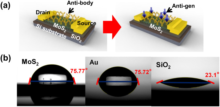
Prostate specific antigen (PSA) has been identified as one of the reliable clinical tools for diagnosing and monitoring prostate cancer. Therefore, the accurate and sensitive detection of PSA at the earliest stage is important for prostate cancer diagnostics and treatment. PSA is typically a negatively charged molecule. To explore the potential for quantitative detection of PSA target with 2D multilayer biosensor, we fabricate bottom-gated MoS2 FETs with higher sensitivity with simpler device structure than those in literature. Fig. 1(a) illustrates the schematic architecture to show label-free immunoassay between an anti-PSA modified MoS2 nanosheet and PSA target in non-aqueous media, unlike the conventional micro-fluidic bio-chip. Anti-PSA (antibody) is physisorbed nonspecifically on the sensing area, and then PSA (antigen) is selectively bound to the immobilized antibody on MoS2 nanosheet, resulting in a classic label-free immunoassay format. It is well known that the proteins retain their ionization state corresponding to the pH of the aqueous solution (PBS) from which they were lyophilized (called “pH memory”)23,24,25. Therefore, the surface charge due to lyophilized proteins results in a stable change in the conductance of the transistor without the need of reference electrode, which is reflected in the drain current as will be discussed later. The first step of fabricating transistors is mechanical exfoliation from bulk MoS2 (SPI Supplies, USA) using scotch tape. Detached thin-film MoS2 flakes are transferred on highly p-doped Si substrate with SiO2 (300 nm). Atomic force microscopy (AFM) measurement shows the thickness of MoS2 flakes in the range of 20–80 nm. Then silicon wafers with SiO2 and MoS2 are cleaned in acetone and IPA for 1 h in order to remove residues. Arrays of 200 × 200 μm2 contacts are patterned by conventional photolithography and lift-off process. Metal contacts of Ti/Au (20 nm/300 nm) are subsequently deposited by e-beam evaporation. To reduce contact resistance, samples are annealed at 200°C with 100 sccm of Ar gas and 10 sccm of H2 gas in a thermal vacuum tube.
Figure 1. A MoS2 nanosheet biosensor and contact angles of different surfaces.
(a) Schematic of a MoS2 biosensor configured as a PSA, detecting label-free immunoassay, illustrating PSA antibody functionalized MoS2 surface (top) and subsequent binding of PSA antigen with antibody receptors. The MoS2 nanosheet biosensor consists of a gate insulator of SiO2 (300 nm) and a drain-source metal contact of Ti/Au (15 nm/300 nm) (b) The water contact angle measurement to confirm hydrophobic characteristics of different substrates: the water contact angle of MoS2, Au, and SiO2 substrate are 75.75°, 75.72°, and 23.1°, respectively. The contact angle of MoS2 surface, which is more hydrophobic than Si-based substrates, is comparable to that of Au surface. This suggests that MoS2 nanosheet is an excellent candidate for functionalizing antibody and protein due to its hydrophobic surface.
As mentioned previously, the hydrophobicity of the MoS2 surface is a key enabling feature, since hydrophobic surfaces have been well known to yield higher affinity of protein-surface adsorption than hydrophilic surfaces. In order to determine degree of hydrophobicity of MoS2, we measure contact angles of MoS2, Au, and SiO2 surface to explore the potential of protein adsorption on MoS2 without a specific surface treatment. In Fig. 1(b), the contact angle of MoS2, Au, and SiO2 are observed as 75.77°, 75.72°, and 23.1°, respectively. While SiO2 surface is hydrophilic with a contact angle of 23.1°, MoS2 and Au surfaces are relatively hydrophobic with contact angles of ~75°. Due to the extremely low contact angles, SiO2 is expected to yield low affinity of protein-surface adsorption, and require an additional treatment of APTES coupled with oxygen plasma-cleaned Si-surface to obtain terminal amine groups26. Since antibody as well as protein is easily immobilized without the complicated surface treatment on Au, the comparable hydrophobicity of MoS2 surface with that of Au surface suggests that MoS2 sensing surface in this study can be functionalized with specific antibody in a non-specific manner.
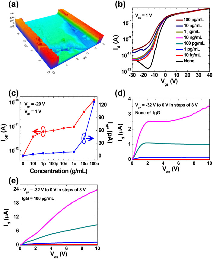
As the first step towards the underlying concept of real-time, electrical direct detection of charged biological species without a specific surface treatment, we investigate the sensor response to adsorption variation on 2D MoS2 crystal as a function of the concentration of charged human Immunoglobulin G (IgG). IgG is the most abundant antibody isotype in human, which has isoelectric point (pI) of ~8.5 (see, Fig. S1 for a theoretical estimate of 8.1). Phosphate buffer solution (PBS, pH = 7.2) is spiked with 7 different concentrations of human IgG that is positively charged at the pH of our measurements. Fig. 2(b) shows the sensor response to the adsorption of 7 different concentrations of human IgG onto MoS2 surface. Characteristics of MoS2 transistors have been shown to be variable with biomolecule adsorption. Here, the on-current (Ion) of the MoS2 transistor shows negligible change with respect to the human IgG concentration, but the off-current (Ioff) of the MoS2 transistor significantly changes with human IgG concentration. We will discuss the theoretical model of the sensor in the next section, but the results are easy to understand intuitively: Without a positively charged human IgG, negative gate voltage during off-state depletes electrons in the n-type MoS2 channel (low off-current, see Fig. 2(b) and Fig. S3). Since human IgG (pI ~ 8.4–8.5) is positively charged at the measurement condition (pH = 7.2), binding of human IgG to the MoS2 surface causes an increase in electrons during off-state. However, during on-state, positive gate voltage accumulates electrons in the n-type MoS2 channel (high on-current) even without human IgG. Hence, the impact of human IgG bound to MoS2 surface on the accumulation of electrons is insignificant. As concentration of human IgG increased from 10 pg/mL to 100 μg/mL, the sensor response (Ioff) also increased (Fig. 2c), indicating that the amount of the adsorbed human IgG on the MoS2 sensor surface is approximately proportional to the applied human IgG concentration. Fig. 2(d) and 2(e) show the output characteristics of the device without IgG and with IgG concentration of 100 μg/mL. Before IgG binding, the sensor shows saturation at high Vds due to channel-pinch off. However, due to positive charge of IgG, the curves become linear reflecting transition from saturation to linear regime. These results provide a potentially important implication that 2D layered MoS2 can be an attractive candidate for a highly sensitive quantitative detection of biomolecular targets without an additional surface treatment.
Figure 2. Adsorption of human IgG onto MoS2 sensor surface.
(a) 3D AFM topography of multi-layer MoS2 with thickness of ~80 nm. (b) Transfer characteristics under various concentration of the human IgG from 0 to 100 μg/mL at Vds = 1 V. (c) Plots of off-current versus human IgG concentration show an increase of off-current with increasing concentration of the human-IgG and abrupt increase of off-current at specific concentration of 10 fg/mL for Vgs = −20 V and Vds = 1 V. Arrows indicate appropriate axis (red: log-scale, blue: linear-scale). (d), (e) Output characteristics under human IgG conditions of 0 and 100 μg/mL from Vgs = −32 V to Vgs = 0 V in steps of 8 V, respectively. Following adsorption of human IgG on MoS2 surface, the drain current exhibits 6-fold increase at a high drain voltage and saturation currents disappear due to the immobile charge of human IgG on the MoS2 nanosheet.
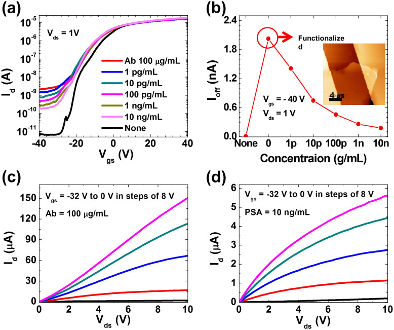
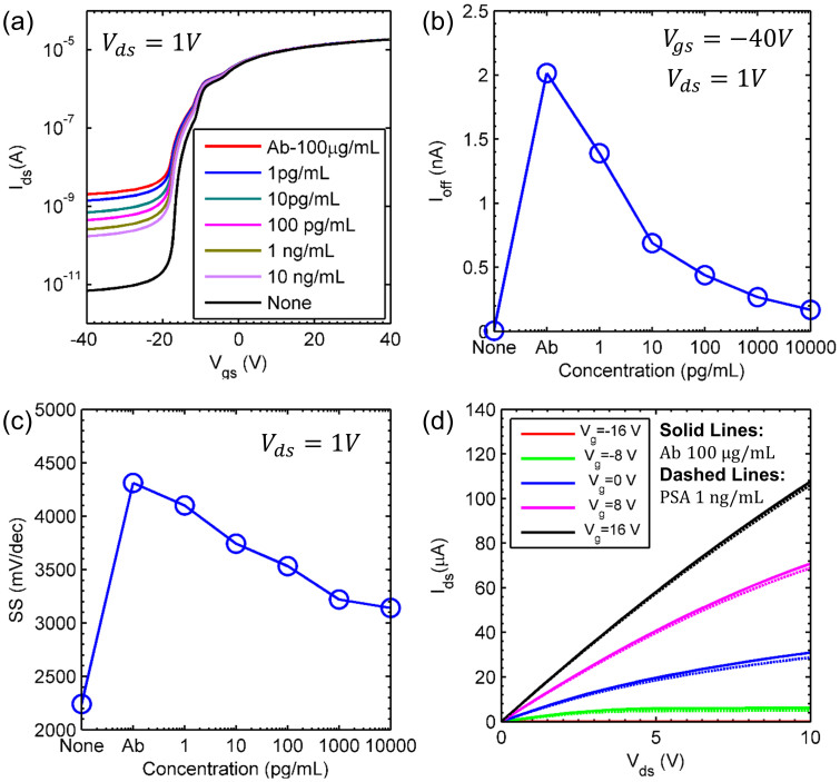
We next investigate the dependence of sensor response on the applied PSA concentration in an anti-PSA functionalized 2D MoS2 nanosheet transistor as shown in Fig. 1(a). Fig. 3(a) shows the increase of off-state current after anti-PSA (antibody) with a concentration of 100 μg/mL is immobilized to the overall MoS2 device surface. The extreme increase of “off-current” in the transistor with anti-PSA physisorbed on the MoS2 nanosheet surface shows a similar trend from adsorption of human IgG onto MoS2 sensor surface, which is consistent with binding of positively charged biomolecules. Then, the off-state current decreases as PSA is selectively bound to the immobilized antibody on the MoS2 surface (Fig. 3(b)). Here, the variation of “off-current” due to the specific binding of negatively charged PSA with the antibodies allows us to monitor highly sensitive detection of PSA markers from 1 pg/mL to 10 ng/mL, and to compute quantitative bioassay from the binding of a charged biological species. As concentration of PSA increased from 1 pg/mL to 10 ng/mL, the increased sensing response with PSA concentration indicates that the amount of the adsorbed PSA on the anti-PSA immobilized MoS2 sensor surface is proportional to the PSA concentration. The minimum detectable concentration of PSA (see, Fig 3(b)) is 1 pg/mL, which is three orders of magnitude below the clinical cut-off level of 4 ng/mL. We will further suggest other approaches to improve sensitivity later in the paper. Fig. 3(c) and (d) shows the output characteristics of the transistor before and after PSA binding. Due to negative charge of PSA, the effective gate voltage on top of MoS2 surface decreases and this leads to current saturation (due to pinch-off) at high drain biases. While the sensor is highly sensitive, the selectivity of the sensor maybe degraded due to physisorption of parasitic molecules on the MoS2layer27. The selectivity of the sensor can however be improved by several methods such as prefilteration steps28, by increasing the incubation time for the adsorption of IgG probe molecules27 or by utilizing the competitive binding of proteins on a hydrophobic surface29,30.
Figure 3. MoS2 nanosheet biosensor for PSA detection.
(a) Transfer characteristics of MoS2 transistor biosensor functionalized by anti-PSA of 100 μg/mL under various PSA concentrations. The surface of MoS2 nanosheet is initially functionalized with anti-PSA antibody receptor. The binding of charged anti-PSA receptors to MoS2 nansosheet gives rise to the off-current increase from 10−12 to 10−9 A of a transistor. (b) Change of the off-current versus various PSA concentrations for an anti-PSA modified n-type MoS2 transistor at the condition of Vgs = −40 V and Vds = 1 V. As the concentration of PSA increases from 1 pg/mL to 10 ng/mL, the amount of selective binding of PSA to the anti-PSA immobilized MoS2 nanosheet is approximately proportional to the PSA concentration. Inset shows an AFM image of MoS2 device with thickness of ~70 nm, width of 12.48 μm and length of 11.64 μm. (c), (d) Output characteristics of MoS2 nanosheet biosensor with functionalized anti-PSA concentration of 100 μg/mL and PSA concentration of 10 ng/mL from Vgs = −32 V to Vgs = 0 V in steps of 8 V, respectively. Current saturation appears and the current decreases by 10-fold due to the charge neutralization associated with the selective reaction between PSA antibody and PSA antigen on the MoS2 nanosheet.
The theory of classical FET-biosensors is well established, but its generalization to double-gated configuration31, especially in the presence of interface defects and pH dependent biomolecule charge require a careful analysis. A semiclassical approach is appropriate because the carrier transport in a sensor is dominated by scattering that can be addressed adequately by a drift-diffusion formulation.
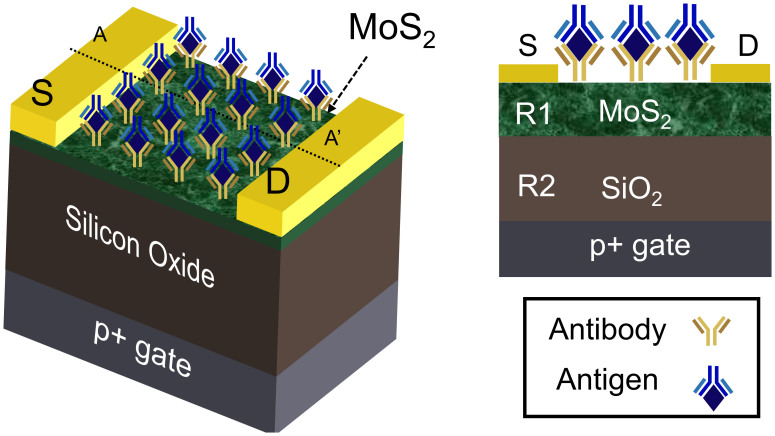
Specifically, in order to interpret the experimental results and to develop a model for MoS2 biosensors, we solved for two-dimensional Poisson and continuity equation self-consistently throughout the device. Table 1 shows the numerical model used for determination of device characteristics (see, Fig. 4). Here, ϕ is the electrostatic potential, n and p are electron and hole concentrations in MoS2 layer, respectively; the channel is presumed n-doped with intrinsic doping density Nd ~ 1 × 1016 cm−3, and μ and D are mobility and diffusion coefficients, respectively. For simplicity, the biomolecule charge is considered as a uniform surface charge sheet with density (σbio) at the top MoS2 surface. This charge is obtained by calibrating the off-current values from the experiment with the simulation, see Fig. S2 (a). The response due to the biomolecules is compromised by the interface traps at top MoS2 surface (σit,top) and MoS2/oxide interface(σit,bottom). The parameters for protein charge and the device parameters are summarized in Supplementary Tables S3–S4, and the list of the symbols is described in Supplementary Table S5 and Supplementary Table S6.
Table 1. Numerical equations for MoS2 sensor.
| Regions 1 & 2 (R1 and R2) | −∇.(ε∇ϕ) = q(p – n +  ) ) |
| Region 1 (R1) | ∇.(qDn∇n – qμnn∇ϕ) = 0 |
| ∇.(−qDp∇p – qμpp∇ϕ) = 0 | |
| Source contact | ϕ = 0 |
| Drain contact | ϕ = Vds |
| Gate contact | ϕ = Vgs – ϕms |
| where | |
 |
|
| MoS2 – SiO2 interface |  |
| Top MoS2 surface |  |
Figure 4. Schematic of the device used for numerical simulation of device characteristics.
Fig. 5(a) shows the transfer characteristics of the device (as a function of backgate voltage) for different PSA concentrations. The simulation results explain consistently the three key features observed in the experiments (refer, Fig. 3) i.e., a) Saturation of current at large negative biases, b) the decrease in subthreshold-swing, and c) the decrease in on-current with the increase (not shown) in PSA concentration. The off-current results from the formation of a conduction channel (accumulated electrons) at the top MoS2 surface in response to the positive charge (at pH = 7.78) of the anti-PSA (antibody) at the top MoS2 surface. For the energy band-diagram along the channel, see. Fig. S3. The negatively charged PSA neutralizes some of the positive charge, and hence off-current decreases with increase in PSA concentration, see Fig. 5(b).
Figure 5. Simulated MoS2 device characteristics for PSA detection.
(a) Transfer characteristics at Vds = 1 V; (b) Off-current at Vds = 1 V and Vgs = −40 V as a function of PSA concentration; (c) Average Subthreshold swing (between −10 V and −20 V) as a function of the PSA concentrations; and (d) Output characteristics of MoS2 sensor with and without PSA on a surface, which has been pre-functionalized with anti-PSA.On-current decreases due to negative charge of PSA.
Similarly, the average subthreshold-swing (SS) of the device increases upon addition of positively charged anti-PSA due to increase in off-current. However, as the concentration of the negatively charged PSA is increased from 1 pg/mL to 10 ng/ml, the off-current decreases tenfold from ~2 nA to 0.2 nA (Fig. 5b vs. Fig. 3b), hence the average subthreshold slope reduces from 4.3 V/dec to 3.1 V/dec as shown in Fig. 5(c). Fig. 5(d) shows the Ids-Vds characteristics for the device with anti-PSA, and with 1 ng/mL PSA concentration. The on-current of the device reduces as PSA is added to the solution, consistent with observations in Fig. 3.
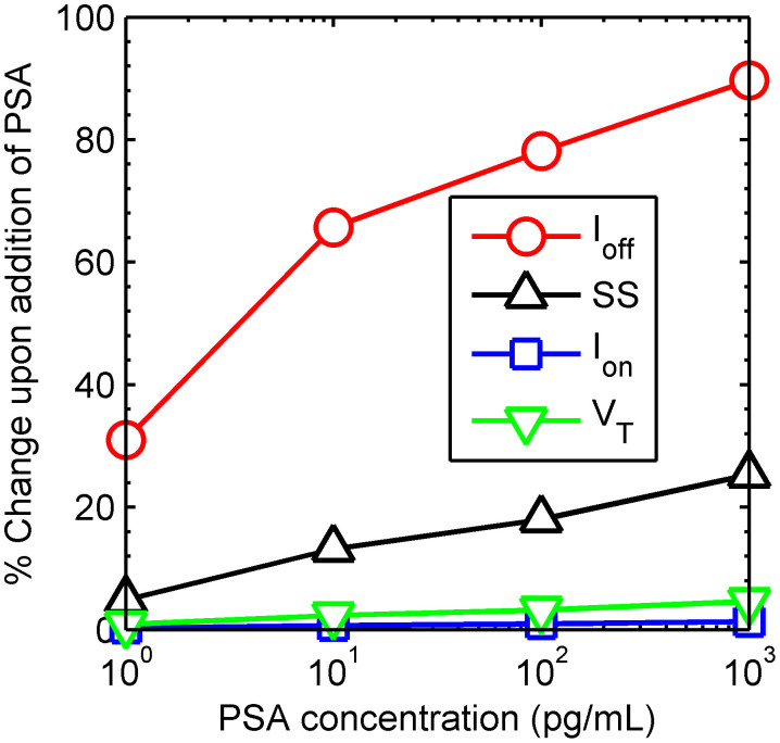
Fig. 6 shows the comparison of sensitivity based on 4 different device parameters, i.e., off-current, Ioff (at Vgs = −40 V), average subthreshold-swing, SS (between −20 V and −10 V), linear threshold-voltage, VT and on-current, Ion (Vgs = 16 V, Vds = 10 V). And the figure explains why the off-current – more so than any other metric – is such a robust indicator of the capture of biomolecules.
Figure 6. Comparison of sensitivity based on 4 different device parameters.
The base value used is for a MoS2 surface with anti-PSA bound on its surface. The off-current shows a considerably larger change upon PSA binding as compared to the subthreshold-swing, threshold voltage and on-current.
Since the MoS2 sensor is accumulation mode device, the relative change in on-current of the transistor is very small. This is because the channel is highly conducting when the device is turned on and a small change in surface charge due to PSA binding causes a corresponding small change in the drain current. However, when the device is completely off, the channel is off and a small change in surface charge due to PSA binding brings relatively larger change in drain current. Unlike Lee7, the capture of PSA does not passivate/create any interface defects, therefore the very small change in VT and SS reflect, only as a secondary metric, the changes in the off current.
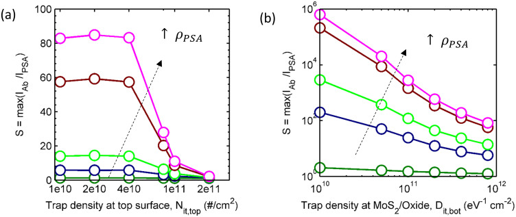
The theoretical interpretation of the experimental results suggests opportunity for future optimization. The relatively large subthreshold slope of the MoS2 discussed in this paper (~2.2 V/dec before and ~4.3 V/dec after anti-PSA decorates the surface) reflects relatively high density of interface traps at the top MoS2 surface and MoS2/oxide interfaces. Fig. 7 suggests that the performance of MoS2 biosensor would improve approximately 40 times for PPSA = 10 ng/mL, if surface treatment could reduce the defect density at the top MoS2 surface by a factor of 5, i.e., from 2 × 10¹¹ # cm−2 to 4 × 10¹⁰ # cm−2. The reduction of defect density at the MoS2/oxide interface has even more dramatic consequences: Sensitivity at the same concentration (ρ = 10 ng/mL) improves by almost 4 orders of magnitude as the trap density is reduced from 8 × 10¹¹ eV−1cm−2 to 1 × 10¹⁰ eV−1cm−2. Therefore, while the experimental results already demonstrate considerable potential of MoS2 based technology in terms of sensitivity, selectivity, fluid stability, and integration on Si-substrate, significant additional improvements are expected with improvement in surface treatment and interface passivation.
Figure 7. Improving the sensitivity by interface passivation.
(a) Variation of MoS2 sensitivity as a function of interface trap densities at top surface of MoS2 for different PSA concentrations (with Dit,bot = 8 × 10¹¹ eV−1cm−2)) b) Variation of MoS2 sensitivity as a function of interface trap density at MoS2-oxide interface (with Nit,top = 4 × 10¹⁰ eV−1cm−2) for different PSA concentrations: 1 pg/mL (Green), 10 pg/mL (Blue), 100 pg/mL (Lime), 1 ng/mL (Brown), 10 ng/mL (Magenta).
In summary, we report a comprehensive investigation on the highly sensitive biosensor platform based on multilayer MoS2 FETs to detect PSA. Our results demonstrate the successful use of MoS2 FET sensor in back-gated scheme without the need of the insulating oxide on the top of channel. The highly hydrophobic nature of the MoS2 surface allows it to serve the dual roles of the transducer and the recognition layer, with considerable improvement in sensitivity and significant simplification of device design. The absence of the oxide layer avoids the additional complexity involved in chemical treatment of the surface, and hence ensures effective coupling of biomolecule charge to the channel. Our theoretical model explains the experimental results consistently and indicates that the sensitivity can be further improved through surface treatment and interface passivation. Combined with the rapid advances in large-area synthesis methods of MoS2 such as CVD, these results deliver a compelling case of potentially using multilayer MoS2 FETs as biosensors.
Author Contributions
J.L. and S.K. designed the experiments. Y.L. and W.C. fabricated the devices, and Y.L., H.P. and W.C. characterized the sensors. P.D. and M.A.A. planned the theoretical analysis; P.D. did the numerical simulation. J.L., S.K., M.A.A. and P.D. wrote the manuscript. All authors reviewed the manuscript. J.L., P.D. and Y.L. contributed equally to this work.
Supplementary Material
Supplementary Information
Acknowledgments
This research was also supported by the National Research Foundation of Korea (NRF-2013M3C1A3059590, NRF-2012R1A1A1042630) and through the NCN-NEEDs program, which is funded by the National Science Foundation, contract 1227020-ECE, and by the Semiconductor Research Corporation.
References
- Makowski M. S. & Ivanisevic A. Molecular analysis of blood with micro-/nanoscale field-effect-transistor biosensors. Small 7, 1863–75; 10.1002/smll.201100211 (2011). [DOI] [PMC free article] [PubMed] [Google Scholar]
- Sarkar D. & Banerjee K. Proposal for tunnel-field-effect-transistor as ultra-sensitive and label-free biosensors. Appl. Phys. Lett. 100, 143108; 10.1063/1.3698093 (2012). [DOI] [Google Scholar]
- Stern E. et al. Label-free immunodetection with CMOS-compatible semiconducting nanowires. Nature 445, 519–22; 10.1038/nature05498 (2007). [DOI] [PubMed] [Google Scholar]
- Cui Y., Wei Q., Park H. & Lieber C. M. Nanowire nanosensors for highly sensitive and selective detection of biological and chemical species. Science 293, 1289–92; 10.1126/science.1062711 (2001). [DOI] [PubMed] [Google Scholar]
- Maehashi K. et al. Label-free protein biosensor based on aptamer-modified carbon nanotube field-effect transistors. Anal. Chem. 79, 782–7; 10.1021/ac060830g (2007). [DOI] [PubMed] [Google Scholar]
- Ohno Y., Maehashi K. & Matsumoto K. Label-free biosensors based on aptamer-modified graphene field-effect transistors. J. Am. Chem. Soc. 132, 18012–3; 10.1021/ja108127r (2010). [DOI] [PubMed] [Google Scholar]
- Lee K., Nair P. R., Scott A., Alam M. a. & Janes D. B. Device considerations for development of conductance-based biosensors. J. Appl. Phys. 105, 102046; 10.1063/1.3116630 (2009). [DOI] [PMC free article] [PubMed] [Google Scholar]
- Deen M. J., Shinwari M. W., Ranuárez J. C. & Landheer D. Noise considerations in field-effect biosensors. J. Appl. Phys. 100, 074703; 10.1063/1.2355542 (2006). [DOI] [Google Scholar]
- Go J., Nair P. R. & Alam M. a. Theory of signal and noise in double-gated nanoscale electronic pH sensors. J. Appl. Phys. 112, 34516; 10.1063/1.4737604 (2012). [DOI] [PMC free article] [PubMed] [Google Scholar]
- Geim A. K. & Novoselov K. S. The rise of graphene. Nat. Mater. 6, 183–91; 10.1038/nmat1849 (2007). [DOI] [PubMed] [Google Scholar]
- Lin Y.-M. et al. Wafer-scale graphene integrated circuit. Science 332, 1294–7; 10.1126/science.1204428 (2011). [DOI] [PubMed] [Google Scholar]
- Wang H. et al. Integrated circuits based on bilayer MoS2 transistors. Nano Lett. 12, 4674–80; 10.1021/nl302015v (2012). [DOI] [PubMed] [Google Scholar]
- Radisavljevic B., Radenovic a., Brivio J., Giacometti V. & Kis a. Single-layer MoS2 transistors. Nat. Nanotechnol. 6, 147–50; 10.1038/nnano.2010.279 (2011). [DOI] [PubMed] [Google Scholar]
- Sarkar D. et al. MoS2 field-effect transistor for next-generation label-free biosensors. ACS Nano 8, 3992–4003; 10.1021/nn5009148 (2014). [DOI] [PubMed] [Google Scholar]
- Zhu C. et al. Single-layer MoS2-based nanoprobes for homogeneous detection of biomolecules. J. Am. Chem. Soc. 135, 5998–6001; 10.1021/ja4019572 (2013). [DOI] [PubMed] [Google Scholar]
- Perkins F. K. et al. Chemical vapor sensing with monolayer MoS2. Nano Lett. 13, 668–73; 10.1021/nl3043079 (2013). [DOI] [PubMed] [Google Scholar]
- Choi W. et al. High-detectivity multilayer MoS(2) phototransistors with spectral response from ultraviolet to infrared. Adv. Mater. 24, 5832–6; 10.1002/adma.201201909 (2012). [DOI] [PubMed] [Google Scholar]
- Liu K.-K. et al. Growth of large-area and highly crystalline MoS2 thin layers on insulating substrates. Nano Lett. 12, 1538–44; 10.1021/nl2043612 (2012). [DOI] [PubMed] [Google Scholar]
- Zhan Y., Liu Z., Najmaei S., Ajayan P. M. & Lou J. Large-area vapor-phase growth and characterization of MoS(2) atomic layers on a SiO(2) substrate. Small 8, 966–71; 10.1002/smll.201102654 (2012). [DOI] [PubMed] [Google Scholar]
- Wang L. et al. Functionalized MoS(2) nanosheet-based field-effect biosensor for label-free sensitive detection of cancer marker proteins in solution. Small 10, 1101–5; 10.1002/smll.201302081 (2014). [DOI] [PubMed] [Google Scholar]
- Nair P. R. & Alam M. a. Screening-limited response of nanobiosensors. Nano Lett. 8, 1281–5; 10.1021/nl072593i (2008). [DOI] [PubMed] [Google Scholar]
- Gaur A. P. S. et al. Surface energy engineering for tunable wettability through controlled synthesis of MoS2. Nano Lett. 14, 4314–21; 10.1021/nl501106v (2014). [DOI] [PubMed] [Google Scholar]
- Meyers R. A. Molecular Biology And Biotechnology. (New York: Wiley, 1995). [Google Scholar]
- Costantino H. R., Griebenow K., Langer R. & Klibanov A. M. On the pH memory of lyophilized compounds containing protein functional groups. Biotechnol. Bioeng. 53, 345–348; 10.1002/(SICI)1097-0290(19970205)53:3<345::AID-BIT14>3.0.CO;2-J (1997). [DOI] [PubMed] [Google Scholar]
- Zaks A. & Klibanov A. M. Enzyme-catalyzed processes in organic solvents. Proc. Natl. Acad. Sci. 82, 3192–3196; 10.1073/pnas.82.10.3192 (1985). [DOI] [PMC free article] [PubMed] [Google Scholar]
- Wang Z.-H. & Jin G. Covalent immobilization of proteins for the biosensor based on imaging ellipsometry. J. Immunol. Methods 285, 237–43; 10.1016/j.jim.2003.12.002 (2004). [DOI] [PubMed] [Google Scholar]
- Nair P. R. & Alam M. a. Theory of “Selectivity” of label-free nanobiosensors: A geometro-physical perspective. J. Appl. Phys. 107, 64701; 10.1063/1.3310531 (2010). [DOI] [PMC free article] [PubMed] [Google Scholar]
- Stern E. et al. Label-free biomarker detection from whole blood. Nat. Nanotechnol. 5, 138–42; 10.1038/nnano.2009.353 (2010). [DOI] [PMC free article] [PubMed] [Google Scholar]
- Choi S. & Chae J. A Physisorbed Interface Design of Biomolecules for Selective and Sensitive Protein Detection. J. Assoc. Lab. Autom. 15, 172–178; 10.1016/j.jala.2009.09.002 (2010). [DOI] [Google Scholar]
- Choi S., Wang R., Lajevardi-Khosh A. & Chae J. Using competitive protein adsorption to measure fibrinogen in undiluted human serum. Appl. Phys. Lett. 97, 253701; 10.1063/1.3529445 (2010). [DOI] [Google Scholar]
- Ahn J.-H. et al. Double-gate nanowire field effect transistor for a biosensor. Nano Lett. 10, 2934–8; 10.1021/nl1010965 (2010). [DOI] [PubMed] [Google Scholar]
Associated Data
This section collects any data citations, data availability statements, or supplementary materials included in this article.
Supplementary Materials
Supplementary Information


