Abstract
Solid-state photomultipliers (SSPMs) are a compact, lightweight, potentially low-cost alternative to a photomultiplier tube for a variety of scintillation detector applications, including digital-dosimeter and medical-imaging applications. Manufacturing SSPMs with a commercial CMOS process provides the ability for rapid prototyping, and facilitates production to reduce the cost. RMD designs CMOS SSPM devices that are fabricated by commercial foundries. This work describes the characterization and performance of these devices for scintillation detector applications.
This work also describes the terms contributing to device noise in terms of the excess noise of the SSPM, the binomial statistics governing the number of pixels triggered by a scintillation event, and the background, or thermal, count rate. The fluctuations associated with these terms limit the resolution of the signal pulse amplitude. We explore the use of pixel-level signal conditioning, and characterize the performance of a prototype SSPM device that preserves the digital nature of the signal. In addition, we explore designs of position-sensitive SSPM detectors for medical imaging applications, and characterize their performance.
Keywords: Solid-state Photomultiplier, CMOS, Photodetector, Scintillation detector, GPD, APD
1. Introduction
Advances in scintillation detectors, including the development of high-performance materials, such as LaBr (Ce) and CeBr [1, 2], and neutron selective materials, such as CLYC [3], stimulates the serendipitous development of improved optical detectors for these new scintillation materials. Photomultiplier tubes (PMTs) are traditionally used for detecting small scintillation pulses, however, advances in detectors are sought to reduce power, size and cost. The recent development of solid-state photomultipier detectors, or silicon photomultiplier detectors, represents a promising candidate detector technology to augment the use of PMTs in certain applications.
SSPMs are arrays of Geiger photodiode (GPD) elements that are read-out in parallel. Figure 1 illustrates the operating principle associated with the use of an SSPM detector with a scintillation detector, where the amplitude of the optical scintillation pulse is proportional to the number of GPD elements that are triggered by its detection.
Figure 1.

Concept of the solid-state scintillation detector, where the scintillation material converts the detection of a gamma-ray or neutron event into an optical pulse. The optical pulse is detected by a solid-state photomultiplier. The number of GPD elements that are triggered by the optical pulse is proportional to the amplitude of the optical pulse.
The GPD elements are essentially small avalanche photodiode pixels operated above the reverse-bias breakdown voltage [4–6], referred to as Geiger-mode operation. For repeated detection, the GPD pixels must be quenched, which can be accomplished by introducing a resistor in series, analogous to the ballast resistor in a Geiger tube, with each pixel.
The fabrication of GPD arrays with integrated resistors [7] provides the basis for the SiPM, or SSPM, device, where the number of pixels triggered correlates to the amplitude of the scintillation pulse. This approach provides a sensitive solid-state optical detector for scintillation detector applications. The use of commercially available CMOS processes to fabricate SSPM devices [8, 9] facilitates the integration of components, including the quenching resistor, with the GPD element.
This work presents SSPM characteristics important for gamma-ray scintillation applications, including the calibration of the energy spectra and the simulation of the expected energy resolution for SSPM detectors, as a function of the number of GPD elements and the excess bias. This work also describes the integration of selected components into the CMOS SSPM device for scintillation detection applications and discusses their merits and drawbacks. The selected integrated components include pixel-level signal conditioning, which preserves the digitization of the signal by the GPD elements, and interconnecting resistor networks to provide a position-sensitive readout for imaging applications, such as PET.
2. Methods and Experiments
2.1. Calibration of gamma-ray spectra
In gamma-ray spectroscopy applications, the pulse-height histograms from the detector must be converted from ADC channels in the gamma-ray energy. The finite number of elements in the SSPM device produces a saturation curve in the number of triggered pixels as a function of increasing light-pulse amplitude, or increasing gamma-ray energy. To convert the ADC channel, i, from the MCA, which is proportional to the number of triggered pixels, to gamma ray energy, E, we use a two-point calibration. The fit of the calibration data to Equation (1) [10], below, recovers the constants A, and k,
| (1) |
where A is the conversion factor, which is generally proportional to the effective number of pixels in the SSPM, and k is the saturation constant, which is related to the fraction of pixels triggered by an event with an energy E.
After converting the x-scale from MCA bins to the energy of the detected gamma ray, the intensities must be “renormalized” to conserve the number of events in the spectrum. The intensity of the MCA data in each channel, Ii, is adjusted using Equation (2) to conserve the number of events in the spectrum.
| (2) |
To demonstrate the correction of the non-linear SSPM response in the energy spectra, gamma-ray spectra were measured with a 1.5mm × 1.5mm SSPM with a 61% fill factor, from the chip referred to as the AE217. The SSPM is composed of 21×21 GPD pixels with active dimensions of 50μm × 50μm. The SSPM was connected to standard nuclear detector electronics.
A 1.5mm×1.5mm×3mm LYSO scintillation crystal, which is coupled to the SSPM with optical grease, converts the gamma-ray events from a 22Na source into optical pulses. The shaping time was 250 ns, which is longer than the width of the GPD pulse, ~50 ns. The time constant associated with the scintillation event is on the order of 60 ns [11].
2.2. Energy resolution simulations
In scintillation detection applications, the noise terms are often described with respect to the pulse amplitude resolution, or gamma-ray energy resolution. Previous work [10] describes the relation between the relative fluctuations, σn/n, in the number of triggered pixels, referred to as the pixel multiplicity, and SSPM device characteristics. Equation (3) relates the expression for the relative energy resolution, (σE/E)det, in terms of the expression for the fluctuations in the pixel multiplicity.
| (3) |
This results in the following expression for the energy resolution of the SSPM detector in terms of the SSPM characteristics.
| (4) |
where FSSPM is the excess noise factor of the SSPM, 〈nt〉 is the average number of pixels trigged by the scintillation event, nttl is the total number of GPD elements (pixels) in the array, and 〈ndark〉 is the average number of dark events from the SSPM within the time profile of the GPD pulse, which is ~50ns for our GPD pixels. In this expression, there is no explicit shaping time and the results are only valid for fast scintillation pulses, i.e., scintillation pulses that are fast relative to the time profile of the GPD pulse.
This expression enables us to examine the dependence of the expected energy resolution performance on SSPM design and operating characteristics, such as the number of pixels in the device and the excess bias.
Simulations using Equation (4) were performed using “typical” SSPM characteristics, from the AE217 chip, and extreme cases to illustrate the effect of various parameters, such as the dark counts and excess noise, on the energy resolution. The dark counts are calculated by multiplying the dark count rate (DCR) times the time associated with the GPD pulse. The excess noise refers to the degradation of the energy resolution performance by cross talk. In the simulations, the amplitude of the optical pulse was assumed to be ~15,000 photons, which is typical for a 511-keV event from LYSO scintillation crystal.
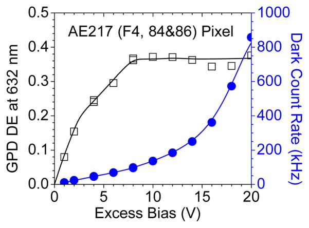
The simulation of the energy resolution dependence on the excess bias uses data based on experimental measurements. Figure 2 shows the data used for simulating the excess bias dependence of the energy resolution for SSPM devices with the following three sizes, in terms of the total number of pixels in the device: 300, 700, and 7000.
Figure 2.
Plot of the excess bias dependence for the detection efficiency, DE and the dark count rate (DCR) for a single GPD pixel. The DCR include contributions from after pulsing.
The DE dependence at 632-nm is used in our simulations. Although other wavelengths may be more appropriate for different applications, such as 420 nm for PET, the overall trends will be similar to those seen with the 632-nm DE data.
The DCR for the GPD pixel illustrated in the figure is one of the highest that we have measured compared to other test pixels. We use this “worst case” data because the effect of the dark noise on the energy resolution of a 511-keV is expected to be small.
The dependence of the DCR on the excess bias, illustrated in Figure 2 includes contributions from after pulsing, which effectively increases the noise from the DCR background. In the energy resolution simulation, we assume this increase in after pulsing does not affect the excess noise of the device, FSSPM, because any signal integration is equal to or less than the time of the Geiger pulse. In the simulation, the magnitude of the DCR background increases with the number of GPD elements in the SSPM detector, i.e., the SSPM area is not held constant as the number of GPD elements is increased.
The excess bias dependence of the excess noise is approximated with the following empirical relation:
| (5) |
The approximation described by Equation (5) is derived from noise measurements with the AE217 SSPM; however, it varies by more than a factor-of-two for different devices.
As mentioned above, the purpose of simulating the energy resolution performance of the SSPM device is to correlate device characteristics, associated with various designs, to general trends in the performance. This provides a baseline for considering the effects and tradeoffs incurred when integrating components on the CMOS SSPM detector chip.
2.3. CMOS SSPMs with integrated circuits
CMOS has advantage of facilitating the integration of circuit components. In this work, we explore the integration of components to achieve the following operations: pixel-level signal conditioning to preserve the digitization of the scintillation pulse and charge division to provide position information for imaging.
2.3.1. Pixel-level conditioning
The GPD pixels in the SSPM inherently digitize the amplitude of the scintillation pulse, as can be seen by the resolution of the pixel multiplicity at low amplitudes [12, 13]. The propagation of the fluctuations associated with the GPD gain, however, generally washes out the multiplicity resolution at higher light amplitudes. Equation (6) expresses the output signal from generic SSPM detectors, in terms of the event charge, qSSPM:
| (6) |
where 〈nt(Vx)〉 is the average number of pixels trigged by the scintillation event, which depends on the excess bias, Vx, because the detection efficiency depends on Vx. The product Cj·Vx represents the pixel gain, or amount of Geiger charge per pixel, where Cj is the junction capacitance. The integral of the current through the quenching resistor, iRq, represents the charge contributed by the power supply before the Geiger discharge is quenched at τQ. This term is generally negligible for most operating voltages.
Above a minimum excess bias, where the detection efficiency becomes relatively constant, the strongest variation in the signal fluctuations arises from variations in the pixel gain. Under these conditions, the variation in the pixel gain is expected to dominate the temperature dependence in the signal charge, which changes the breakdown voltage and excess bias when constant voltage is applied to the SSPM.
To remove variations in the pixel gain, we have designed an SSPM device, where each pixel is conditioned with a comparator-one shot logic device. Figure 3 shows a schematic of the pixel-level signal conditioning. A Geiger pulse triggers the comparator, and the one-shot produces a charge pulse of fixed duration, which correlates to the shaping time, at a logic level. This alleviates the gain dependence of the SSPM output signal and reduces the temperature dependence of the SSPM output.
Figure 3.
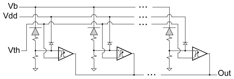
Circuit diagram for the pixel-level conditioning. Each passively quenched GPD pixel (shaded diode) triggers a comparator that is combined with a one-shot to produce a logic pulse with an externally set width. The logic pulses are summed to produce the SSPM output, labeled “Out”. Vb denotes the bias voltage, Vdd is the digital power, +5 V, and Vth is the global trigger threshold for the comparators.
The dependence of the DE on the excess bias, however, is not removed, thus some temperature dependence of the output is expected to remain at lower operating biases.
Figure 4a) shows the layout of the chip, referred to as the AE219 chip, fabricated to test the pixel-level signal conditioning. The 3mm × 3mm chip contains a 2 × 2 array of CMOS SSPM devices, however, only the first device, which correlates to the diagram illustrated in Figure 3 is described in this work. Figure 4b) shows the layout at the very center of the chip, where the four different pixel-level conditioning designs can be seen. The design described in this work is at the top left corner.
Figure 4.
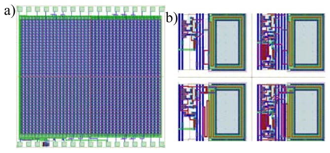
a) Layout of the AE219 chip with integrated components for pixel-level conditioning. b) Four designs illustrated in the zoom of the center of the chip. The designs include passive and active quenching of the pixel, however, only results from the passively quenched, conditioned pixel are presented in this work.
The pixels in the chip, which are the large rectangles in Figure 4b), are all p-on-n designs, similar to those used in the AE217. This GPD design electrically isolates the GPD pixel from the p-epi layer, and facilitates the integration of the signal conditioning.
The pixel-level-conditioning components described above are active. They contain MOSFETs and require a 5V power connection. The CMOS process used to make RMD’s SSPM devices also provides the capability of integrating passive components, such as a poly-silicon resistor network to divide the signal charge for position sensitivity.
2.3.2. Position-sensitive SSPMs for PET Imaging
Imaging applications, such as PET, require the determination of the location of the event. Position-sensitive detectors, such as PS-PMTs, and PS-APDs provide a mean to perform imaging with a limited number of signals, contacts and processing. In such devices, the signal charge is divided into four contacts, and the relative amplitude of the charge from each contact determines the location of the event.
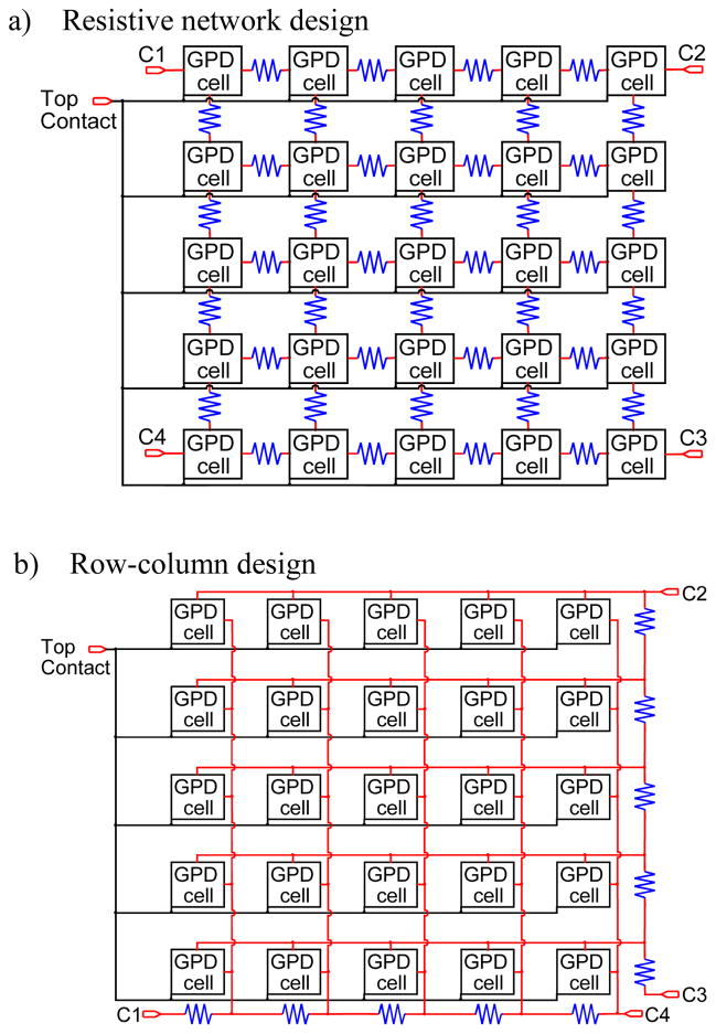
In this work, we present results from two of four designs. Figure 5 shows a circuit diagram for the two designs, which are denoted as a) the resistive network design, and b) the row-column design.
Figure 5.
a) Schematic of the “APD analog” resistor network for providing position information by dividing the charge into four contacts. The amount of charge in each contact is correlated to the location of the event. b) Schematic of the “row-column” charge-sharing network. In this design, the row and column signals are kept separate and independent of one another. The design utilizes fewer network resistors.
The resistive network design, a) is analogous to the expected circuit equivalent for PS-APDs. Equation (7) describes the calculation of the position from the signals at the four contacts [14].
| (7) |
To generate the images presented in this work, a single, additional scaling factor converts the signals to the image dimension, in mm.
The row-column design isolates the row signals from the column signals at each pixel through the passive quenching resistor. The value of the passive quenching resistor is orders of magnitude higher than the total resistance in the charge division chain connecting contacts C2 to C3 and C1 to C4. Therefore, equation (8) describes the calculation of the position from the contacts.
| (8) |
To correct for a slight pin-cushion distortion in the row-column design, the values for both X and Y, as calculated in Equation (8) above, were divided by dα, where d is |X|+|Y|, a measure of the distance from the origin, and α is an adjustable exponent with a value of ~0.1.
2.3.2.1. Simulations
The Resistive network design was modeled using H-spice. The purpose of the modeling was to determine the optimum value for the network resistor, in the context of using Equation (7) to calculate the location of the event. The model of the GPD element is an implementation of Cova et al. [15], the untriggered pixels were modeled with a simple capacitor. For simplicity, we modeled a 5 × 5 array of GPD pixels. The parameters for the Spice model of the GPD pixel [9], such as the breakdown voltage, junction capacitance, and “on resistance” are determined from GPD pixel characterization measurements.
2.3.2.2. PS-SSPM Prototype and Measurements
The designs illustrated in Figure 4, along with two other designs, were used to construct a 2×2 array of PS-SSPM devices, referred to as the AE218 chip. Figure 6 shows the layout for the prototype, which is a 3.2mm × 3.2mm chip.
Figure 6.
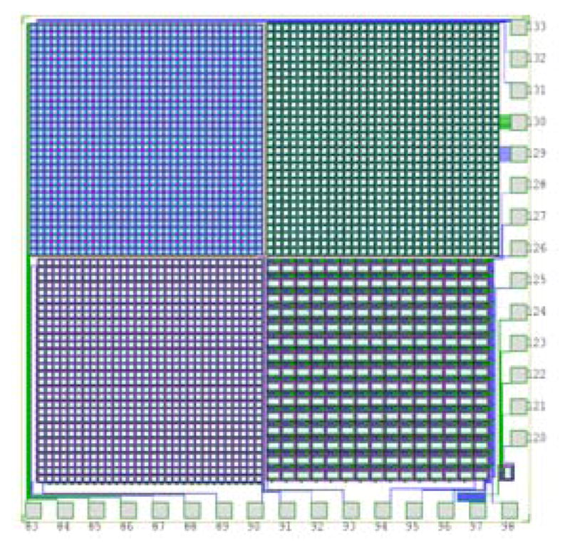
Layout of the PS-SSPM chip containing four different PS-SSPM devices, designated at the AE218 chip. Each device employs a different charge division design. The “APD analog” design is the top left device, and the “row-column” design is the bottom left device.
The resistive network PS-SSPM is the device at the top left corner of the 2×2 array, and the row-column PS-SSPM is the device at the bottom left corner. The fill factor of the resistive network PS-SSPM is 46%, and the fill factor of the row-column PS-SSPM is 41%. The GPD pixels are the p-on-n elements used in the previous designs described in this work, and have an active area of 30μm × 30μm.
The performance of the PS-SSPM detectors were characterized by placing a segmented scintillation material on the device, coupled with optical grease, and irradiating with a flood-field of gamma rays from a selected source. Standard nuclear detection electronics were connected to each of the four readout contacts. The selected integration times depended on the scintillation material in the segmented scintillation detector. Figure 7 shows a photograph of the segmented scintillation detectors superimposed with the layout of the PS-SSPM.
Figure 7.

(left) Segmented CsI scintillation crystal used to characterize the “APD analog” PS-SSPM detector, placed on dime for scale. Only 3×3 scintillation segments sit atop of the PS-SSPM detector, as indicated by the dashed boxes. A magnified image of the SSPM device is labeled “×10”. The segmented LYSO scintillation crystal (right) used to characterize the “row-column” PS-SSPM detector. As with the CsI, only 3×3 scintillation segments sit atop of the PS-SSPM device, which is on of the four devices on the chip.
The scintillation detector on the left, a), is CsI (Tl) that has a segment size of 300 μm×300μm on a pitch of 450 μm. The scintillation detector on the right, b) is LYSO, with a segment size of ~450μm×450μm on a pitch of 500 μm. As indicated in the figure, only a 3×3 piece of the segmented scintillation segment will sit atop of the 1.5 mm × 1.5 mm PS-SSPM.
3. Results and Discussion
3.1. Calibration of gamma-ray spectra
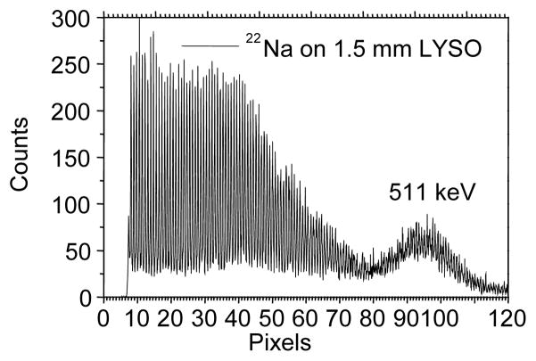
The plot at the top of Figure 8 shows the raw spectrum measured from a 441-element SSPM, coupled to an LYSO scintillation crystal, irradiated with 22Na. The x-axis shows the signal calibrated against the approximate number of pixels triggered. The plot on the bottom shows the same spectrum plotted against the energy of the gamma-rays, where the 511-keV peak and 1275 keV peak were used for the calibration. In the corrected spectrum, the 511-keV peak is smaller than the Compton and escape features, as expected for small scintillation crystal. The relative magnitude of the 1275-keV peak is also much smaller in the “corrected” spectrum, again, consistent with the 1.5mm × 1.5mm × 3mm scintillation crystal.
Figure 8.
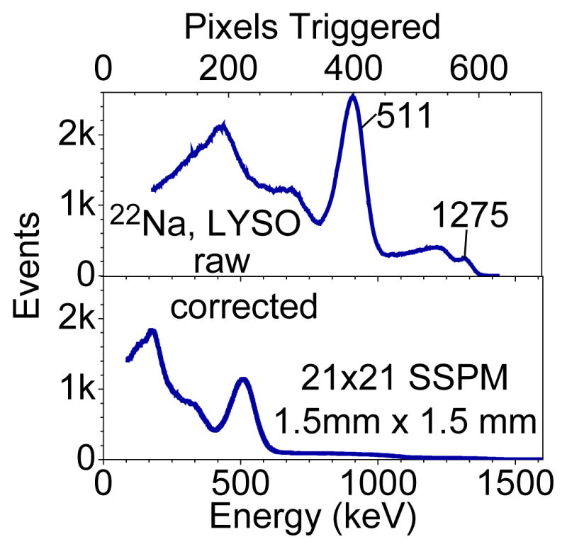
Plot of the raw gamma-ray spectrum from a 1.5mm × 1.5mm × 3 mm LYSO crystal irradiated with 22Na in units of pixels triggered (top). The 511-keV and 1275-keV peaks are labeled to illustrated the non-linearity of the energy scale. Note that the number of pixels triggered exceeds the number of pixels in the SSPM because a shaping time of 250 ns was used in the measurement. The corrected energy spectrum (bottom) for the scintillation detector. The image in the background is the SSPM detector.
In the top plot, the intense signal for the 1275-keV peak exceeds the number of pixels in the SSPM by triggering pixels multiple times during the integration period.
In the top plot, the intense signal for the 1275-keV peak exceeds the number of pixels in the SSPM by triggering pixels multiple times during the integration period.
The corrections are necessary for determining the energy resolution when then number of triggered pixels exceeds ~40% of the pixels in the device. For large are devices, the corrections and non-linearity become less important as the number of pixels in the device increases relative to the number of photons generated in the scintillation pulse.
3.2. Energy resolution simulations
The energy resolution simulations examine the effect of the number of SSPM pixels, as well as other SSPM characteristics, on the expected energy resolution performance. Figure 9 shows the expected energy resolution for a 511-keV photo-peak in LYSO for different magnitudes of dark counts and excess noise as a function of the SSPM size, scaled to the linear length of the device in pixels.
Figure 9.
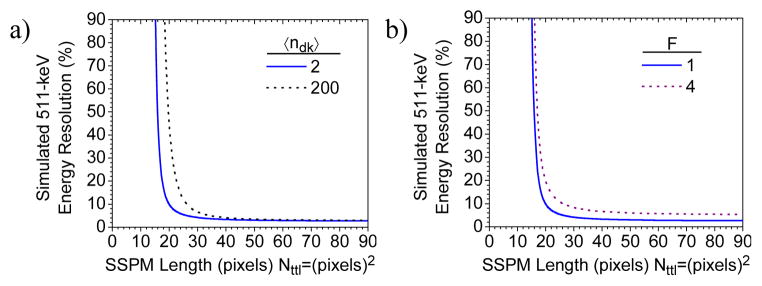
a) Simulated effect of the average number of dark count on the energy resolution of an SSPM with an LYSO scintillation crystal measuring the 511-keV peak as a function of the size of the SSPM detector. Notice that the effect of the dark counts is greatly exaggerated, and most pertinent for small SSPM detectors. b) The simulated effect of the excess noise on the energy resolution, which adversely affects all sizes of SSPM detectors.
For the 511-keV photo-peak, the dark counts have a dramatic effect on the energy resolution for small SSPMs, and the effect approaches the asymptotic Poisson limit when the number of pixels approach infinity. Obviously, the dark counts also affects the noise floor of the detector, as well as the energy resolution. As expected, the excess noise factor degrades the energy resolution performance for all SSPM sizes. This data shows that the results are consistent with expectations, especially in the asymptotic Poisson limit when the number of pixels approach infinity.
Figure 10 shows a plot of the expected energy resolution for the 511-keV photo-peak as a function of SSPM size for three different values of the DE, which can be experimentally achieved by adjusting the excess bias.
Figure 10.
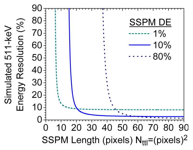
Plot of the simulated energy resolution of different sized SSPM detectors with an LYSO scintillation crystal measuring the 511-keV peak at three different SSPM detection efficiencies, which correlate to three different operating voltages. Notice that the degradation in energy resolution performance is appreciable for small SSPM detectors with a high detection efficiency.
Interestingly, the energy resolution of a small SSPM device can be improved by reducing the detection efficiency. In other words, the better the DE of the SSPM, the more pixels are needed to achieve the optimum energy resolution performance. Again, the asymptotic limit with the size of the SSPM behaves as expected.
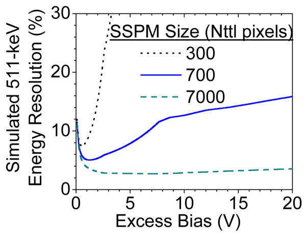
Figure 11 uses the experimental dependences of the DE, DCR, and F on Vx to estimate the dependence of the energy resolution performance on the excess bias for a 511-keV photo-peak with three array sizes.
Figure 11.
Simulated plot of the best operating voltage for three different sizes of SSPM detectors when measuring the scintillation light from an LYSO crystal at 511-keV. Notice that the binomial statistics associated with the SSPM detector limit the energy resolution performance at high excess biases, especially for SSPM devices with a small number of pixels, see the curve for nttl=300.
As indicated in the plot, the best operating voltage for small CMOS SSPM devices, similar to the AE217, is expected to be less than 5 volts. In fact, the energy resolution performance of a 441-pixel SSPM contains a substantial contribution from the binomial statistics associated with the number of triggered pixels, which is different from the energy resolution expected for Poisson statistics. Of course, the plot does not include contributions from the scintillation material, which can be >9% for LYSO at 511-keV.
3.3. CMOS SSPMs with integrated circuits
Two prototypes, designated at the AE219 and AE218 were fabricated with integrated circuit components.
3.3.1. Pixel-level conditioning
Figure 12 shows a photograph of the 3.2mm×3.2mm chip, the AE219, with pixel-level signal-conditioned SSPM detectors.
Figure 12.
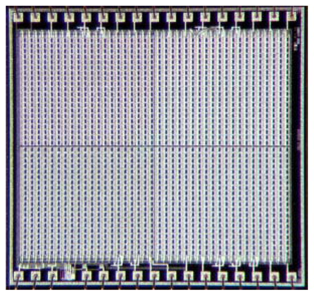
Photograph of the 3.2mm × 3.2mm AE219 chip fabricated with pixel-level signal conditioning. The chip contains four different SSPM devices. The 1.5mm × 1.5mm device tested in this work is at the upper left corner of the photograph. The fill factor of all the SSPM devices is ~25%.
The fill factor of all of the SSPM devices in this chip is ~25%, and each of the four devices contain 400 pixels. Figure 13 shows a plot of the pulse amplitude histogram measured with the pixel-level signal-conditioned SSPM when illumined with a pulsed LED at six different intensities.
Figure 13.
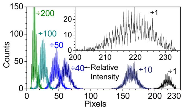
Plot of the pulse amplitude distributions for the pixel-conditioned SSPM detector illuminated with a pulsed LED at 7 different intensities, labeled “÷200” to “÷1”. The strongest light pulse is labeled “÷1”. Notice the resolution of the multiplicity in the number of pixels triggered by the LED pulse, which is the fine structure illustrated in the expanded plot at the upper right corner.
The fine structure in the histogram plot is the resolution of the pixel multiplicity out to amplitudes as large as 220 detected photons, i.e. 220 GPD pixels triggered. Notice the non-linearity in the response of the SSPM as the light pulse amplitude is decreased from “÷1” to “÷10”.
Figure 14 shows a plot of the spectrum from the same SSPM device when coupled to an LYSO scintillation crystal irradiated with a 22Na source. Given an estimate of the incident number of photons in the scintillation, the detection efficiency of the SSPM can be readily assessed from the spectrum since ~100 pixels are triggered by the 511-keV event. The excess bias used for these measurements is less than 1V, which results in the low DE.
Figure 14.
Plot of the gamma-ray spectrum from a 1.5mm × 1.5mm × 1.5 mm LYSO crystal irradiated with 22Na. Notice the resolution of the individual pixel multiplicity in the spectrum. Since each 511-keV event creates ~15,000 photons, we can readily see that the detection efficiency of the SSPM is less than 1%.
The following two factors dominate the energy resolution performance: the relatively low DE, <1%, and the small size of the device, 400 pixels. Because of the small size of the device, however, the excess bias, and detection efficiency must be low to optimize the energy resolution. This data shows that pixel-level signal processing preserves the effective digitization of the scintillation pulse by the SSPM detector, and It also it provides a convenient mechanism to incorporate the shaping time for different scintillation materials. Performance benefits of preserving the digitization, however, have yet to be demonstrated.
3.3.2. Position-sensitive SSPMs for PET Imaging
We characterized the performance of PS-SSPMs in terms of the clarity of the image (the ability to resolve scintillation segments). We also characterized the energy resolution performance of the “:row-column” position-sensitive SSPM detector.
3.3.2.1. Simulation Results
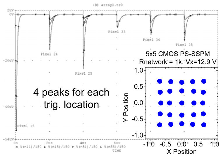
Figure 15 shows the simulated output from all four contacts on the resistive network SSPM for 6 different events, where each “peak” is the amplitude of the signal for a contact when a single pixel in the 5×5 array is triggered.
Figure 15.
SPICE Simulation results for the Geiger pulses divided onto the four contacts of the PS-SSPM. Each peak is labeled with the pixel that was triggered, e.g., the peak(s) labeled “pixel 15” contain 4 peaks, one at each contact, that were produced when the GPD pixel in the first row, fifth column was triggered. In this example, three of the peaks have an amplitude of ~0uV, and one of the contact has an amplitude of ~50 uV. The plot at the lower right corner shows the image that was reconstructed with the peak amplitudes at each contact using a network resistor of 1k.
The first peak, at time 0, corresponds to the signals at the four contacts when the pixel in row 5, column 1 is triggered. This is a corner pixel, so only one contact contains any appreciable signal amplitude; the amplitudes at the other contacts are zero.
The plot in the lower right corner of Figure 15 shows the image reconstructed from the contact amplitudes when the value of the network resistor is 1k. Figure 16 shows the reconstructed images for network resistor values of 50k and 150 Ohms. Although the images exhibit distortions, these distortions are specific to the use of Equation (7) to generate the image. From the simulations results, we determined that the optimum network resistor value is ~5k. We designed and fabricated the PS-SSPM using this resistor value.
Figure 16.
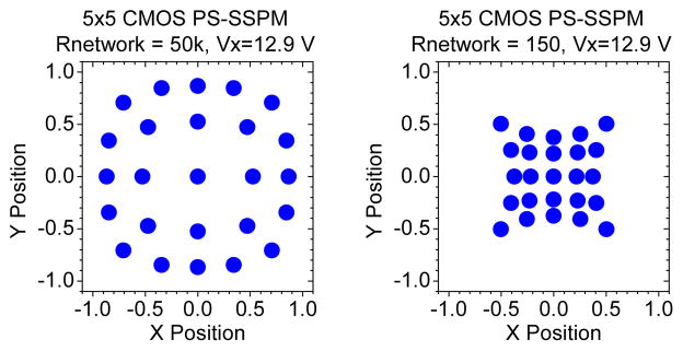
Plot of images reconstructed from the SPICE simulations with 50k network resistors and 150-Ohm network resistors. Notice the transition from a barrel to pincushion distortion depending on the network resistor value.
3.3.2.2. Prototype Results
Figure 17 shows a photograph of the 3.2mm × 3.2mm PS-SSPM chip, designated as the AE218 chip.
Figure 17.
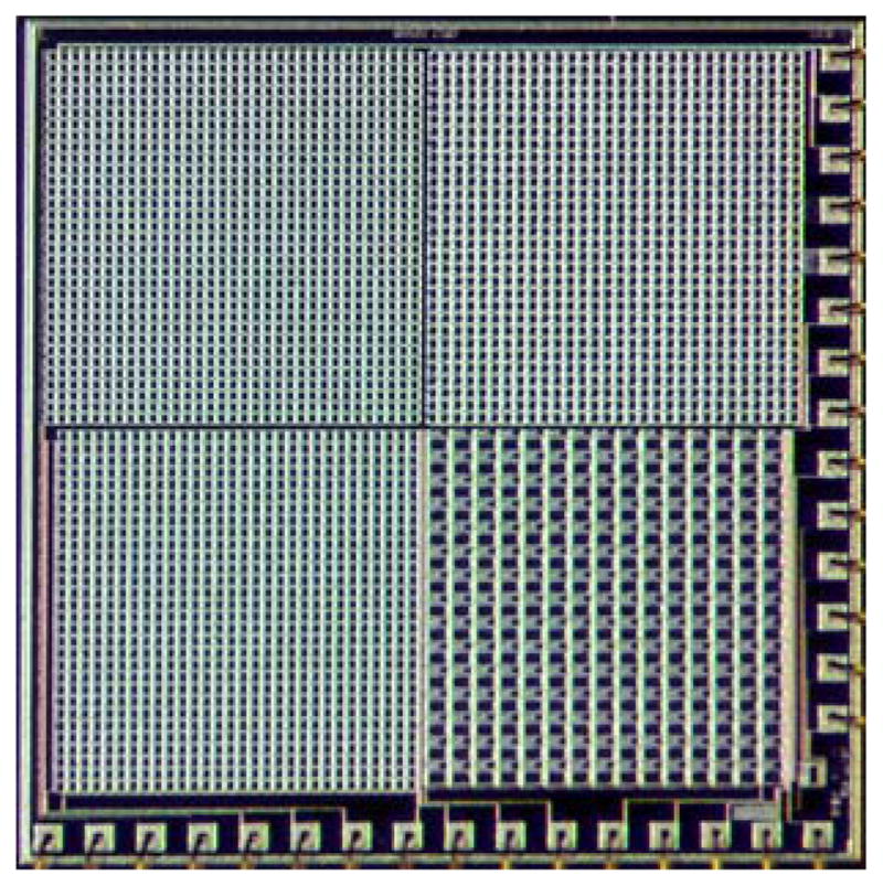
Photograph of the 3mm × 3mm PS-SSPM chip, containing a 2×2 array of different PS-SSPM devices. The “PS-APD analog” is the 1.5mm × 1.5 mm device at the top left, and the “row-column” device is on the bottom left.
The prototype is a 2×2 array of PS-SSPM devices. The resistor network design is at the top left corner in the photograph, and the row-column design is in the bottom left corner. The size of each PS-SSPM is 1.5mm × 1.5 mm. The resistor network PS-SSPM contains 1089 p-on-on pixels that are 30μm × 30μm. The row-column PS-SSPM contains 900 p-on-n pixels that are also 30μm × 30μm.
Figure 18 shows the image reconstructed from the flood-field irradiation of the segmented CsI(Tl) array coupled to the resistor-network SSPM with 137Cs using Equation (7). The plot shows the image of the 3×3-scintillation array that sits atop of the resistive-network PS-SSPM.
Figure 18.
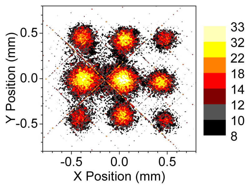
Reconstructed image from the flood-field illumination of the segmented CsI scintillation crystal, coupled to the “PS-APD analog” PS-SSPM with a 137Cs source. Notice the resolution of the 3×3 array of scintillation segments, and the absence of distortions, in agreement with the reconstructed image from the simulation.
The measured reconstruction agrees with the simulated reconstruction shown in the bottom right corner of Figure 16. Notice, however, that the image from the scintillation segments is not square, as might be expected from their geometric shape.
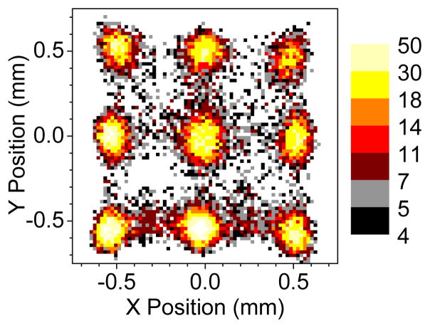
Figure 19 shows the image reconstructed from the flood-field irradiation of the segmented LYSO array coupled to the resistor-network SSPM with 22Na using Equation (8). The location of the 3×3-scintillation segments is accurately reproduced, however, the shape of the images exhibit slight distortions compared to the round images in from Figure 18. The inactive space in the segmented LYSO scintillation array is much smaller than that in the CsI(Tl) array.
Figure 19.
Reconstructed image from the flood-field illumination of the segmented LYSO scintillation crystal, coupled to the “row-column” PS-SSPM with a 22Na source. Notice the resolution of the 3×3 array of scintillation segments, and the absence of distortions,
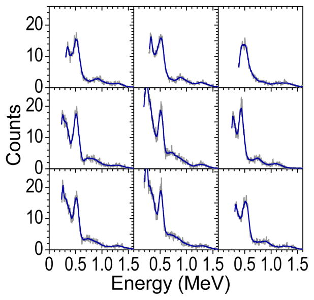
The PS-SSPM also provides the capability of resolving the energy associated with each event. Binning the events according to their location in a 3×3 grid produce the spectra shown in Figure 20. The spectra have been calibrated according to the prescription described in this work.
Figure 20.
Plot of the energy spectra associated with each of the LYSO scintillation segments, clearly resolving the 511-keV and 1275-keV peaks for most of the segments. As a position-sensitive detector, the “effective” number of pixels associated with each scintillation segment likely limits the measured energy resolution.
The 511-keV peak and the 1275-keV peak can be distinguished in most of the spectra. The energy resolution is surprisingly good considering that the effective SSPM size for each scintillation segment is approximately 100 pixels, or less considering the distribution of light in the segment.
These images and spectra show that the PS-SSPM devices are suitable for medical imaging applications, such as PET, especially in applications involving magnetic fields, such as PET-MRI imaging.
4. Summary and Conclusions
This work shows that the energy resolution performance of SSPM devices is affected by the number of pixels due to the binomial nature of the statistics associated with the triggered pixels. The work also demonstrates that pixel-level signal conditioning preserves the inherent digitization of the SSPM detector. We have also shown that the measurements of the PS-SSPM devices agree with the SPICE simulations, with respect to selecting the network resistor that minimized the distortions, and that such devices provide imaging capabilities suitable for PET applications.
Acknowledgments
We would like to acknowledge stimulating and fruitful interactions with Prof. David Wehe and Paul Barton at the University of Michigan. We would also like to acknowledge support by DTRA, DNDO and NIH for supporting various parts of this effort.
References
- 1.Shah KS, Glodo J, Moses WW, Derenzo SE, Weber MJ. LaBr3:Ce Scintillators for Gamma-Rray Spectroscopy. IEEE Trans Nucl Sci. 2003;50:2410. [Google Scholar]
- 2.Shah KS, Glodo J, Higgins W, van Loef EVD, Moses WW, Derenzo SE, Weber MJ. CeBr/sub 3/ scintillators for gamma-ray spectroscopy. IEEE Trans Nucl Sci (USA) 2005;52:3157–9. [Google Scholar]
- 3.Glodo J. Scintillation Properties of 1 Inch Cs2LiYCl6:Ce Crystals. IEEE Transactions Nuclear Science. 2008;55:12060–1209. [Google Scholar]
- 4.McIntyre RJ. On the avalanche initiation probability of avalanche diodes above the breakdown voltage. IEEE Trans Electron Devices (USA) 1973;ED20:637–41. [Google Scholar]
- 5.Zappa F, Lacaita AL, Cova SD, Lovati P. Solid-state single-photon detectors. Opt Eng, Bellingham (USA) 1996;35:938–45. [Google Scholar]
- 6.Vasile S, Gordon JS, Farrell R, Squillante MR. Fast avalanche photodiode detectors for the Superconducting Super Collider. Semiconductors for Room-Temperature Radiation Detector Applications Symposium. 1993:537–42. [Google Scholar]
- 7.Buzhan P, Dolgoshein B, Filatov L, Ilyin A, Kantzerov V, Kaplin V, Karakash A, Kayumov F, Klemin S, Popova E, Smirnov S. Silicon photomultiplier and its possible applications. NIM A. 2003;504:48–52. [Google Scholar]
- 8.Jackson JC, Phelan D, Morrison AP, Redfern RM, Mathewson A. Toward integrated single-photon-counting microarrays. Opt Eng, Bellingham (USA) 2003;42:112–18. [Google Scholar]
- 9.Christian JF, Svolos G, Kogan AI, Augustine FL, Squillante MR, Entine G. Characterization & Modeling of APD Pixels Made with CMOS Technology. presented at Nano Materials for Devense Applications; Maui, HI. [Google Scholar]
- 10.Johnson EB, Barton P, Shah KS, Stapels CJ, Wehe DK, Christian JF. Energy Resolution in CMOS SSPM Detectors Coupled to an LYSO Scintillator. IEEE Transactions Nuclear Science. 2009;56:1024. [Google Scholar]
- 11.Pepin CM, Bernard P, Perrot A-L, Pepin C, Houde D, Lecomte R, Melcher CL, Dautet H. Properties of LYSO and Recent LSO Scintillators for Phoswich PET Detectors. IEEE Trans Nucl Sci. 2004;51:789. [Google Scholar]
- 12.Buzhan P, Dolgoshein B, Filatov L, Ilyin A, Kantzerov V, Kaplin V, Karakash A, Kayumov F, Klemin S, Popova E, Smirnov S. Silicon photomultiplier and its possible applications. Nuclear Instruments and Methods in Physics Research Section A: Accelerators, Spectrometers, Detectors and Associated Equipment Proceedings of the 3rd International Conference on New Developments in Photodetection. 2003;504:48–52. [Google Scholar]
- 13.Stapels C, Lawrence WG, Squillante MR, Entine G, Augustine FL, Christian J. The Solid-state Photomultiplier for an Improved Gamma-ray Detector. presented at IEEE Conference on Technologies for Homeland Security (1105); April 26–28; Boston, MA. [Google Scholar]
- 14.Zhang J, Foundray AMK, Olcott PD, Levin CS. Performance characterization of a novel thin position-sensitive avalanche photodiode-based detector for high resolution PET. IEEE Nuclear Science Symposium Conference Record. 2005;5:2478–2482. [Google Scholar]
- 15.Cova S, Ghioni M, Lacaita A, Samori C, Zappa F. Avalanche Photodiodes and quenching circuits for single-photon detection. Applied Optics LP. 1996;35:1956. doi: 10.1364/AO.35.001956. [DOI] [PubMed] [Google Scholar]


