

Abstract
Purpose:
Silicon photodetectors are of significant interest for use in positron emission tomography (PET) systems due to their compact size, insensitivity to magnetic fields, and high quantum efficiency. However, one of their main disadvantages is fluctuations in temperature cause strong shifts in gain of the devices. PET system designs with high photodetector density suffer both increased thermal density and constrained options for thermally regulating the devices. This paper proposes a method of thermally regulating densely packed silicon photodetectors in the context of a 1 mm3 resolution, high-sensitivity PET camera dedicated to breast imaging.
Methods:
The PET camera under construction consists of 2304 units, each containing two 8 × 8 arrays of 1 mm3 LYSO crystals coupled to two position sensitive avalanche photodiodes (PSAPD). A subsection of the proposed camera with 512 PSAPDs has been constructed. The proposed thermal regulation design uses water-cooled heat sinks, thermoelectric elements, and thermistors to measure and regulate the temperature of the PSAPDs in a novel manner. Active cooling elements, placed at the edge of the detector stack due to limited access, are controlled based on collective leakage current and temperature measurements in order to keep all the PSAPDs at a consistent temperature. This thermal regulation design is characterized for the temperature profile across the camera and for the time required for cooling changes to propagate across the camera. These properties guide the implementation of a software-based, cascaded proportional-integral-derivative control loop that controls the current through the Peltier elements by monitoring thermistor temperature and leakage current. The stability of leakage current, temperature within the system using this control loop is tested over a period of 14 h. The energy resolution is then measured over a period of 8.66 h. Finally, the consistency of PSAPD gain between independent operations of the camera over 10 days is tested.
Results:
The PET camera maintains a temperature of 18.00 ± 0.05 °C over the course of 12 h while the ambient temperature varied 0.61 °C, from 22.83 to 23.44 °C. The 511 keV photopeak energy resolution over a period of 8.66 h is measured to be 11.3% FWHM with a maximum photopeak fluctuation of 4 keV. Between measurements of PSAPD gain separated by at least 2 day, the maximum photopeak shift was 6 keV.
Conclusions:
The proposed thermal regulation scheme for tightly packed silicon photodetectors provides for stable operation of the constructed subsection of a PET camera over long durations of time. The energy resolution of the system is not degraded despite shifts in ambient temperature and photodetector heat generation. The thermal regulation scheme also provides a consistent operating environment between separate runs of the camera over different days. Inter-run consistency allows for reuse of system calibration parameters from study to study, reducing the time required to calibrate the system and hence to obtain a reconstructed image.
Keywords: avalanche photodiode (APD), position sensitive avalanche photodiode (PSAPD), positron emission tomography (PET), positron emission mammography (PEM), temperature
1. INTRODUCTION
Silicon photodetectors for use within positron emission tomography (PET) systems are currently an active area of research1,2 as their compactness, quantum efficiency,3 and MR compatibility4,5 are advantageous over conventionally used photomultiplier tubes (PMTs). The devices most commonly investigated for use within PET are the avalanche photodiode (APD) and the silicon photomultiplier (SiPM), which is sometimes referred to as a Geiger mode avalanche photodiode (GAPD),3,6 along with their position sensitive variants: including the position sensitive APD (PSAPD)7 and the position sensitive SiPM (PS-SiPM).8 The main disadvantage of silicon-based photodetectors is that the gain of the devices is sensitive to thermal changes. It has been shown, for instance, that PSAPDs can experience a gain variation of 6.8% °C−1 at room temperature,9 and SiPMs can show up to a 5% °C-1 shift in gain.10 Silicon photodetectors must also deal with the degradation of their SNR by dark currents due to thermal generation of carriers which increases exponentially with temperature.11–13 To overcome these disadvantages, commonly, both temperature compensation techniques,14–16 as well as thermal regulation systems to keep the detectors at or below room temperature,17 have been employed.
Another drawback of silicon photodetectors is that these detectors are difficult to manufacture in large areas. In contrast to PMTs, which can be manufactured with larger sensitive areas, these silicon-based detectors must be tiled together to cover volumes of scintillation crystals relevant for clinical or preclinical imaging.18 Many multiplexing methods have been explored to achieve larger effective areas without increasing the readout complexity.19,20 A greater number of devices packed into a smaller area, however, poses a greater thermal regulation challenge. When these detectors are used as a part of a PET system, thermal regulation is further complicated by both the heat output from the devices and from neighboring circuitry. This can cause instability in the performance of the detectors,12 as well as in the performance of the system as a whole. Keerman et al. investigated the effects of temperature on the LabPET system and showed there is degradation in the image quality at higher temperatures and suggested methods to compensate for these variations.21 There is, however, continued discussion on the best methods of measuring and compensating for temperature in these complex systems.22
The concerns about thermal regulation are especially relevant in the case of a novel, 1 mm3 resolution, high-sensitivity clinical PET camera that is being constructed in our lab.23 This system takes advantage of a novel, thin PSAPD (Refs. 24 and 25) to stack the detectors vertically so that radiation enters the camera edge-on, i.e., from the side of the crystal arrays, as seen in Fig. 1, while maintaining high crystal packing fraction. Each PSAPD within this stack is coupled to an 8 × 8 array of 1 mm3 LYSO crystals.25 The system is designed to use 4608 PSAPDs, with 2304 placed in each of two imaging heads, one of which can be seen in Fig. 2. This design, with one usage concept shown in Fig. 2, enables high photon sensitivity over the region of interest and allows flexibility in positioning of the imaging heads. The heat generated within the front-end (approximately 4 W) needs to be dissipated to maintain optimum operation. An additional challenge in this tightly packed design is that there are limited possibilities to directly regulate the temperature of the PSAPDs.
FIG. 1.

Each detector “dual-module” contains two PSAPD–LYSO detectors. One placed close to the imaging target and one placed immediately behind the other. Shown are 24 dual-modules, with the PSAPDs located underneath each of the crystal arrays. In this arrangement, the 511 keV photons enter the crystal arrays edge-on, allowing intrinsic 3D positioning of one or more interaction positions per incoming photon, however, these densely packed PSAPDs present a difficult cooling challenge.
FIG. 2.

On the top is a rendering of the design of each imaging head, composed of a stack of tiled LYSO–PSAPD dual-modules in an angled section in the front of the head. Every eight layers of dual-modules are connected to a layer of circuit boards that perform signal conditioning, provide bias voltage, measure leakage current, and acquire data. Cooling pipes for the circuit board layers can be seen at the edge of the imaging head. The two heads shown on the bottom are placed on the sides of the breast. The design allows for both high photon detection sensitivity as well as flexibility to physical position each head in 3D space around the patient.
In this paper, we build on the method initially presented by Zhai et al.26 for regulating the temperature of these densely packed silicon photodetectors within this PET camera. While this paper presents methodologies in the context of our system under development, the techniques presented are of interest to developers of imaging systems that employ a large number of semiconductor devices, as this technique uses careful control of large-area temperature regulation elements to provide stability to all of the individual detector modules. In Sec. 2, we characterize the properties of this thermal design. In Sec. 3, these properties are utilized in the design of a control system to provide consistent operation of the PSAPDs. Results are then presented from experiments carried out to verify the functionality of this control design.
2. HARDWARE DESIGN AND CHARACTERIZATION
2.A. Thermal regulation design
Due to the tight packing of detectors, the thermal regulation for the APDs is not trivial. We chose an approach where heat is drawn to the edge of the detector fins, as seen in Fig. 3. The system is cooled by Peltier elements located outside of a 2.54 mm tungsten alloy shielding layer27 and an aluminum sidewall. Peltiers are thermoelectric devices across which a thermal gradient is created when an electric current is applied. The gradient is proportional to current.28 When used for cooling, the hot side of the Peltiers must be cooled by a heat sink. In this design, the heat is drawn away by a water-cooled heatsink. The chiller (Thermotek RC series) used for the water cooling has a cooling capacity of 610 W at a water temperature of 20 °C. A rendering of the front-end of the camera, with the various parts broken out, can also be seen in Fig. 3.
FIG. 3.

Shown on the top is the thermal pathway for heat generated by the APDs (top grid) in one layer of the stack shown in Fig. 2. Aluminum nitride windows (not shown) surround the crystal arrays, support the APDs, and draw heat to an aluminum bar. The aluminum bar (center metal strip) acts as a conduit to draw heat from the center of the fin to the sidewalls of the fin. The sidewalls are connected to thermoelectric elements (Peltiers) that are cooled by chilled-water regulated heatsinks. The water chiller used to cool the heatsinks provides baseline cooling, while the Peltiers provide faster control. Shown in the center of the aluminum bar is the location of the thermistor, which is used to measure the temperature of each fin. A rendering of the thermal regulation design, seen from the front of the active imaging region, is shown on the bottom.
2.B. Leakage current and temperature measurement
The PSAPDs are packaged into a physical unit of two PSAPDs that is referred to as a dual-module. The leakage currents from both PSAPDs are read out collectively by amplifying and inverting the voltage drop over a known resistance using an AD822 op-amp.29 The op-amp accepts signal voltages below its negative rail voltage of 0 V, and scales it to a positive voltage that is subsequently read by an ADC channel on an ATmega16A microcontroller as shown in Fig. 4. This design eliminates the need to provide a −5 V power supply connection to the system, simplifying the power distribution design significantly. Current values for all of the modules are read at a rate of 10 Hz over USB running at 2 MBaud and displayed to the operator using a custom graphical user interface in quasi real-time. The core temperature of each row of PSAPDs is monitored using a thermistor whose output is measured by the same microcontroller using a thermistor temperature-to-pulse-width converter (MAX6691) and displayed using the same interface. The temperature measurement has a resolution of 0.005 °C.
FIG. 4.

A block diagram of the circuitry required to measure the leakage current from each dual-module of PSAPDs.
The bias voltage to the modules (typically around −1740 V) is controlled primarily by an external high voltage power supply which also provides a measure of the total leakage current of all of the PSAPDs. The supply is capable of providing a stable voltage within 10 mV pp.30 A positive bias is individually added for each module using a DAC chip (AD5535) that reduces the reverse bias by a programmed value between 0 and 92 V. This individual distribution system has a ripple voltage of 20 mV pp.29
2.C. Characterization methods
Simulations with this thermal regulation system have shown that the PSAPDs within the center of the camera will operate at a temperature approximately 3 °C higher than the temperature of the PSAPDs closest to the Peltier elements at the edge of the camera.26 The temperature of the PSAPDs cannot be measured directly due to the tight construction of the camera. It has been demonstrated, however, that there is a linear relationship between temperature and bias voltage for a constant PSAPD gain. This relationship, seen in 1.7 V °C−1, seen in Fig. 12 of Vandenbroucke et al.,9 means that if a PSAPD is cooled an additional 1 °C then the bias voltage must be reduced 1.7 V to keep the same gain. The factor of 1.7 V °C-1 was measured on one device. PSAPDs may have variations around this value, but these differences are mitigated by averaging across multiple devices in the same position relative to the center. This relationship allows a relative temperature difference from thermal equilibrium to be measured by finding a voltage at which the gain of the cooled PSAPD equals the gain of the uncooled PSAPD. To accomplish this, the gain of the PSAPDs is measured by analyzing the 511 keV photopeak position at thermal equilibrium without cooling and with a high reverse bias voltage (−1750 V). The cooling is then activated and the gain of the PSAPDs is measured at several lower voltages (from −1729 to −1745 V in 2 V steps). There will be a voltage for which the gain of the cooled PSAPDs is equal to its unregulated gain. The relative temperature change for each PSAPD can then be inferred.
As previously mentioned, the thermistor for each row of PSAPDs is located within the center of the row (see Fig. 3). Changes in cooling on the edge of the camera will have a delay before they are registered as a change in temperature by the thermistor because of the distance of the thermistor from the Peltiers. The heat capacity of the device causes this notable delay. A study was developed to characterize the time that thermal changes require to propagate through the device. For this experiment, an abrupt change in the Peltier current is made. The time between this change and then a drop in each module’s leakage current is measured. The leakage current of the PSAPDs is very sensitive to changes in temperature and provides a fast and direct measurement of the thermal propagation.
2.D. Characterization results
The resulting temperature profile across the PSAPDs of the camera, as seen on the left in Fig. 5, confirms the simulations presented in Zhai et al.26 The PSAPDs in the center of the camera experience a temperature that is 3.5 ± 0.3 °C and 3.3 ± 0.4 °C higher than those at the edge for the left and right imaging heads, respectively. There is an asymmetry between the left and right side in the plot shown in Fig. 5 of 0.7 ± 0.5 °C and 0.8 ± 0.5 °C for the two imaging heads, respectively. This may be due to a thermal coupling difference between the heatsinks or other mechanical inconsistencies. This does not adversely affect the performance of the system, as the effects of the asymmetry are calibrated out of the system by correcting for the gains of the individual PSAPDs. The thermal propagation delay profile can be seen on the right in Fig. 5. Changes in cooling at the edge of the imaging head require 149 ± 5 s to be observed by the PSAPDs in the center of the camera.
FIG. 5.

Averaging over eight rows of PSAPDs for each imaging head, the measured difference between the edge and the center of the camera, shown on the top, was 3.5 ± 0.3 °C and 3.3 ± 0.4 °C for the left and right imaging heads, respectively (256 PSAPDs each). On the bottom, the average propagation time required for a change in cooling to reach a module position (column) in the rows of 16 PSPAD dual-modules is shown. The average time for a thermal change to propagate to the center of the fin is 149 ± 5 s. The current of both the front and back PSAPD is measured jointly, so this represents the time for a response to be seen in the total for both PSAPDs.
3. CONTROL DESIGN AND CHARACTERIZATION
3.A. Temperature control design
As mentioned previously, temperature fluctuations contribute to shifts in the gain of the PSAPDs. This directly affects the energy resolution of the camera. We aim to keep the contribution of thermal fluctuations to less than 1% of the energy resolution. This goal requires maintaining a constant temperature to within ±0.15 °C as the gain of the PSAPDs increases to 6.8% °C-1 at 18 °C. This fluctuation of the PSAPD gain is calculated from a linear approximation to the gain curve reported in Fig. 12 of Vandenbroucke et al. at 18 °C.9 For this study, we have set a conservative target of maintaining a constant system temperature within ±0.10 °C of 18 °C. The operating point of 18 °C was chosen as to operate the PSAPDs below room temperature with only moderate water chiller power requirements.
The temperature stability goal that we have set is not achievable when the chiller and Peltier elements are operated without any active feedback control. Without such control, the system temperature drifts with the ambient temperature, which can easily drift several degrees due to heat emitted by the readout electronics. Therefore, we investigated methods of controlling the temperature by actively adjusting the Peltier current. A proportional-integral-derivative (PID) control implementation was chosen for its ability to handle a broad set of control scenarios through the tuning of its parameters and its straight-forward implementation in software. A simple PID loop, diagrammed in Fig. 6, uses the difference between the target temperature and the measured temperature to calculate the current that should be set for the Peltiers. The value of the error, its derivative, and the integral of the error over time each contribute to the output based on operator-tuned parameters (the P, I, or D shown in Fig. 6).
FIG. 6.

On the left is a block diagram of a PID loop that controls the system based upon average fin temperature. The value of the difference in temperature as well as its integral and derivative is multiplied by their respective gains (P, I, or D), and summed together to specify the current of the Peltiers. On the right is a description of the cascaded PID loop system used to provide stability for both leakage current and temperature. The leakage current loop provides a stable operating point for the system. The set point for this loop is then calibrated using the thermistor data in a secondary control loop.
The basic feedback design, when used in this PET camera, is able to remove any correlation between the system temperature and ambient temperature, and thus maintain stability around a constant temperature. However, residual temperature variations larger than the design goal were still observed using this simple PID loop. These variations are a result of the propagation delay between changes in cooling on the edges of the system, shown in Fig. 5. Large values of P, I, and D within the PID loop tend to overcompensate the amount of cooling needed prior to the system registering a change in temperature. Small values of P, I, and D prevent this overcompensation, but result in a drift in fin temperature with respect to ambient temperature.
To provide a more robust solution for control around a given operating point, the same style of PID loop shown in Fig. 6 can be used with a target total leakage current as the main parameter instead of temperature. A control loop utilizing total leakage current is both able to reduce the local fluctuations to within the desired range while also remaining independent of ambient temperature. This method has the disadvantage of not being uniquely correlated to the gain of the PSAPDs or to their temperature. To provide a controlled temperature, the leakage current control loop’s target is then set by a second PID loop that uses the system temperature, as shown in Fig. 6. In this design, the leakage current provides the primary stability for the system, by tapering fluctuations around the targeted operating point, while the outer loop calibrates the target leakage current to the appropriate value to achieve the targeted temperature. In order to respond to scenarios in which there can be a rapid change in leakage current (i.e., the failure of a PSAPD or a sudden change of bias voltage by the operator), the control software is programmed with limits to changes in operation of the system that can be tolerated by the cascaded loop. In situations where these limits are reached, the simple temperature loop is used until a stable condition is again achieved, at which point, a new target leakage current value is selected and the cascaded control design is re-enabled.
3.B. System stability measurement methods
Four separate tests were executed to measure system stability. The first was to assess the performance of the thermal regulation technique, namely, its ability to maintain a steady operating environment over a long duration. One imaging head (256 PSAPDs) was operated at a reverse bias of −1740 V plus a constant individual bias voltage for each PSAPD ranging from 0 to 50 V. The chiller and Peltiers were operated to cool the system using the cascaded PID described in Fig. 6 to hold the system temperature at 18.00 °C. The system was run for 12 h with the average temperature, total leakage current, and ambient temperature measured at 10 Hz. This rate is more than sufficient for control and stability monitoring purposes, as Peltier current adjustments are made at a maximum rate of 1 Hz. This system is often referred to as “slow control” because of the low speed of the readout. Cooling from the sides of the imaging heads may cause larger fluctuations in temperature for the PSAPDs closest to the Peltier elements. Leakage current of the modules on the edge versus those closest to the center during the course of this experiment was examined for fluctuations around a long term trend generated using a Lowess fit, α = 0.1.
A second test was conducted where the system was operated in the same manner as the first. Over 8.66 h, the photopeak position of each of the PSAPDs was measured over 10 min every 75 min using a 50 μCi 22Na point source positioned on a translating stage in-between the imaging heads to determine the gain of the PSAPDs. This measurement duration is required in order to acquire adequate statistics for an estimate of the photopeak position in each individual crystal. Individual crystal gain is corrected using the 511 keV photopeak as a reference before use in generating a system energy spectrum.
The ability of the thermal regulation system to provide a consistent operating environment between every run of the system was then measured. This measurement examines the stability of the gain of each PSAPD over data collections taken on multiple days between which the system is powered off. A system which operates with a consistent gain from run to run is able to reuse calibration parameters for the collection of lines of response (LORs), greatly reducing the required time from data collection to a reconstructed image. At three different times, separated by at least two days, the system was brought from a state with no bias voltage or thermal regulation to a stable operating point at 18 °C through use of the described thermal regulation. The gain of each PSAPD was then measured in the same manner as the first test, using the photopeak from a 22Na point source.
A fourth experiment was run to validate the thermal regulation scheme’s ability to handle dynamic operating conditions with potentially unexpected changes such as sudden changes in bias voltages by the operator or failure of a PSAPD. The thermal regulation of the system was turned on prior to biasing the PSAPDs. After the system achieved its targeted temperature, the modules were biased in the same manner as the first test. The system was run for 9 min, at which point the bias voltage to all of the modules was lowered by 10 V. The bias of one module, whose bias had been lowered prior to system startup, was then increased by 40 V to simulate a current increase expected from the failure of a module. The system was then run an additional 15 min after which the bias to the modules was brought to 0 V. The thermal regulation was kept running for a final 18 min to simulate a holding pattern for the next scan.
3.C. System stability results
For the 12 h test, average thermistor temperature stabilizes within 20 min to 18.00 ± 0.05 °C. During this period, the ambient temperature varied over a range of 0.61 °C, from 22.83 to 23.44 °C. These results can be seen in Fig. 7. The local fluctuations of leakage current, as seen in Fig. 8, show that the FWHM of the current fluctuations triples between the center and the edge.
FIG. 7.
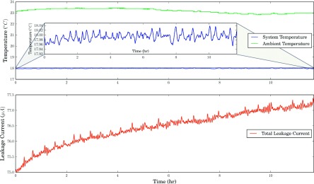
The average system temperature as well as the ambient temperature is shown in the top figure. The inset shows a zoomed version of the system temperature, showing that the temperature is stable within ±0.04 °C. The leakage current over the same time period is shown in the bottom figure. The current increases 1.28 μA between t = 0 h and t = 2 h. Between t = 2 h and t = 12 h, the current shows a linear slope of 0.13 μA h−1. Current shows a local oscillation, T = 10 min, with a maximum deviation of 0.3%.
FIG. 8.

Due to cooling from the edge of the imaging head, the PSAPDs experience different local fluctuations in temperature, as observed by variations in leakage current. These fluctuations were calculated for an average PSAPD closest to and furthest from the Peltier coolers. The FWHM is 0.79 and 2.34 nA for the center and edge PSAPDs, respectively. In this test, each PSAPD has an average current of 308.8 nA.
In another run of the system, the gain, as well as energy resolution, was measured from the PSAPDs over a period of 8.66 h. The total system energy resolution measured over the course of this measurement was 11.3% ± 0.1% FWHM at 511 keV. The resulting energy spectrum is shown in Fig. 9. The photopeak position, seen in Fig. 10, shows a maximum shift of 4 keV over this measurement. The photopeak shift was monitored in the same manner at three points separated by 2 day or more over the course of 10 day. Figure 10 shows that the system has a maximum photopeak position shift of 6 keV.
FIG. 9.

The energy spectrum measured from the system using data taken at eight time points over 8.66 h with 22Na source. The energy resolution was 11.3% ± 0.1% FWHM at 511 keV. The escape of a characteristic x-ray of Lu generates a shoulder that is clearly visible on the left side of the peak. This x-ray is typically absorbed in systems with larger crystal sizes so the escape peak cannot be seen. A fit of the sum of two Gaussians with a DC offset was used to extract the energy resolution at 511 keV. A more detailed discussion of the energy spectrum and fitting procedure can be found in Vandenbroucke et al. 2010. (Ref. 25).
FIG. 10.

On the top, the gain of the PSAPDs was measured every 75 min by integrating 1 × 10⁷ events over 15 min intervals. The average photopeak position for each PSAPD over all of the time points was identified and the average photopeak shift was then calculated for each time point. The first measurement was taken 72 min after system startup. On the bottom, the measurements were performed in the same manner at three points over the course of 10 days.
The control system was also tested on a successive run on its ability to handle a variety of changing conditions. The leakage current and temperature of the system from this experiment are plotted in Fig. 11. The system maintains a temperature of 18.00 ± 0.3 °C during these conditions.
FIG. 11.

Average fin temperature (top) is held to a tolerance of ±0.1°C during system operation through a variety of operating conditions, demonstrated by the total leakage current (bottom). The dashed line at “A” denotes when the reverse bias voltage to all of the PSAPDs is lowered 10 V. At “B” the reverse bias to one dual-PSAPD module is increased by 40 V. At “C” the reverse bias to all of the PSAPDs is brought down to zero.
4. DISCUSSION
The thermal regulation design demonstrates an ability to provide a stable environment for the PSAPDs to operate. The photopeak energy resolution of 11.3% ± 0.1%, seen in Fig. 9, measured over the course of 8.66 h shows that by using this thermal regulation system, a single energy window can be used without concern for count rate losses as has been observed and discussed in the literature.21,22 Furthermore, the thermal regulation system is able to provide well controlled temperature for the PSAPDs by keeping the system stable within ±0.05 °C, shown in Fig. 7. The cascaded PID loop method cooling method (Fig. 6) does show an increase in fluctuations of leakage current for the PSAPDs closest to the Peltier elements, compared to those in the center of the camera. However, the resulting FWHM, seen in Fig. 8, represents only 0.75% of each PSAPD’s average leakage current. This verifies that the use of thermal regulation from the edge of the imaging head does not detract significantly from the performance of the system.
In addition to providing stability to the system during data acquisition, the thermal regulation setup also had the goal of providing a constant operating environment in which calibration parameters for the system can be used. It can be seen from Fig. 10 that the gain is not as stable from run to run as it is while the system is operating (Fig. 10). However, the maximum photopeak shift of 6 keV represents a 1.12% shift in the photopeak. For an energy window twice as wide as the energy resolution, this shift would represent a 0.038% count loss from the photopeak while using the same calibration parameters. This sensitivity loss is acceptable, thus the system provides enough stability for calibration parameter and energy window reuse.
It is seen in Fig. 7 that there is an increase of leakage current over the course of the study. This also correlates with a gain increase that can be seen over time in Fig. 10. The upward shift in both gain and leakage current is consistent with a voltage increase or gain increase over the course of the study, and not a temperature drift. A shift in temperature would cause opposing responses in leakage current and gain when operating the PSAPDs at 18 °C and 1740 V.9 The voltage at the PSAPDs was measured in a repeated study to test whether heat from the backend electronics might cause shifts in the voltage supplied to the PSAPD, however, the voltage in this test was constant. After further discussion with the device manufacturers (Radiation Monitoring Devices, Inc.), it appears the PSAPDs have a period of warm-up time before their gain stabilizes. The shift is significantly longer than any expected scan time, so the effect on image quality from the shift is expected to be negligible. For longer scans where the gain can no longer be approximated as constant, the behavior has been reproduced consistently on independent multihour runs of the system. The gain stabilization time can also be mitigated by keeping the PSAPDs biased at a moderate voltage (1000 to 1200 V). We expect that this behavior can either be mitigated effectively, or modeled and calibrated out of the resulting data, so we expect little degradation of image quality from this effect.
5. CONCLUSION
We present a method of thermally regulating densely packed silicon photodetectors, including monitoring circuitry for their leakage current and temperature, as well as a control scheme for maintaining a consistent operating environment for these thermally sensitive detectors. We demonstrated these methods on a constructed prototype of a proposed high resolution PET camera, containing 256 PSAPDs in each of the two heads. Through the use of the feedback control loops, the temperature measured at the center of the rows of the PSAPDs was held to 18.00 ± 0.05 °C while the ambient temperature fluctuated over a range of 1.22 °C, from 22.22 to 23.44 °C, over a period of 13.66 h. This feedback control additionally held the maximum photopeak fluctuation of the PSAPDs below 4 keV during a 8.66 h period, demonstrating the functionality of the proposed regulation and control design. Measurements across multiple days show a maximum photopeak shift of 6 keV, validating that the thermal regulation system is able to stabilize operating conditions and allow calibration parameters to be reused for faster LOR acquisition. In addition to stability at specific operating points, the system shows robustness to changing operating conditions such as sudden voltage changes and module failure. This robustness reduces the need for operator intervention.
ACKNOWLEDGMENTS
The authors would like to thank Richard Farrell and Mickel McClish of RMD, Inc. for their help and the useful discussions. This work is supported in part by NIH-NCI Grant No. R01CA119056, DOD Grant No. W81XWH-10-1-03-93. D. L. Freese and D. F. C. Hsu are supported by a Stanford Graduate Fellowship. D. Freese also is supported by a National Science Foundation Fellowship.
REFERENCES
- 1.Yeom J. Y., Vinke R., and Levin C. S., “Optimizing timing performance of silicon photomultiplier-based scintillation detectors,” Phys. Med. Biol. 58, 1207–1220 (2013). 10.1088/0031-9155/58/4/1207 [DOI] [PMC free article] [PubMed] [Google Scholar]
- 2.Pichler B. J., Judenhofer M. S., Catana C., Walton J. H., Kneilling M., Nutt R. E., Siegel S. B., Claussen C. D., and Cherry S. R., “Performance test of an LSO-APD detector in a 7-T MRI scanner for simultaneous PET/MRI,” J. Nucl. Med. 47, 639–647 (2006). [PubMed] [Google Scholar]
- 3.Buzhan P., Dolgoshein B., Filatov L., Ilyin A., Kantzerov V., Kaplin V., Karakash A., Kayumov F., Klemin S., Popova E., and Smirnov S., “Silicon photomultiplier and its possible applications,” Nucl. Instrum. Methods Phys. Res., Sect. A 504, 48–52 (2003). 10.1016/S0168-9002(03)00749-6 [DOI] [Google Scholar]
- 4.Pichler B., Lorenz E., Mirzoyan R., Pimpl W., Roder F., Schwaiger M., and Ziegler S. I., “Performance test of a lso-apd pet module in a 9.4 tesla magnet,” in IEEE Nuclear Science Symposium (IEEE, Albuquerque, NM, 1997), Vol. 2, pp. 1237–1239. [Google Scholar]
- 5.Hawkes R., Lucas A., Stevick J., Llosa G., Marcatili S., Piemonte C., Del Guerra A., and Carpenter T. A., “Silicon photomultiplier performance tests in magnetic resonance pulsed fields,” in IEEE Nuclear Science Symposium Conference Record (IEEE, Honolulu, HI, 2007), Vol. 5, pp. 3400–3403. [Google Scholar]
- 6.Degenhardt C., Prescher G., Frach T., Thon A., de Gruyter R., Schmitz A., and Ballizany R., “The digital silicon photomultiplier—A novel sensor for the detection of scintillation light,” in IEEE Nuclear Science Symposium Conference Record (NSS/MIC) (IEEE, Orlando, FL, 2009), pp. 2383–2386. [Google Scholar]
- 7.Shah K. S., Farrell R., Grazioso R., Harmon E. S., and Karplus E., “Position-sensitive avalanche photodiodes for gamma-ray imaging,” IEEE Trans. Nucl. Sci. 49, 1687–1692 (2002). 10.1109/TNS.2002.801510 [DOI] [Google Scholar]
- 8.McClish M., Dokhale P., Christian J., Stapels C., Johnson E., Robertson R., and Shah K. S., “Performance measurements of CMOS position sensitive solid-state photomultipliers,” IEEE Trans. Nucl. Sci. 57, 2280–2286 (2010). 10.1109/TNS.2010.2050072 [DOI] [Google Scholar]
- 9.Vandenbroucke A., McLaughlin T. J., and Levin C. S., “Influence of temperature and bias voltage on the performance of a high resolution pet detector built with position sensitive avalanche photodiodes,” J. Instrum. 7, P08001 (2012). 10.1088/1748-0221/7/08/P08001 [DOI] [Google Scholar]
- 10.Roncali E. and Cherry S., “Application of silicon photomultipliers to positron emission tomography,” Ann. Biomed. Eng. 39, 1358–1377 (2011). 10.1007/s10439-011-0266-9 [DOI] [PMC free article] [PubMed] [Google Scholar]
- 11.Mars P., “Temperature dependence of avalanche breakdown voltage temperature dependence of avalanche breakdown voltage in p–n junctions,” Int. J. Electron. 32, 23–37 (1972). 10.1080/00207217208938266 [DOI] [Google Scholar]
- 12.Spanoudaki V. C., McElroy D. P., Torres-Espallardo I., and Ziegler S. I., “Effect of temperature on the performance of proportional APD-based modules for gamma ray detection in positron emission tomography,” IEEE Trans. Nucl. Sci. 55, 469–480 (2008). 10.1109/TNS.2007.912877 [DOI] [Google Scholar]
- 13.Petasecca M., Alpat B., Ambrosi G., Azzarello P., Battiston R., Ionica M., Papi A., Pignatel G. U., and Haino S., “Thermal and electrical characterization of silicon photomultiplier,” IEEE Trans. Nucl. Sci. 55, 1686–1690 (2008). 10.1109/TNS.2008.922220 [DOI] [Google Scholar]
- 14.Kataoka J., Sato R., Ikagawa T., Kotoku J., Kuramoto Y., Tsubuku Y., Saito T., Yatsu Y., Kawai N., Ishikawa Y., and Kawabata N., “An active gain-control system for avalanche photo-diodes under moderate temperature variations,” Nucl. Instrum. Methods Phys. Res., Sect. A 564, 300–307 (2006). 10.1016/j.nima.2006.03.033 [DOI] [Google Scholar]
- 15.Yamamoto S., Satomi J., Watabe T., Watabe H., Kanai Y., Imaizumi M., Shimosegawa E., and Hatazawa J., “A temperature-dependent gain control system for improving the stability of Si-PM-based PET systems,” Phys. Med. Biol. 56, 2873–2882 (2011). 10.1088/0031-9155/56/9/015 [DOI] [PubMed] [Google Scholar]
- 16.Kaplan A., “Correction of SiPM temperature dependencies,” Nucl. Instrum. Methods Phys. Res., Sect. A 610, 114–117 (2009). 10.1016/j.nima.2009.05.137 [DOI] [Google Scholar]
- 17.Raylman R. R., Stolin A., Majewski S., and Proffitt J., “A large area, silicon photomultiplier-based PET detector module,” Nucl. Instrum. Methods Phys. Res., Sect. A 735, 602–609 (2014). 10.1016/j.nima.2013.10.008 [DOI] [PMC free article] [PubMed] [Google Scholar]
- 18.Hughes P. J., Herbert D., Stewart A., and Jackson J. C., “Tiled silicon photomultipliers for large-area low-light sensing applications,” Proc. SPIE 6471, 647112-1–647112-8 (2007). 10.1117/12.700900 [DOI] [Google Scholar]
- 19.Du J., Schmall J. P., Yang Y., Di K., Dokhale P. A., Shah K. S., and Cherry S. R., “A simple capacitive charge-division readout for position-sensitive solid-state photomultiplier arrays,” IEEE Trans. Nucl. Sci. 60, 3188–3197 (2013). 10.1109/TNS.2013.2275012 [DOI] [PMC free article] [PubMed] [Google Scholar]
- 20.Lau F. W. Y., Vandenbroucke A., Reynolds P. D., Olcott P. D., Horowitz M. A., and Levin C. S., “Analog signal multiplexing for PSAPD-based PET detectors: Simulation and experimental validation,” Phys. Med. Biol. 55, 7149–7174 (2010). 10.1088/0031-9155/55/23/001 [DOI] [PMC free article] [PubMed] [Google Scholar]
- 21.Keereman V., Van Holen R., Vandenberghe S., and Vanhove C., “Temperature dependence of APD-based PET scanners,” Med. Phys. 40, 092506 (13pp.) (2013). 10.1118/1.4819823 [DOI] [PubMed] [Google Scholar]
- 22.Cadorette J., Bergeron M., Thibaudeau C., Beaudoin J.-F., Pepin C. M., and Lecomte R., “Comment on ‘Temperature dependence of APD-based PET scanners’ [Med. Phys. 40(9), 092506 (13pp.) (2013)],” Med. Phys. 41, 017101 (1pp.) (2014). 10.1118/1.4856097 [DOI] [PubMed] [Google Scholar]
- 23.Lau F. W. Y., Fang C., Reynolds P. D., Olcott P. D., Vandenbroucke A., Spanoudaki V. C., Olutade F., Horowitz M. A., and Levin C., “1 mm3 resolution breast-dedicated pet system,” IEEE Nuclear Science Symposium Conference Record (IEEE, Dresden, Germany, 2008), pp. 5619–5622. [Google Scholar]
- 24.Zhang J., Foudray A. M. K., Olcott P. D., and Levin C. S., “Performance characterization of a novel thin position-sensitive avalanche photodiode for high resolution positron emission tomography,” IEEE Trans. Nucl. Sci. 54, 415–421 (2007). 10.1109/TNS.2007.894128 [DOI] [Google Scholar]
- 25.Vandenbroucke A., Foudray A. M. K., Olcott P. D., and Levin C. S., “Performance characterization of a new high resolution PET scintillation detector,” Phys. Med. Biol. 55, 5895–5911 (2010). 10.1088/0031-9155/55/19/018 [DOI] [PMC free article] [PubMed] [Google Scholar]
- 26.Zhai J., Vandenbroucke A., and Levin C. S., “Thermal regulation for apds in a 1 mm 3 resolution clinical pet camera: Design, simulation and experimental verification,” Phys. Med. Biol. 59, 3951–3967 (2014). 10.1088/0031-9155/59/14/3951 [DOI] [PubMed] [Google Scholar]
- 27.Vandenbroucke A., Innes D., and Levin C. S., “Effects of external shielding on the performance of a 1mm3 resolution breast PET camera,” IEEE Nuclear Science Symposium Conference Record (NSS/MIC) (IEEE, Knoxville, TN, 2010), pp. 3644–3648. [Google Scholar]
- 28.Nolas G. S., Thermoelectrics : Basic Principles and New Materials Developments (Springer, Berlin, 2001). [Google Scholar]
- 29.Lau F. W. Y., “Design and development of a 1 mm resolution clinical positron emission tomography (PET) system,” Ph.D. thesis, Stanford University, 2013. [Google Scholar]
- 30.iseg Spezialelektronik GmbH, EHS Standard HV Modules 8 Channels with Common-GND Operator’s Manual, 20140115th ed. (iseg Spezialelektronik GmbH, Rossendorf, Germany, 2014). [Google Scholar]