

Abstract
Previous measurements of the electronic conductance of DNA nucleotides or amino acids have used tunnel junctions in which the gap is mechanically adjusted, such as scanning tunneling microscopes or mechanically controllable break junctions. Fixed-junction devices have, at best, detected the passage of whole DNA molecules without yielding chemical information. Here, we report on a layered tunnel junction in which the tunnel gap is defined by a dielectric layer, deposited by atomic layer deposition. Reactive ion etching is used to drill a hole through the layers so that the tunnel junction can be exposed to molecules in solution. When the metal electrodes are functionalized with recognition molecules that capture DNA nucleotides via hydrogen bonds, the identities of the individual nucleotides are revealed by characteristic features of the fluctuating tunnel current associated with single-molecule binding events.
Keywords: recognition tunneling, DNA sequencing, tunnel junction, chemical recognition
Much of the human genome consists of repeated sequences, and these are difficult to assemble with the short reads of current next-generation sequencing. Nanopore sequencing offers the possibility of very long reads of DNA with single molecule sensitivity.1 In the current version of nanopore sequencing, the sequence is sensed via the changes in the degree to which ion current is blocked as a polymer translocates through the pore. This current blocking is sensitive to several nucleotides, so many different current levels must be sensed and assigned to blocks of nucleotides, with the result that the sequence reads are prone to errors,2 though substantial data can be recovered with improved pores.3 To overcome this limitation, Zwolak and DiVentra proposed sensing DNA nucleotides via measurements of transverse tunnel current as a DNA molecule is passed through a gap between two electrodes.4 Attempts to make solid-state, fixed gap tunnel junctions for reading DNA ncleotides are described by Fischbein et al.,5 Healy et al.,6 Spinney et al.,7 Ivanov et al.(8,9) Redenovic et al.(10) and Liang and Chou.11 In the best cases, these papers report the detection of whole DNA molecules as single events with no chemical information. Two groups have reported tunnel detection of the DNA nucleotides, but only with adjustable tunnel gaps. In one case, the metal electrodes of a scanning tunneling microscope (STM) were functionalized with molecules that are strongly bonded to the electrodes and form weak hydrogen bonds with the DNA nucleotides (a process called “recognition tunneling”, RT). RT can detect and separate all four DNA nucleotides and 5-methyl cytosine12 as well as a number of amino acids and peptides13 using a fairly large gap (∼2 nm14). In another approach, a mechanically controllable break junction (MCB) is used to create fresh metal surfaces in solution. When a very small gap (0.5 to 0.8 nm) is used, both DNA nucleotides15,16 and amino acids17 are detected. Neither the STM nor MCB approaches are scalable, nor are they compatible with incorporation of a nanopore. The development of a solid state tunneling device that is sensitive to all five nucleotides and compatible with the incorporation of a nanopore is described in this paper.
Electrode gaps for sequencing DNA have been made by cutting gold5,6 or carbon7 nanowires with an electron beam, by using electromigration16 or mechanical stress18 to break a gold wire, or electron-beam induced deposition of opposed pairs of wires.9,19 An alternative approach is to use a layered structure to define the size of a gap, allowing molecules to bond between electrodes exposed at the edges of the device. These multilayer edge molecular electronic devices (MEMED) have been reviewed by Tyagi.20 We have coupled this layered structure with RT to make a device that is sensitive to molecules dissolved in solution in contact with the device. In addition to its potential scalability and compatibility with a nanopore, the device described here overcomes several limitations of the STM: (1) The servo system used to maintain the gap distorts RT signals by pulling the probe away from the surface as the current rises.12 (2) The contact point (and thus the gap size) is difficult to determine.14 (3) It is difficult to maintain a constant gap size as the bias is changed, and impossible when the current has a nonlinear dependence on bias. (4) Constant currents arising from molecular adsorption may be compensated for by the STM current servo, and so are not observable. The fixed-gap device described here overcomes these problems, yielding data that give new insights into the physics and electrochemistry of the RT process.
Experimental Approach
Size of the Tunnel Gap
Given the uncertainties in measurement of STM gap sizes, we made tunnel junctions using electron-beam cuts in nanowires suspended on thin membranes (Supporting Information, Figure S1a) so that the gap size could be measured directly (Figure S1b) in a transmission electron microscope (TEM). We found that gaps between 1.8 and 2 nm gave RT signals (data summarized in Figure S2). This is a little smaller than the 2.5 nm estimated from break junction measurements,14 but subject to much less uncertainty. Thus, 2 nm was chosen as our target size for a fixed tunnel gap.
Fabrication of Layered Junctions
Layered tunnel junctions were made by first defining a 10 nm thick Pd electrode on a Si wafer using e-beam evaporation and liftoff (the lower electrode in Figure 1a). One nanometer of Ti was used as an adhesion layer to bond to the native oxide and the Pd electrode was contacted by gold electrodes (labeled A1 and A2 in the top-down SEM image shown in Figure 1b). Plasma-enhanced atomic layer deposition (PEALD) was used to grow a ∼2 nm thick layer of Al2O3 (gray layer in Figure 1a). A 50 nm wide Pd nanowire wire (10 nm Pd, 1 nm Ti) was deposited on top of the Al2O3 dielectric using e-beam lithography (EBL). This wire is shown connected to gold electrodes B1 and B2 in Figure 1b. We used a nanowire because wires below 100 nm in width almost always yielded nonshorted devices. These devices gave tunnel currents (Figure 1e, Supporting Information, Figures S3 and S4) consistent with the Simmons formula21 though departures from ideality at high bias suggest that defects and/or electrochemical effects play a role. A tunnel current that scaled with the junction area was an important hallmark of successful fabrication. Figures S3 and S4 show (a) quantitative agreement with the Simmons model given the measured junction properties as input and (b) the fact that after making cuts through the junction, the tunnel current density (determined from measured junction area) was unchanged.
Figure 1.

Fabrication of layered tunnel junctions. (a) (i) 10 nm thick Pd electrode is defined on a silicon support; (ii) 2 nm thick Al2O3 layer is deposited by ALD; (iii) second 10 nm thick Pd nanowire is deposited on top of the dielectric layer; (iv) a hole cut into the sandwich (“RIE Cut”) exposes the junction giving access to analyte molecules (red dots). (b) SEM image of the top view of a device before cutting. The lower Pd electrode is contacted by gold electrodes A1 and A2. The top 50 nm-wide Pd nanowire is contacted by electrodes B1 and B2 (the Al2O3 layer is not visible). (c) SEM image of the center of the device after a hole was cut by RIE. (d) TEM image taken through a thin section lifted out of the junction region by FIB. The bulk of the dielectric layer is about 3 nm in thickness, narrowing to 2 nm at the RIE cut (red arrow). (e) Tunnel current vs bias before (blue) and after (red) the RIE cut. The current falls in proportion to the reduction in junction area after cutting (Supporting Information, Figure S3).
The next step was to cut through the electrodes to expose the gap to analyte solutions (Figure 1a,c), and this proved to be challenging. Electron beams, Ga-focused ion beams, and argon ion sputtering all caused the metal electrodes to melt or move, shorting devices completely in most cases. Selective reactive ion etching (RIE, see Methods) proved quite effective, with a yield of about 30% for devices with undamaged junctions. The test criterion was that the cut junction gave a reduced tunnel current after cutting, consistent with the reduction in junction area (Figure 1e and Supporting Information, Figure S3).
TEM imaging of the cross-section of working junctions (Figure 1d) showed that the ALD was thicker than the target 2 nm, but this was compensated for by some degree of closing of the electrode gap after cutting, resulting in the desired 2 nm gap in about 30% of the junctions.
Sample Interface
A 1 μm thick PMMA mask was used to define the area etched by RIE. This mask was also used as a passivation layer and bonding surface over which a microfluidic cover was mounted (Figure 2a). The final device was immersed in an ethanolic solution of the recognition-molecules (4(5)-(2-mercaptoethyl)-1H-imidazole-2-carboxamide, ICA) overnight (∼20 h). After rinsing and drying, the polydimethylsilxoane (PDMS) microfluidic cover was pressed onto the chip (Figure 2a). Fluid lines were used to draw solutions through the microfluidic channel using a syringe. The device was mounted on a probe station inside a Faraday cage and an Ag/AgCl reference electrode was held at constant bias relative to the bottom electrode (Figure 2b). Bias was applied across the gap and tunnel current was recorded using an Axon Axopatch 200B (Molecular Devices). Control experiments were carried out (1) using phosphate buffer solutions alone, (2) using analyte solutions with unfunctionalized devices, and (3) using functionalized electrodes with phosphate buffer solutions. The featureless current trace in Figure 2c is representative of the results from these three types of experiment. Both analyte molecules and functionalized electrodes were required to produce RT signals, and Figure 2d shows the signal given by the device that gave no signals (Figure 2c) in the three control experiments. These controls have been reproduced many times with consistent results in devices with gaps from 1.8 to 2 nm.
Figure 2.

Fluid interface: (a) Optical image looking through the PDMS microfluidic on top of the device. The arrow shows the direction of fluid flow. (b) Biasing of the junction. The lower electrode is held at a potential Vref with respect to an Ag/AgCl reference electrode. The top electrode is held at Vbias with respect to the lower electrode. Tunnel current is measured with a transconductance amplifier I. Red dots symbolize two molecules trapped by the recognition molecules tethered to the electrode surfaces. (c) Control experiments with the electrodes unfunctionalized, or functionalized with no analyte present, or unfunctionalized with no analyte present produce no signals. (d) When the same device is functionalized and an analyte present (100 μM dGMP) the current jumps up to a large constant value with superimposed current fluctuations. The inset shows how this signal is largely abolished by rinsing the device. (e) In the absence of a reference electrode devices show large swings in current with slow transitions between states. These instabilities vanish when the device is connected to a reference electrode (f).
It proved essential to couple one of the electrodes to a reference electrode in contact with the analyte solution (Figure 2b) so that both electrodes (one at Vref, the other at Vref + Vbias) were held in the double layer range of potential with no significant Faradaic processes at either electrode22 (but see the following). Vref was typically + 100 mV vs Ag/AgCl with a maximum value of 400 mV used for Vbias. Currents in this system are small, and, in contrast to macroscopic electrochemistry, the positioning of the reference electrode was not critical, so it was placed upstream of the microfluidic cover for simplicity. The devices showed violent current swings in the absence of a reference (Figure 2e) and stabilized as soon as a reference was connected (Figure 2f).
Results and Discussion
Chemical Sensing
Examples of chemically sensitive signals are given in Figure 3a. This shows the tunnel current as 100 μM solutions of the four naturally occurring DNA nucleoside 5′-monophosphates (dAMP, dCMP, dGMP, and dTMP) were flowed through a device (Vbias = +400 mV) one after another, and rinsed with buffer in between to remove bound molecules. The signals consist of two components: current spikes that vary in amplitude from tens to hundreds of pA, depending on the analyte, and a steady baseline current (BL) of between tens and hundreds of pA, again with a magnitude that depends on the analyte. Neither signal (baseline or spikes) was present in buffer alone (“Rinse” in Figure 3a) showing that the baseline and current spikes were generated by DNA nucleotides. Both the magnitude of the baseline signal and the character and frequency of the spikes are strongly dependent on the concentration of analyte, as shown in Figure 3. In particular, the magnitude of the baseline signal changes with analyte concentration in a manner that is well-fitted by a Langmuir–Hill adsorption isotherm (Figure 3b). The current spikes at 100 μM concentration are reminiscent of STM signals obtained at similar concentration12,13 but the baseline is a new feature. The baseline signal was not present in the nanowire junctions used to determine the optimal gap (Supporting Information, Figure S2) suggesting that it is a consequence of the larger junction area in the layered junctions. STM junctions are also small laterally and so would not show this feature: Assuming that this current is proportional to the exposed junction area, the largest baseline current (of about 400 pA in this 50 nm wide junction) would be reduced to <8 pA in an STM junction (which is less than 1 nm in extent). Furthermore, a small steady baseline current would be compensated for by the STM servo and so remain undetected even if it were present in an STM experiment.
Figure 3.

Representative signals and their concentration dependence. (a) Current vs time for device 1 as ∼100 μM solutions of nucleotides in 1 mM phosphate buffer (pH ≈ 7.0) were passed through the device. Rinses in-between (black) used phosphate buffer. Noise associated with the beginning and end of flush cycles has been omitted for clarity except in the region circled in red. The signals consist of current spikes on top of a baseline current (“BL”) that changes with analyte and disappears when the device is rinsed. (b) The baseline signal increases with concentration of dAMP consistent with a Langmuir–Hill adsorption isotherm (solid line for KH = 0.7 μM). (c,d,e) Sample traces from three different devices at 100 μM (c), 1 μM (d), and 10 nM (e) dAMP in 1 mM phosphate buffer. Blowup in panel e shows 5 to 10 pA steps (“SF”) in the baseline current. The less-frequent large signal spikes are labeled “LF”. This concentration dependence is confirmed by a series of measurements at different concentrations of dAMP in one device: panel f shows distributions of LF amplitudes (baseline subtracted). Signal traces in panels c and d were filtered (see Methods).
In contrast to the STM, which required a sample with micromolar concentration, these fixed-gap devices gave clear signals with nanomolar concentrations of analyte. Figure 3 panels c, d, and e show how the signal changes from a relatively pattern-less signal at 100 μM, to switching between a series of current plateaus (ΔI, Figure 3d) at 1 μM, to individual signal pulses (labeled “LF” for large fluctuations) on a background of small fluctuations (labeled “SF”) at 10 nM (Figure 3e). These experiments were performed on three different devices, so we verified these trends by measuring the changes in current distributions on one device as concentration was increased from 10 nM to 1 mM (Figure 3f). The amplitude distribution (relative to the baseline, “BL”) changed from a single sharp peak to a much broader, higher amplitude distribution as the analyte concentration was increased.
Device-to-device variations are significant23 and were characterized using six different devices. Signal amplitudes changed considerably, but the order of the amplitudes, and their frequency characteristics, varied in a consistent way with each of the four nucleotides (Supporting Information, Figure S5, 100 μM; Figures S6, S7, 1 μM).
Chemical sensitivity and reproducibility in the nanomolar concentration range are illustrated in Figure 4. The existence of sharply defined current levels and the exponential distribution of arrival times between signal spikes at nanomolar concentrations (Figure 5) suggest a Poisson process in which the individual binding events are being resolved. Figure 4a shows amplitude histograms for yet another device for dAMP, dGMP, and dCMP (dTMP is difficult to flush from the system, complicating repeat measurements). These distributions show absolute values of current, and are the sum of contributions from the chemically sensitive baseline, small fluctuations (SF), and large fluctuations (LF) so the distributions are quite complicated. Nonetheless, when measurements were repeated on the same device (dashed lines in Figure 4a) the distributions were reproduced quite well. Similar repeated measurements are shown for other devices in Supporting Information, Figure S8.
Figure 4.

Signal features at low concentrations. (a) Current amplitude distributions for three nucleotides measured over two repeated runs (device 5) at 10 nM analyte concentration. (b) Distributions of the amplitudes of the large fluctuations (LF). (c) Distributions of the values of the current step between plateaus for the small fluctuations (SF) for dAMP (red), dGMP (blue), dCMP (green), dTMP (orange), and 5Me-dCMP (purple). (d) Distributions of the width of the current plateaus for the SF. Solid lines are fits using the sum of two exponentials and the decay times are listed in Table 1. (e) Scatter plot of plateau widths vs current step values for all five nucleotides. (f) Data for dAMP, dGMP, and dCMP (replotted from panel e) with similar data for two other devices at 10 nM (g) and 1 nM (h). All devices were operated at Vbias = 0.38 V and Vref = 0.1 V.
Figure 5.
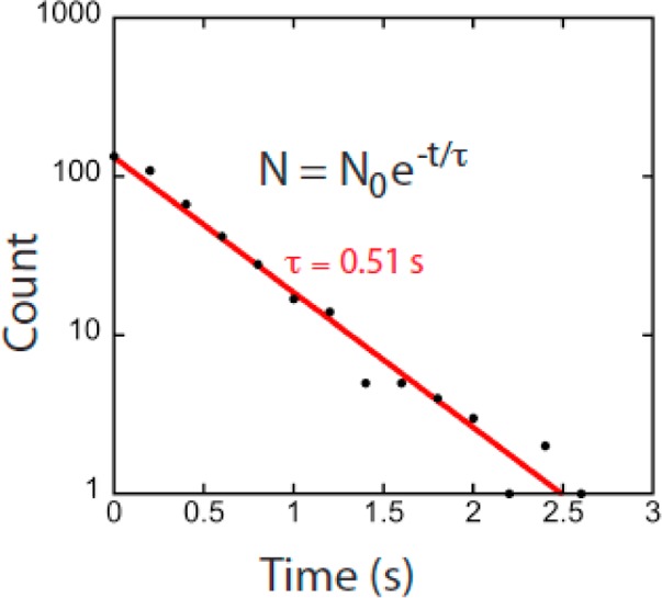
At 10 nM dAMP, the intervals between the large signal spikes (“LF” Figure 3e) are distributed as a single exponential, consistent with single-molecule events.
Better insight into the chemical sensitivity of the devices comes from analyzing the large (LF) and small (SF) fluctuations separately. Figure 4b shows the LF distributions, obtained by measuring the height of the larger peaks relative to the baseline value immediately preceding the onset of the peak. Similar data for other devices is shown in Supporting Information, Figure S9. Both the shape and order of the distributions change from device to device.
The small fluctuations (SF) were analyzed by determining the current steps between levels located in the baseline. These levels are clear without any filtering in the trace shown in Figure 3e, but were often obscured by noise in other runs. In these noisier traces, the SF were revealed after Hidden-Markov Random Field filtering (see Methods). Distributions of the step values are quite sharp, though the distributions for dCMP and 5Me-dCMP overlap (Figure 4c). The duration of the SF current plateaus also varies with analyte (Figure 4d and Table 1). The combined use of multiple signal features enhances separation of single-molecule data.13,24 This is illustrated in Figure 4e which shows how the combined use of plateau widths and current step heights resolves many of the reads for all five nucleotides. Reads of dAMP, dGMP, and dCMP were repeated on two other devices at 10 nM and 1 nM concentrations and scatter plots of plateau width vs current step are similar in overall appearance, though absolute current values are different (Figure 4f–h).
Table 1. Current Plateau Duration Times Fitted to a exp (−(t/τ1)) + b exp(−(t/τ2)).
| nucleotide | τ1 (ms) | τ2 (ms) |
|---|---|---|
| dAMP | 28.6 ± 3 | 163 ± 60 |
| dGMP | 7.4 ± 0.3 | 74 ± 4 |
| dCMP | 27.3 ± 5 | 189 ± 140 |
| dTMP | 5.7 ± −0.4 | 67 ± 4 |
| 5Me-dCMP | 5.7 ± 0.4 | 89.2 ± 6 |
The trends in terms of relative signal size for each nucleotide are different for the SF and LF. We propose (discussion of Figure 7 below) that there are two different types of binding responsible for the two types of fluctuation. If this is indeed the case, it would account for the different order of amplitudes as a function of nucleotide for the two types of fluctuation.
Figure 7.
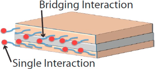
Two types of interaction that might account for the two types (LF and SF) of fluctuation observed.
Thus, it is clear that any one device can resolve different analytes well, but there is also considerable device-to-device variation, probably requiring the use of calibration samples to make the technology robust.
Voltage Dependence of RT Signals
The fixed tunnel gap allows the voltage dependence of the signals to be investigated without the complications of the STM current servo changing the gap. STM data25 hint at a nonlinear current–voltage characteristic, but it is immediately obvious in the fixed-gap device. Figure 6a shows current recordings as a function of bias with a 10 nM dAMP solution (a similar series of recordings are shown for another device in Supporting Information, Figure S10). The amplitudes of both the baseline (BL) and the large fluctuations (LF) increase significantly above about 300 mV bias. Figure 6b and Supporting Information, Figure S10b show that the conductance of the device increases significantly when the bias exceeds ∼350 mV. This effect is not seen in experiments with the phosphate buffer alone (“Control” in the figures). One explanation for a change in molecular conductance is the reduction or oxidation of a neutral species.26 Cyclic voltammetry (Figures 6c,d and Supporting Information, Figure S11) shows evidence of a reversible oxidation of the ICA monolayer at about 400 mV vs Ag/AgCl. The feature is abolished by a slight reduction in pH, suggesting that it is caused by a deprotonation of the ICA (Figure S11g). Figure 6d shows the excess of electrochemical current over bare Pd for an ICA monolayer (black line, buffer only) and in the presence of 100 μM of each of the nucleotides. Since the effect is not changed by adding the nucleotides, we conclude that the increased conductance originates with the ICA molecules. In the tunneling devices, the bottom electrode (Figure 2b) is held at +100 mV vs Ag/AgCl, so the top electrode is at +450 mV vs Ag/AgCl when the conductance increases, close to value for peak currents in the macroscopic electrochemical measurements (Figure 6d). Thus, the increased conductance at high bias is consistent with deprotonation of the ICA at potentials above about +400 mV vs Ag/AgCl.
Figure 6.

Nonlinear current–voltage characteristics. (a) Current traces as the device bias was stepped from 0.4 V down to 0.26 V with the bottom electrode at +100 mV with respect to the Ag/AgCl reference. Data are for device 4 with 10 nM dAMP. The response is reversible as shown by a return to 0.38 V (blue trace). (b) Plot of LF amplitudes (blue) and baseline current (BL) vs bias for the data shown in panel a. Data for control runs (buffer only) are given in purple and green. (c) Cyclic voltammetry for an ICA-covered Pd surface in 1 mM phosphate buffer. Each curve corresponds to the upper sweep voltage listed. Similar measurements (inset) for a bare Pd surface do not show the excess currents at the turn-around points (circled in red) observed when the surface is functionalized with ICA. (d) Plot of the excess current at the turn-around point for the ICA-functionalized Pd (black) and also in the presence of each of the four nucleotides, showing that the excess current is due to the ICA, and not nucleotides.
Baseline Current
The baseline signal is clearly generated by binding of analyte molecules to the ICA recognition molecules. It changes with analyte (Figure 3a) and increases with sample concentration (Figure 3b). The current path must be through the ICA molecules because the baseline signal also changes on oxidation of the ICA (Figure 6b and Supporting Information, Figure S10). A plausible model for this behavior is proposed in Figure 7. Binding events at just one ICA molecule (“Single Interaction” in the figure) could cause increases in current by, for example, changing the polarization of the medium near the gap. These should be relatively frequent events (because alignment is not so critical for binding) and give smaller current steps (because the gap is not bridged). Binding events that couple two ICA molecules across the gap (“Bridging Interaction” in the figure) would give rise to larger signals (LF) and be less frequent because reader molecules would have to be positioned appropriately on both electrodes.
Conclusions
We have presented a potentially scalable process for manufacturing tunnel junctions with a 2 nm gap into which analyte solutions can be flowed, and we have demonstrated single nucleotide identification using these devices. Functionalized with recognition molecules, the junctions produce signals that change with the DNA nucleotide in solution. Devices operate reliably for many hours (and can often be repaired by refunctionalizing them). At high concentrations, the signals are complicated by the overlap of many single molecule contributions. Features associated with single molecule binding events dominate at low concentrations. At present, devices are completed one at a time, limiting our ability to gather a large body of statistics on different analytes, so it is not yet clear that all four DNA nucleotides and their epigenetic modifications will be resolved on every device. That said, the following signal features are robust from device to device: (a) Introduction of an analyte molecule generates a constant background current that depends on the analyte and increases with increasing concentration of analyte. (b) Sitting on top of this background current are signal spikes that are different in character for each analyte. The relative height of these spikes is consistent from device to device. However, both the magnitude of the spikes and the magnitude of the background current vary significantly from one device to another. We are developing wafer-scale processes to increase both the production and uniformity of devices at which point we will be able to better characterize these variations.
The development of sequencing on these chips will require the inclusion of a nanopore or planar nanochannel to translocate polymer chains past the tunnel gap. This may be accomplished using RIE to cut through both the junction and the underlying substrates (by which means nanopores as small as 20 nm in diameter have been mass-produced27).
Even without a nanopore, the devices yield useful insights into the electronic and electrochemical properties of single molecules. They operate down to a nanomolar concentration region, as low as the best that can be done with mass spectrometry and better than next generation sequencing (which requires PCR or rolling circle amplification). The ability to detect single binding events electronically may pave the way for applications beyond biomolecular sequencing. For example, electrodes could be functionalized with specific cognate ligands that recognize rare proteins in solution, a label-free, electronic equivalent of an ELISA assay.
Methods
Fabrication of Nanowire Junctions on TEM Membranes
Devices with coplanar Pd electrodes separated by a nanogap were created by milling Pd nanowires on 50 nm-thick SiN membranes using a focused, high-energy electron beam. These devices were fabricated by first coating a double-side polished ⟨100⟩ Si wafer with a 50 nm LPCVD SiN film. The SiN layer on the backside of the wafer was then patterned into a hard mask (HM) for subsequent TMAH etching, using photolithography followed by a reactive-ion etch to open 1 mm2 windows, completely removing the SiN in these regions. After defining the SiN HM, TMAH was used to anisotropically etch V-shaped wells completely through the 700 μm Si substrate, stopping on the frontside SiN layer, leaving a 50 nm-thick SiN membrane suspended over an 80 μm square window.
Following substrate preparation, leads with connecting probe pads and Pd nanowire electrodes were fabricated using a two-step lithography and liftoff approach. First, lead electrodes and pads were formed using photolithography, electron beam (e-beam) evaporation, and liftoff to form Ti/Pd (10 nm/50 nm) contacts. A second step involved e-beam lithography on a poly(methyl methacrylate) A2 (PMMA) resist with subsequent Ti/Pd (1 nm/9 nm) deposition and liftoff in hot acetone (80 °C) to define the Pd nanowires, which were aligned to the center of the membranes with fanout contacts to the lead pattern. The entire structure was then conformally coated with 5 to 7 nm Al2O3 to isolate the electrodes from solution during RT experiments. To do this, Al was sputter-coated in 1 nm increments and oxidized iteratively for a total of five times, a process adopted to minimize pinholes in the oxide. Finally, the wafer was diced into a chip size compatible with TEM, where nanogaps were formed by focusing a 300 kV e-beam across the Pd nanowire, only leaving exposed the Pd metal on the sidewalls of the nanogap. Devices were insulated with an Al2O3 and tunneling measurements carried out as described in the Supporting Information (Figures S1–S2 and accompanying text).
Fabrication of Layered Junctions
Au leads and pads were fabricated by photolithography or electron-beam lithography (EBL) with a JEOL JBX 6000FS/E, using either ⟨100⟩ polished Si wafers or on 5 mm chips containing 50 nm thick silicon nitride windows (purchased from Norcada, Alberta). Bottom electrodes were made from 6 μm wide wires by electron beam evaporation of Ti (1 nm)/Pd(10 nm) (Lesker PVD75). After ALD of the dielectric layer, Pd nanowires of 50 nm to ∼80 nm width made of Ti (1 nm)/Pd(10 nm) were fabricated by EBL using a 60 nm thick layer of poly(methyl methacrylate) (A2) spun over the entire chip surface. The nanowire patterns were exposed at a dose of 500 μC/cm2. The metal lift-off process was carried out by soaking the chip in dichloromethane for about 15 min, followed by the rinses with acetone, isopropyl alcohol (IPA), and DI water and finally blown dry using nitrogen gas.
Plasma-Enhanced Atomic Layer Deposited Al2O3 Films
The Al2O3 insulator layers were deposited by remote plasma-enhanced atomic layer deposition (PEALD) using dimethylaluminum isopropoxide (DMAI, [(CH3)2AlOCH(CH3)2]2) as the aluminum containing precursor.28 Samples were mounted onto a 1 in. round molybdenum sample holder, loaded into a ultrahigh vacuum (UHV) transfer line, and transferred into the PEALD chamber. In some cases the samples were cleaned using a remote hydrogen plasma process prior to PEALD growth. The custom PEALD system28 employs a remote oxygen plasma generated in a quartz tube ∼25 cm above the sample, and the precursors are delivered to the chamber using Ar as the carrier gas. The total time of a cycle is approximately 1 min with a 0.6 s precursor pulse, 20 s N2 purge, 6 s O2 purge, 8 s O2 plasma, and 20 s N2 purge. With these conditions the Al2O3 growth rate was ∼1.5 Å/cycle within the temperature window between 25 to 220 °C. The sample temperature was maintained at ∼180 °C during the deposition process. The films were targeted at thicknesses of 2.0 to 3.5 nm, requiring 13 to 23 deposition cycles.
RIE Cuts through the Junctions
A 3 μm × 6 μm window was fabricated over the tunnel junction using EBL with a 1.0 μm ∼ 1.5 μm thick PMMA layer. RIE was carried out using an Oxford Plasmalab 80plus. The top Pd nanowire was etched with Cl2 (gas flow rate: 8 sccm) and Ar (20 sccm), chamber pressure ∼10 mT, with a power of 250 W for 100–120 s. The Al2O3 was etched with BCl3 (40 sccm), at a chamber pressure of ∼15 mT and power of 200 W for 60 s. The Pd bottom electrode was etched with Cl2 as described above for 75–100 s.
FIB Lift-Out of a Cross Section of the Junction
A 1 μm Pt strip was deposited over the junction area using a Nova 200 Nanolab. The same FIB was used to mill trenches on each side of the strip, which was then pulled out using an Omniprobe holder. The sample was thinned to a final thickness of ∼100 nm and imaged using a JEOL 2010F. The Ga ions disrupt the surface layers, but these images are projections through the entire 100 nm thickness of the sample.
Cleaning and Functionalization with ICA
After RIE, the chips were rinsed with ethanol and blow-dried with N2 gas. They were then immersed in an ethanolic solution of 4(5)-(2-thioethyl)-1H-imidazole-2-carboxamide (0.5–2 mM) and left for a minimum of 20 h, rinsed with ethanol, and blow-dried with nitrogen. A PDMS microfluidic was pressed on to the top PMMA layer, and the device was mounted in a Faraday cage for measurement.
Solutions of DNA Nucleotides
2′-Deoxyadenosine 5′-monophosphate (dAMP, H form, catalog no.: d6375; Sigma grade, 98–100%), 2′-deoxycytidine 5′-monophosphate (dCMP, H form, catalog no.: D7750; Sigma grade, ≥95%), 2′-deoxyguanosine 5′-monophosphate (dGMP, sodium form, catalog no.: D9500; HPLC grade, ≥99%), and thymidine 5′-monophosphate (dTMP, disodium form, catalog no.: T7004; Sigma grade, ≥99%) and 5-methyl-2′-deoxycytidine-5′-monophosphate, (disodium salt, ≥98%, USB catalog no. 19184) were used as received. Stock solutions were prepared by dissolving nucleotides in phosphate buffer (1 mM, pH 7.5), and their concentrations were determined by means of UV spectroscopy. High concentrations of nucleotide resulted in a small reduction in pH (Supporting Information, Table S1).
Noise Filtering Algorithm
Long-time scale fluctuations in the baseline signal were removed by fitting the signal to a second-order polynomial; f(y(t),m,a) = y(t) – mt – at2 where y(t) is the signal value at time t and m and a are determined by minimizing the following cost function: J = (σw + σL + n)2 where σw is the standard deviation of the whole signal train, σL is the standard deviation of the plateau levels and n is the number of plateau levels. To carry out this calculation, we first located current plateaus using the Variational Baysean Gaussian Mixture Model, VBGMM.29 VBGMM was not good at classifying levels in the presence of slow baseline variations, so we used the Hidden Markov Random Field with Expectation Maximization (HMRF-EM)30 to extract levels from the filtered data. These levels were used to calculate the current steps between one current plateau and the next as well as the plateau durations (step widths shown in Figure 3).
Acknowledgments
We thank Brett Gyarfas, Nathan Newman, and Predrag Krstic for useful discussions. Ankit Goratela assisted with electrical measurements. Young Kwark produced instrumentation for measurements for the gapped device. Device fabrication was carried out in the NNIN facility in the Center for Solid State Electronics Research at ASU and at the Microelectronics Research Laboratories (MRL) at IBM T. J. Watson Research Center. TEM imaging and sample preparation were carried out in the John Cowley Center for High Resolution Electron Microscopy with the assistance of Jason Ng and at the MRL in IBM T. J. Watson Research Center. This work was funded by a grant from the NHGRI (HG006323) and was also funded from a sponsored research agreement from Hoffmann-LaRoche.
Supporting Information Available
Fabrication of nanowire junctions, RT signals from nanowire junctions, tunnel current characteristics of layered junctions, examples of chemically sensitive signals from various devices, further example of bias dependence, electrochemical data from model surfaces. This material is available free of charge via the Internet at http://pubs.acs.org.
The authors declare the following competing financial interest(s): Several of the authors are named as inventors on related patent applications.
Funding Statement
National Institutes of Health, United States
Supplementary Material
References
- Branton D.; Deamer D.; Marziali A.; Bayley H.; Benner S. A.; Butler T.; Di Ventra M.; Garaj S.; Hibbs A.; Huang S.; et al. Nanopore Sequencing. Nat. Biotechnol. 2008, 26, 1146–1153. [DOI] [PMC free article] [PubMed] [Google Scholar]
- Mikheyev A. S.; Tin M. M. A First Look at the Oxford Nanopore Minion Sequencer. Mol. Ecol. Resour. 2014, 14, 1097–1102. [DOI] [PubMed] [Google Scholar]
- Laszlo A. H.; Derrington I. M.; Ross B. C.; Brinkerhoff H.; Adey A.; Nova I. C.; Craig J. M.; Langford K. W.; Samson J. M.; Daza R.; et al. Nanopore Sequencing of the Phi X 174 Genome. Nat. Biotechnol. 2014, 32, 829–833. [DOI] [PMC free article] [PubMed] [Google Scholar]
- Zwolak M.; Di Ventra M. Physical Approaches to DNA Sequencing and Detection. Rev. Mod. Phys. 2008, 80, 141–165. [Google Scholar]
- Fischbein M. D.; Drndić M. Sub-10 Nm Device Fabrication in a Transmission Electron Microscope. Nano Lett. 2007, 7, 1329–1337. [DOI] [PubMed] [Google Scholar]
- Healy K.; Ray V.; Willis L. J.; Peterman N.; Bartel J.; Drndic M. Fabrication and Characterization of Nanopores with Insulated Transverse Nanoelectrodes for DNA Sensing in Salt Solution. Electrophoresis 2012, 23, 3488–3496. [DOI] [PMC free article] [PubMed] [Google Scholar]
- Spinney P. S.; Collins S. D.; Howitt D. G.; Smith R. L. Fabrication and Characterization of a Solid-State Nanopore with Self-Aligned Carbon Nanoelectrodes for Molecular Detection. Nanotechnology 2012, 23, 135501–135509. [DOI] [PubMed] [Google Scholar]
- Ivanov A. P.; Instuli E.; McGilvery C. M.; Baldwin G.; McComb D. W.; Albrecht T.; Edel J. B. DNA Tunneling Detector Embedded in a Nanopore. Nano Lett. 2010, 11, 279. [DOI] [PMC free article] [PubMed] [Google Scholar]
- Ivanov A. P.; Instuli E.; McGilvery C. M.; Baldwin G.; McComb D. W.; Albrecht T.; Edel J. B. DNA Tunneling Detector Embedded in a Nanopore. Nano Lett. 2011, 11, 279–285. [DOI] [PMC free article] [PubMed] [Google Scholar]
- Fanget A.; Traversi F.; Khlybov S.; Granjon P.; Magrez A.; Forró L.; Radenovic A. Nanopore Integrated Nanogaps for DNA Detection. Nano Lett. 2013, 14, 244–249. [DOI] [PubMed] [Google Scholar]
- Liang X.; Chou S. Y. Nanogap Detector inside Nanofluidic Channel for Fast Real-Time Label-free DNA Analysis. Nano Lett. 2008, 8, 1472–1476. [DOI] [PubMed] [Google Scholar]
- Huang S.; He J.; Chang S.; Zhang P.; Liang F.; Li S.; Tuchband M.; Fuhrman A.; Ros R.; Lindsay S. M. Identifying Single Bases in a DNA Oligomer with Electron Tunneling. Nat. Nanotechnol. 2010, 5, 868–873. [DOI] [PMC free article] [PubMed] [Google Scholar]
- Zhao Y.; Ashcroft B.; Zhang P.; Liu H.; Sen S.; Song W.; Im J.; Gyarfas B.; Manna S.; Biswas S.; et al. Single Molecule Spectroscopy of Amino Acids and Peptides by Recognition Tunneling. Nat. Nanotechnol. 2014, 9, 466–473. [DOI] [PMC free article] [PubMed] [Google Scholar]
- Chang S.; He J.; Zhang P.; Gyarfas B.; Lindsay S. Analysis of Interactions in a Molecular Tunnel Junction. J. Am. Chem. Soc. 2011, 133, 14267–14269. [DOI] [PMC free article] [PubMed] [Google Scholar]
- Tsutsui M.; Taniguchi M.; Yokota K.; Kawai T. Identification of Single Nucleotide Via Tunnelling Current. Nat. Nanotechnol. 2010, 5, 286–290. [DOI] [PubMed] [Google Scholar]
- Tsutsui M.; Rahong S.; Iizumi Y.; Okazaki T.; Taniguchi M.; Kawai T. Single-Molecule Sensing Electrode Embedded in-Plane Nanopore. Nat. Sci. Rep. 2011, 1, 46–51. [DOI] [PMC free article] [PubMed] [Google Scholar]
- Ohshiro T.; Tsutsui M.; Yokota K.; Furuhashi M.; Taniguchi M.; Kawai T. Detection of Post-translational Modifications in Single Peptides Using Electron Tunnelling Currents. Nat. Nanotechnol. 2014, 9, 835–840. [DOI] [PubMed] [Google Scholar]
- Tsutsui M.; Shoji K.; Taniguchi M.; Kawai T. Formation and Self-Breaking Mechanism of Stable Atom-Sized Junctions. Nano Lett. 2007, 8, 345–349. [DOI] [PubMed] [Google Scholar]
- Ivanov A. P.; Freedman K. J.; Kim M. J.; Albrecht T.; Edel J. B. High Precision Fabrication and Positioning of Nanoelectrodes in a Nanopore. ACS Nano 2014, 8, 1940–1948. [DOI] [PubMed] [Google Scholar]
- Tyagi P. Multilayer Edge Molecular Electronics Devices: A Review. J. Mater. Chem. 2011, 21, 4733–4742. [Google Scholar]
- Simmons J. G. Generalized Formula for the Electric Tunnel Effect between Similar Electrodes Separated by a Thin Insulating Film. J. Appl. Phys. 1963, 34, 1793–1803. [Google Scholar]
- Burke L. D.; Casey J. K. An Examination of the Behavoir of Palladium Electrodes in Acid. J. Electrochem. Soc. 1993, 104, 1284–1291. [Google Scholar]
- He J.; Sankey O. F.; Lee M.; Tao N. J.; Li X.; Lindsay S. M. Measuring Single Molecule Conductance with Break Junctions. Faraday Discuss. 2006, 131, 145–154. [DOI] [PubMed] [Google Scholar]
- Chang S.; Huang S.; Liu H.; Zhang P.; Akahori R.; Li S.; Gyarfas B.; Shumway J.; Ashcroft B.; He J.; et al. Chemical Recognition and Binding Kinetics in a Functionalized Tunnel Junction. Nanotechnology 2012, 23, 235101–235115. [DOI] [PMC free article] [PubMed] [Google Scholar]
- Chang S.; Huang S.; He J.; Liang F.; Zhang P.; Li S.; Chen X.; Sankey O. F.; Lindsay S. M. Electronic Signature of All Four DNA Nucleosides in a Tunneling Gap. Nano Lett. 2010, 10, 1070–1075. [DOI] [PMC free article] [PubMed] [Google Scholar]
- Lindsay S. M.; Ratner M. A. Molecular Transport Junctions: Clearing Mists. Adv. Mater. 2007, 19, 23–31. [Google Scholar]
- Bai J.; Wang D.; Nam S.-w.; Peng H.; Bruce R.; Gignac L.; Brink M.; Kratschmer E.; Rossnagel S.; Waggoner; et al. Fabrication of Sub-20 Nm Nanopore Arrays in Membranes with Embedded Metal Electrodes at Wafer Scales. Nanoscale 2014, 8900–8906. [DOI] [PubMed] [Google Scholar]
- Yang J.; Eller B. S.; Kaur M.; Nemanich R. J. Characterization of Plasma-Enhanced Atomic Layer Deposition of Al2O3 Using Dimethylaluminum Isopropoxide. J. Vac. Sci. Technol. 2014, A32, 021514–021519. [Google Scholar]
- Bishop C. M.Pattern Recognition and Machine Learning; Springer: NY, 2006. [Google Scholar]
- Zhang Y.; Brady M.; Smith S. Segmentation of Brain MR Images through a Hidden Markov Random Field Model and the Expectation-Maximization Algorithm. IEEE Trans. Med. Imaging 2001, 20, 45–57. [DOI] [PubMed] [Google Scholar]
Associated Data
This section collects any data citations, data availability statements, or supplementary materials included in this article.