Abstract
In this work, we develop an in situ method to grow highly controllable, sensitive, three-dimensional (3D) surface-enhanced Raman scattering (SERS) substrates via an optothermal effect within microfluidic devices. Implementing this approach, we fabricate SERS substrates composed of Ag@ZnO structures at prescribed locations inside microfluidic channels, sites within which current fabrication of SERS structures has been arduous. Conveniently, properties of the 3D Ag@ZnO nanostructures such as length, packing density, and coverage can also be adjusted by tuning laser irradiation parameters. After exploring the fabrication of the 3D nanostructures, we demonstrate a SERS enhancement factor of up to ∼2 × 10⁶ and investigate the optical properties of the 3D Ag@ZnO structures through finite-difference time-domain simulations. To illustrate the potential value of our technique, low concentrations of biomolecules in the liquid state are detected. Moreover, an integrated cell-trapping function of the 3D Ag@ZnO structures records the surface chemical fingerprint of a living cell. Overall, our optothermal-effect-based fabrication technique offers an effective combination of microfluidics with SERS, resolving problems associated with the fabrication of SERS substrates in microfluidic channels. With its advantages in functionality, simplicity, and sensitivity, the microfluidic-SERS platform presented should be valuable in many biological, biochemical, and biomedical applications.
Keywords: Ag@ZnO nanostructures, optothermal effect, surface-enhanced Raman scattering (SERS), microfluidics
Label-free detection of analytes from a small-volume, highly diluted, multicomponent sample is vitally important among diverse fields.1,2 Trace detection of poisonous organic molecules, for example, is significant in monitoring environmental pollutants.3,4 In cancer diagnostics, probing single-stranded DNA and its hybridization process is beneficial in the designing of DNA markers.5−7 Identifying and distinguishing different biomarkers on cell surfaces (i.e., cell surface fingerprinting)8,9 is helpful for visualizing phenotypes,10−12 investigating the metastatic processes of cells,13 and understanding cell–cell communications.14 Accomplishing these tasks requires the unification of a sample preparation platform and a detection technique.15,16 The sample preparation platform should be capable of delivering miniscule amounts of samples and reagents to the detection site, where the detection technique should be able to analyze the samples in a sensitive and label-free manner.
Significant achievements have been made in recent years in both sample preparation systems and analytical techniques. One approach garnering significant interest, microfluidics,17−19 has developed rapidly as a promising sample preparation platform. By confining small volumes of fluids (i.e., nano/pico-liter scale), microfluidic systems enable a flexible and highly controllable manipulation of liquids,20,21 suspended particles,22,23 and biological samples.24 Similarly, the surface-enhanced Raman scattering (SERS)5,25 detection technique has attracted a great deal of attention for its direct, highly sensitive, nondestructive, label-free, and real-time collection of quantitative chemical information.26,27 In comparison to many of the microfluidic bioanalysis sensing techniques, such as fluorescence microscopy and electron microscopy, the SERS detection method avoids any fixation, freezing, or staining of the biological samples with exogenous labels.28,29 Consequently, it offers more intrinsic information on biospecies,30−32 refraining from perturbing biological activity33−37 and enabling monitor of the analytes in a simultaneous, dynamic manner.38−41
The cohesion of these techniques into an integrated microfluidic-SERS system42−44 could conflate the respective advantages of each, resulting in a promising approach for many applications. In such a system, the microfluidic device would manipulate a small amount of analytes (or biospecies), while the SERS technique would analyze the sample in an instantaneous, label-free manner. A microfluidic-SERS system would be especially attractive in biological studies. This device, for example, could intentionally isolate cells at certain spots in microfluidic channels, allowing the future in situ investigation of single cell response to stimuli (e.g., mechanical compression, heat, chemotaxis, metabolism, and cell–cell signaling) through SERS. Considerable efforts have been made in constructing the detection system by fabricating high-performance SERS substrates inside microfluidic channels. For example, the SERS substrates prefabricated by conventional methodologies (e.g., lithography,43 thermal evaporation,44,45 and wet chemistry46) can be buried into the microfluidic channel through a postfabrication alignment and bonding process. Alternatively, SERS substrates can be designed in preformed microfluidic channels without the process of alignment and bonding, for instance, with the hydrothermal deposition38,47,48 of nanostructures from precursor solutions. Furthermore, a laser irradiation-induced growth49−51 can create SERS substrates at specific spots in microfluidic channels, as the channel composition (e.g., PDMS, glass) is often highly transparent to the laser light.
Here, we present a growth concept based on the optothermal effect to create 3D Ag@ZnO nanostructures at any predefined position inside microfluidic channels, forming an integrated microfluidic-SERS system. Our method bears several merits. (1) Easy fabrication process: A low-power (3–15 mW), weak-focused, continuous-wave laser beam is used to illuminate a glass slide coated with gold film serving as the bottom of the microfluidic channel. The gold film absorbs the laser power and heats the solutions in the microfluidic channel filled with appropriate precursors to trigger the formation of 3D Ag@ZnO SERS substrates within the laser spot area. (2) Rational control over the location of 3D Ag@ZnO nanostructures: Since the Ag@ZnO nanostructures are grown exclusively within the laser spot area, the location of the Ag@ZnO nanostructures can be programmably controlled by moving the laser beam. Vital in a variety of applicable disciplines, the ability to rationally control the location of the SERS substrates within the unreachable microfluidic channels represents the greatest advantage of our technique. As a demonstration, we have achieved single cell trapping and SERS analysis using a horseshoe shaped structure with its bottom covered by the 3D Ag@ZnO nanostructures integrated within the microfluidic channels. (3) 3D structured SERS substrate: 3D structures have proven to exhibit extraordinary SERS performance owing to their large effective surface area that can contribute to SERS enhancement.
The SERS enhancement factor of the 3D Ag@ZnO nanostructures is evaluated to be about 2 × 10⁶, which is due to the amplification of the large electric field between adjacent Ag nanoparticles on the same and/or neighboring ZnO nanorods. The in-channel SERS performance of the Ag@ZnO nanostructures is demonstrated by detecting small molecules, proteins, and DNAs. In particular, the real-time fingerprinting of SERS signals from a single cell trapped at the position of the pregrown Ag@ZnO SERS substrate illustrates the versatility of the integrated microfluidic-SERS platform. Optothermal-effect-based fabrication enables an integrated microfluidic-SERS system via the design of 3D Ag@ZnO SERS substrates inside any microfluidic device, rendering the technique valuable in both analytical chemistry and cell biology.52
Results and Discussion
Concept of Fabrication
Using the same setup (Figure 1a), the Ag@ZnO nanostructure clusters were formed by two sequential reactions catalyzed by an optothermal effect: first, ZnO nanorods were fabricated (Figure 1b), and then Ag nanoparticles were deposited on the preformed ZnO nanorods (Figure 1c). In the first step, a continuous laser, serving as a localized heat source to catalyze the formation of ZnO nanorods, was focused onto a gold-coated glass slide, which was used to support the microfluidic channel containing zinc nitrate (Zn(NO3)2) and hexamethylenetetramine (HMTA) solution as precursors (Figure 1b). The gold film absorbed energy from the laser and heated the surrounding precursor solution, resulting in the formation of ZnO nanorods on the gold film (Figure 1b). The location of the ZnO nanorods was entirely determined by the position of the focused laser spot, which can be translated by the movement of a programmable, motorized stage on which the microfluidic channel was fixed. After the ZnO nanorods were prepared, the precursor solution was drained. Subsequently, silver nitrate (AgNO3) solution was injected into the same microfluidic channel to grow Ag nanoparticles (Figure 1c). The laser beam was focused onto the preformed ZnO nanorods, leading to the formation of Ag nanoparticles on the ZnO nanorods by decomposing AgNO3. Eventually, the Ag@ZnO nanostructures were formed at the position of the laser-focusing spot area (Figure 1c).
Figure 1.
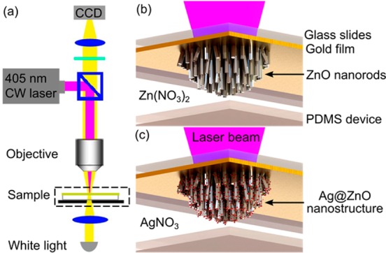
(a) Optical setups for fabricating 3D Ag@ZnO nanostructures in a microfluidic channel. Schematic illustration of on-chip, in situ creation of (b) ZnO nanorods and (c) Ag@ZnO nanostructures by optothermal effects.
Formation of ZnO Nanorods
As the scaffold of Ag@ZnO nanostructure fabrication, ZnO nanorods were synthesized by the optothermal effect. The formation mechanism was illustrated by a simulation of temperature and flow distribution near the laser spot area. The results (Figure 2) show that the parameters of the laser play important roles in determining the formation process of ZnO nanorods. First, the highest temperature reached is 385 K, with a heating power of 8.7 mW (similar to the heating power experimentally used), which is high enough for the hydrothermal synthesis of ZnO nanorods. The highest temperature locates at the glass/liquid interface (Figure 2a), where the gold film is situated. Second, the localized growth of ZnO nanorods at the laser spot area is induced by the sharp spatial distribution of the temperature along the microfluidic channel’s width (X-axis). For example, the temperature drops from 385 to 360 K as measurement shifted from the center of the focused laser spot to the boundary of the focused laser spot (about 20 μm) along the X direction. Further movement along the X-axis leads to a sharply reduced temperature, which is too low to satisfy the growth requirement of ZnO nanorods (Figure 2b). Third, the strong temperature gradient in the Y direction explains why the length of the ZnO nanorods was insensitive to the laser-irradiation time. The temperature decreases more significantly along the Y direction (Figure 2c); at a distance of 10 μm from the gold film, the temperature is insufficient for the growth of ZnO nanorods. Lastly, the heat-induced convective flow is also important to facilitate the formation of ZnO nanorods. Simulation results show that the amplitude of the convective flow (Figure 2a) from the bottom to the top inside the microfluidic channel was up to 10 μm/s. The convective flow draws precursor molecules to the laser-irradiation area, where they are consumed by the growth of ZnO nanorods. The effect of convective flow is confirmed experimentally by a shortened growth time of ZnO nanorods (∼5 min) compared to conventional hydrothermal methods in bulk reactions (∼30 min at 90 °C).
Figure 2.
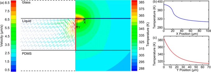
(a) Simulation results of the flow and temperature distributions during the optothermal effect. The temperature distributions along (b) X axis (the blue line in Figure 2a) and (c) Y axis (the red line in Figure 2a). The temperature decreases steeply from the laser spot area to the outside area, confining ZnO nanorod formation exclusively within the laser spot area.
A few minor discrepancies in temperature distribution exist between the simulations and the experiments. The highest temperature in the simulation (up to 385 K) is slightly above the boiling point of water, and this temperature is not observed in the experiments. This discrepancy is due to the overestimated energy input in the simulation. In the simulation, the power absorbed by the gold film is defined by subtracting the energy reflected from and transmitted through the gold film from the total energy of the laser beam. In reality, other factors, such as heat-transfer efficiency between different materials, make the heat power lower than that used in the simulation conditions. This trivial discrepancy does not influence the explanation of the optothermal growth process of the ZnO nanorods through the simulations. Overall, this simulation result confirms that the creation of ZnO nanorods is due to the optothermal effect. The inhomogeneous temperature distribution induces the localized formation of ZnO nanorods, while the convective flow facilitates the rapid preparation of ZnO nanorods.
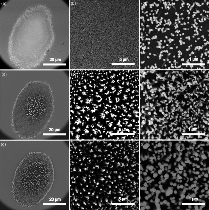
The morphology of the ZnO nanorods further supported the optothermal fabrication mechanism. The ZnO nanorods fabricated at laser-irradiation times of 5, 10, and 15 min were characterized by scanning electron microscopy (SEM). All ZnO nanorod clusters formed exclusively at the laser spot area, with an elliptical shape of about 40 × 30 μm (Figure 3a, d, g), consistent with the temperature distribution in the X direction. The ZnO nanorod cluster was composed of many densely packed, nearly vertical ZnO nanorods. The length of the ZnO nanorods was measured by observing lying nanorods induced by intentionally scratching the cluster after removing the PDMS device. All of the nanorods were about 1.0–1.5 μm in length, independent of the laser-irradiation time, which confirmed the strong temperature gradient in the Y direction. We also observed that when the irradiation time increased, the diameter of the ZnO nanorods increased significantly, while their packing density remained nearly constant. For example, the diameter of each hexagonal ZnO nanorod increased from 50 to 200 nm as the laser irradiation time was prolonged from 5 to 15 min. The density of the ZnO nanorods kept nearly constant at 50 nanorods per 1 μm2 when the laser-irradiation time exceeds 10 min. This phenomenon could be explained by the nucleation and growth theory,53,54 where ZnO was deposited on the preformed ZnO nanorods successively, rather than forming new ZnO nanorods. Initially, the gold film absorbed the laser energy to heat the surrounding precursor solutions. When the temperature of the solution reached a certain value, the ZnO component formed continuously until it oversaturated, which triggered the nucleation process. Since the ZnO component had the highest concentration on the laser-exposed area, which has the highest temperature, ZnO nanorods nucleated and grew on the hot region of the gold film. Once the nucleation process began, the growth of ZnO nanorods consumed the ZnO component in the solution, which prohibited further oversaturation of ZnO components. Thus, formation of new ZnO nuclei to increase the packing density became impossible.
Figure 3.
SEM images of ZnO nanorods fabricated at different laser-irradiation times with different magnifications: (a–c) 5 min; (d–f) 10 min; (g–i) 15 min.
The optothermal-effect-based fabrication strategy features several advantages: (1) This method enables significantly improved control over the location of fabrication compared to the conventional ZnO nanorod fabrication process in which the precursor solutions are heated in bulk reactors. The ZnO nanorods can therefore be incorporated inside any microfluidic device. (2) The optothermal effect allows fabrication of ZnO nanorods with a high packing density and well-defined structures. The morphology of the nanostructures can also be conveniently adjusted by the laser irradiation time, shape of the focusing spot, and the incidence power. (3) Optothermal-effect-based fabrication uses a thin layer of gold film as absorber, allowing a low-power continuous laser to create 3D Ag@ZnO structures rather than a high-power pulsed laser. Overall, the high packing density and uniformity of the ZnO nanorods make them excellent candidates as 3D SERS substrates with an exceptional sensing performance.
Formation of Ag@ZnO Nanostructures
Following the formation of ZnO, Ag nanoparticles were deposited on the preformed ZnO nanorods. The laser irradiation time for ZnO nanorod formation is 5 min, and the irradiation time for Ag nanoparticle deposition is 10 min. The mechanism of the deposition of silver nanoparticles is the decomposition of AgNO3 catalyzed by the optothermal effect. By focusing the laser beam on the ZnO nanorods, Ag nanoparticle deposition takes place only on the ZnO nanorods, resulting in the formation of 3D Ag@ZnO nanorods. The power of the laser for Ag deposition is lower (about 3 mW) than that for the growth of ZnO nanorods (15 mW) to regulate the reaction rate of the Ag nanoparticle deposition. The morphology of the ZnO nanorods remains unchanged during the Ag nanoparticle deposition because the temperature of the solution is much lower than that required in the ZnO formation process.
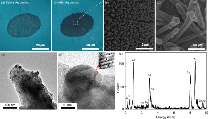
The deposition of Ag nanoparticles was first reflected by the color change under optical microscopy. The color of the ZnO nanorods turned from semitransparent (Figure 4a) to opaque (Figure 4b) due to the strong light absorption of Ag nanoparticles on the ZnO nanorods. The opaque color of the nanostructure indicated that, in Raman detection, the energy of the excitation laser could be used more efficiently by the 3D structures than 2D SERS substrates, such as various nanoparticle membranes. This improved efficiency indicates the benefit of the application of 3D structures in SERS sensing. The morphology of the Ag@ZnO nanostructure was further visualized by SEM (Figure 4c, d). The surface of the Ag@ZnO nanostructures was much coarser than that of the pure ZnO nanorods. Enlarged images revealed that there were numerous Ag nanoparticles randomly attached on the surfaces of the ZnO nanorods. The size of each Ag nanoparticle was several tens of nanometers.
Figure 4.
Morphology of Ag@ZnO nanostructure cluster. Optical images of ZnO nanorods (a) before and (b) after deposition of Ag nanoparticles for 10 min. (c) SEM image of Ag@ZnO nanorods. (d) Magnified SEM image of Ag@ZnO nanostructure. TEM images of (e) Ag@ZnO nanostructure and (f) a single Ag nanoparticle; (g) EDX element analysis of Ag@ZnO nanostructure.
To clearly observe the spatial arrangement and coverage of the Ag nanoparticles on the ZnO nanorods, transmission electron microscopy (TEM) characterizations were performed (Figure 4e). In the TEM image, a sharp contrast formed between ZnO nanorods and the Ag nanoparticles as a result of their different abilities to absorb electrons. Numerous Ag nanoparticles with sizes ranging from 10 to 40 nm were closely packed on the ZnO nanorods. The Ag nanoparticles were single crystalline, as verified by the high-resolution TEM result (Figure 4f). The lattice fingers of Ag (111) planes were clearly observable with a plane distance of 0.23 nm (Figure 4f, inset). Energy-dispersive X-ray spectroscopy (EDX) results further confirmed the existence of Ag and ZnO, consolidating the formation of the Ag@ZnO nanorod structures (Figure 4g). The small peaks of Au, Cu and C are from the gold film used for Ag@ZnO nanostructure preparation and the carbon-coated Cu mesh used as TEM sample holder.
Evaluation of SERS Performance
The SERS sensitivity of the 3D Ag@ZnO nanostructures was evaluated by detecting liquid-state 4-aminothiophenol (4-ATP) as a testing molecule. Here, the 3D Ag@ZnO with a 5 min laser-irradiation time was incorporated in the microfluidic channel as a SERS substrate. This irradiation time was used because it produced the best uniformity of ZnO nanorods in the center and at the edge of the ZnO nanorod clusters. High uniformity is important for improving the reproducibility of the SERS signals in sensing. As shown in Figure 5, strong SERS signals (black curve) were observed from 4-ATP molecules absorbed on the Ag@ZnO SERS substrates.55 In comparison, almost no observable SERS signals were detected from those 4-ATP molecules attached on either the thermally evaporated Au film (blue curve in Figure 5) or pristine ZnO nanorods before depositing Ag nanoparticles (red curve in Figure 5).
Figure 5.
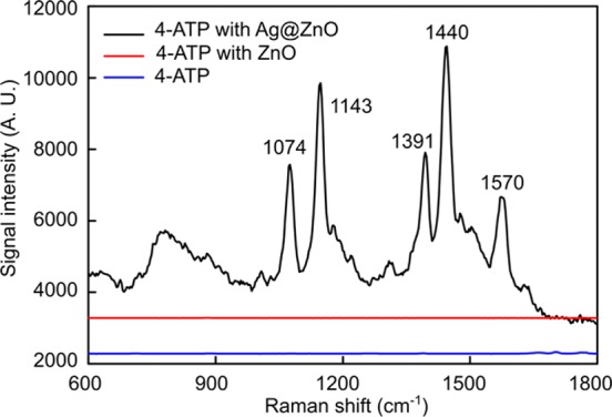
SERS spectra of 4-ATP using the 3D Ag@ZnO nanostructures as SERS substrates (black line); ZnO nanorods (red curve, up-shifted 3000); and with no SERS substrate (blue curve, up-shifted 2000).
The SERS enhancement factor (EF) of the Ag@ZnO nanostructures was estimated using the equation55
where ISERS is the Raman signal intensity of the 4-ATP molecules attached onto the Ag@ZnO nanostructures; Ibulk is the Raman signal intensity of solid 4-ATP powder; Nads is the number of 4-ATP molecules adsorbed on the Ag@ZnO nanostructures; Nbulk is the 4-ATP molecules that, in the solid state, are exposed to the laser light without Ag@ZnO nanostructures. Nbulk is estimated as a thin layer of 4-ATP powder with an area of 1 μm2 (area of laser-focusing spot) and depth of 20 μm (the penetration depth of the laser during SERS measurements). Considering the density (1.2 g/cm3) and the molecular weight (125 g/mol) of 4-ATP powder, Nbulk can be estimated to be about 1011. From the TEM results (Figure 5e), we can see that Ag nanoparticles with a wide size distribution are irregularly arranged on the ZnO nanorods. Although 4-ATP molecules can form a monolayer on the Ag nanoparticles, it is still difficult to accurately determine Nads due to the difficulties in defining the effective surface area of Ag. To simplify the estimation of Nads, we assume that ZnO nanorods are cylinder-shaped, with a diameter of 100 nm and length of 1.5 μm, and that they are arranged perpendicular to the substrate with packing density of 50 nanorods per 1 μm2. Thus, the total surface area of the 3D Ag@ZnO nanostructure is estimated as 2.4 × 10⁷ nm2 in 1 μm2. If we further assume a single layer of 4-ATP molecules attached on the Ag@ZnO nanostructures and the occupation area of a single 4-ATP molecule is about 0.5 nm2, Nads was estimated to be around 5 × 10⁷. ISERS/Ibulk was ∼103, observed by the SERS spectra (Figure 5). As such, the EF was calculated to be approximately 2 × 10⁶. It is worth mentioning that the calculated EF is inevitably underestimated, mainly due to the overestimation of the number of 4-ATP molecules on the Ag@ZnO nanostructures. Consequently, the real EF should be much higher.
The SERS effect was further confirmed theoretically by simulating the electromagnetic field distributions using FDTD software. The electromagnetic field distributions were simulated over ZnO nanorods, single Ag@ZnO structures, and neighboring Ag@ZnO structures with different distances (Figure 6). The electromagnetic field enhancement was trivial on pure ZnO nanorods (Figure 6a). In contrast, a strong electromagnetic field appeared close to the Ag nanoparticles attached to the ZnO nanorods (Figure 6b). Moreover, the electromagnetic field was magnified dramatically when two Ag@ZnO nanostructures approached each other (Figure 6c,d), arising from a significant amount of small crevices formed between Ag nanoparticles on the two nanorods. As a result, the 3D structure of the Ag@ZnO nanostructure clusters induced numerous SERS “hot spots” located between neighboring Ag nanoparticles on both the same ZnO nanorods (marked as 1 in Figure 6a) and adjacent ZnO nanorods (marked as 2 in Figure 6a).
Figure 6.
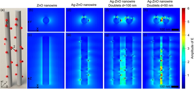
Electromagnetic field enhancement of ZnO nanorods and Ag@ZnO nanostructures using FDTD simulations. (a) Schematics of simulation configuration; (b, c) pristine ZnO nanorods showed limited electromagnetic field enhancements. (d, e) Ag@ZnO nanorods with strong electromagnetic field enhancements. (f, g) When two Ag@ZnO nanostructures are placed at a distance of 100 nm, the electromagnetic field is further magnified. (h, i) Further reduced distance between the Ag@ZnO nanorods gives rise to a dramatically enhanced electromagnetic field.
This unique 3D structure makes the Ag@ZnO nanostructure clusters good candidates for use in SERS sensing applications, giving rise to a strong SERS signal even when the analytes are in the liquid phase. In proof-of-concept studies, we tested BSA protein (0.01%, w/w) and DNA (single-stranded and hybridized double-stranded DNA, 1 μM) solutions with the 3D Ag@ZnO nanostructures (described in the Supporting Information). These results confirmed the ability to probe organic molecules such as proteins and DNAs, making our technique useful in environmental protection and medical diagnostics.
Single-Cell Trapping and SERS Fingerprinting
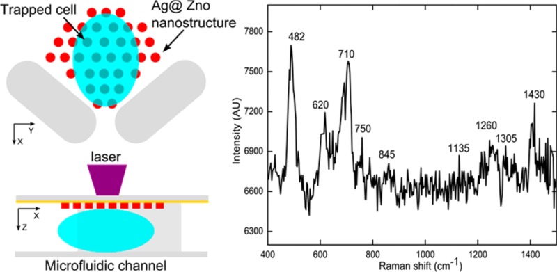
In this section, the SERS fingerprint of a single living cell surface was detected by integrating the 3D Ag@ZnO nanostructures with a single-cell trapping microfluidic device (Figure 7). In detail, the cell-trapping device (Figure 7a) is a horseshoe shaped trapper56−58 with three outlets (width of 10 μm). Since the size of each outlet is slightly smaller than a mature HeLa cell, when the cell suspension flows into the channel, a single cell can be trapped at the outlet. The Ag@ZnO nanostructures were fabricated close to the outlet inside the trapper (Figure 7a). The channel depth was carefully designed to be similar to the size of the cells (about 16 μm). Consequently, as cells were trapped within the horseshoe shaped structure, the cell surface was in close contact with the Ag@ZnO nanostructures, facilitating subsequent SERS measurements (Figure 7b). Three parallel outlets were used to improve the likelihood of successful cell trapping (Figure 7c). As anticipated, after flowing the HeLa cell suspension in PBS through the channel, a single cell was trapped on the top of each of the Ag@ZnO nanostructures (Figure 7d). SERS measurements were performed on the trapped cell with a 633 nm laser (about 1 mW) with an integration time of 20 s. SERS spectrum of the cell membrane (black curve in Figure 7e) reflected the fact that the cell surface is composed of proteins, carbohydrates, and lipids.59,60 For example, the peak located at 482 cm–1 is from the C–C–C deformation vibrations in carbohydrates; the 750 cm–1 peak arises from H–C–O stretches in carbohydrates; and hemiacetal stretches and methylene deformation lead to the appearance of the 845 cm–1 peak. The vibration peak from lipids can be found at 710 cm–1. SERS peaks from proteins are assigned to aliphatic side chains at 1430 cm–1 and the peptide backbone amide III at 1260 cm–1. Without the Ag@ZnO structures, no observable SERS peaks could be observed from Hela cells (red curve in Figure 7e).
Figure 7.
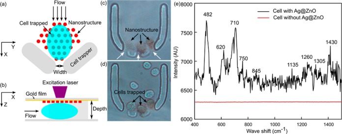
SERS fingerprinting of trapped single cells. Schematic demonstration of the cell-trapping device and the optothermal SERS substrate preparation concept in (a) X–Y plane and (b) X–Z plane; (c) Ag@ZnO nanorods were fabricated within the cell-trapping device; (d) single Hela cell were trapped at individual outlets of the horseshoe structure; (e) SERS peaks of cell surface with Ag@ZnO nanostructure (black line) and without Ag@ZnO nanostructures (red line).
The optothermal-effect-based fabrication technique allows us to fabricate sensitive SERS substrates at any desired location on-chip without necessary constraints to channel design. Therefore, it is convenient to integrate this SERS detection technique with most on-chip cell manipulation techniques61,62 into a single device to study cell behaviors (e.g., cell response to drugs). Additionally, the 3D Ag@ZnO nanostructure has good contact with the cell surface due to their highly complex shape. Accordingly, better SERS performance can be expected.
Conclusion
In summary, we have integrated SERS substrates composed of 3D Ag@ZnO nanostructures into microfluidic platforms. The growth of the Ag@ZnO nanostructure is through an optothermal-effect-based mechanism, which is confirmed by theoretical simulations of the temperature and flow distribution within and around the laser spot area. The Ag@ZnO nanostructures grow exclusively at the laser spot area, allowing for rational location control within the channel. Due to the dense Ag nanoparticles on the ZnO nanorods, substantial SERS hot-spots are integrated in the 3D Ag@ZnO nanorods, making them excellent candidates as SERS substrates. The SERS enhancement factor of the Ag@ZnO nanorods is estimated to be ∼2 × 10⁶ using 4-ATP as a test molecule. The integrated microfluidic-SERS system is validated by detecting low volumes of protein and DNA solutions. Furthermore, single-cell trapping and in situ SERS analysis are achieved through design of a horseshoe cell-trapping device and precisely growing Ag@ZnO nanorods within the horseshoe structure. Using our technique, cell surface biomarkers are visualized in real-time, without intake of any external SERS tags, minimizing potential damage on cell integrity. Overall, by unifying the advantages of SERS and microfluidics via our demonstrated optothermal fabrication technique, we expect that the integrated microfluidic-SERS system can be valuable in many chemical and biological analysis fields.
Materials and Methods
Chemicals
Zinc nitrate hexahydrate, hexamethylenetetramine (HMTA), and silver nitrate were purchased from Sigma-Aldrich with a grade of analytical purity for the synthesis of Ag@ZnO nanostructures. 4-Aminothiophenol (4-ATP), rhodamine 6G (R6G), and albumin from bovine serum (BSA) were purchased from Sigma-Aldrich as SERS detecting samples. The precursor solution for ZnO nanorod fabrication was a mixture of zinc nitrate (25 mM) and HMTA (25 mM). The precursor solution for Ag nanoparticle growth was a silver nitrate aqueous solution (20 mM).
Preparation of Microfluidic Channels
A polydimethylsiloxane (PDMS)-based microfluidic device was fabricated using standard soft lithography and mold replica techniques. Two types of microfluidic channels were used in the experiment. The device for the demonstration of nanostructure fabrication features the following dimensions: 10 mm in length, 10 mm in width, and 70 μm in depth. For cell trapping experiments, the channel comosed of a horseshoe-shaped trapper with three outlets (width of 10 μm) and a channel depth of 16 μm. Both microfluidic channels were prepared by bonding PDMS onto the gold-coated glass slide. The gold was thermally evaporated onto a glass slide (Semicore evaporator) with a thickness of 50 nm.
Fabrication of 3D Ag@ZnO Nanostructures
A diode laser (wavelength of 405 nm) was coupled to an upright optical microscope (Eclipse LV-100, Nikon, Japan). The objective lens (20 × , NA = 0.45) mounted on the microscope was used to focus the laser beam, as well as image the sample on a CCD camera (DS-Fi1, Nikon, Japan). The laser beam was focused into an elliptical area of approximately 30 × 40 μm on the gold film, serving as the bottom of the microfluidic device. The laser power was 15–20 mW, measured on the sample plane by a power meter (FieldMaxII-TO, Coherent, Santa Clara. CA). A motorized stage was used to move the PDMS channel and change the laser-focusing position and, therefore, the position of the prepared ZnO nanorods. The precursor solution for the ZnO nanorod fabrication was injected into the microfluidic channel with a syringe pump (KD Scientific, Waltham, MA). The growth of ZnO nanorods usually takes 5–15 min, depending on the experimental conditions.
Ag nanoparticles were deposited on ZnO nanorods using the same experimental setup as the one used for the fabrication of ZnO nanorods. The precursor solution (AgNO3; 20 mM) was injected into the microfluidic channel with a syringe pump to replace the ZnO precursor solutions. The laser spot was focused onto the ZnO nanorods to locally deposit Ag nanoparticles on them. The laser power was 3–5 mW. A laser exposure time of about 10 min was used to form 3D Ag@ZnO nanostructures.
On-Chip SERS Detection
4-ATP (1 μM), BSA (0.01%, w/w), and DNA (1 μM) were used to evaluate the SERS performance of the 3D Ag@ZnO nanorods. The analytes with desired concentrations were injected into the channel composed of 3D Ag@ZnO nanostructures, keeping them in a liquid state and a static flow condition. The Raman scattering spectra were recorded with a confocal microprobe Raman system with the excitation wavelength of 633 nm; the laser power was about 1 mW. The accumulation time was varied from 10 to 20 s, with different times corresponding to different samples. SERS measurements were repeated five times on the nanostructures and then averaged.
Trapping and SERS Detection of Single Cell
HeLa cells were grown in Dulbecco’s Modified Eagle Medium: Nutrient Mixture F-12 (DMEM/F12) media (Gibco, CA), supplemented with 10% fetal bovine serum (Atlanta Biologicals, GA), penicillin (100 U/mL), and 100 μg/mL streptomycin (Mediatech, VA). Cells ware grown to reach about 90% confluence before trypsinization (Trypsin +0.05% EDTA, Gibco, CA). After centrifugation (800 rpm for 5 min), cells were resuspended in a PBS buffer solution (1 × , pH 7.4) to reach a final concentration of about 2 × 10⁵ cells/ml. The suspension of the HeLa cells was injected into the microfluidic cell-trapping device at a flow rate of 10 μL/min. After cells were trapped within the horseshoe structures composed of pregrown 3D Ag@ZnO SERS substrates, the injecting flow was stopped. SERS measurements of the trapped cells were then performed using a 633 nm laser (about 1 mW) with an integrating time of 20 s.
Simulation of Temperature and Flow Fields
Numerical investigation was performed to simulate the temperature distribution and the convective flow around the laser spot area using Fluent software package. Since the laser beam was focused onto a small spot, the heating area could be considered as axisymmetrically distributed around the laser spot. As a result, an axisymmetrical 2D model was employed to reduce the simulation time. The whole model was built according to the device used in experiments, consisting of a glass slide, a thin water layer, and a PDMS layer. The thicknesses of the three layers were 150 μm, 70 μm, and 2 mm, respectively. The width of the three layers was 2 mm. To mimic the heating effect when the gold film absorbed the laser energy, a coupled thin film heat source with a thickness of 50 nm (the same as the gold film used in the experiments) was inserted at the glass/water interface. The radius of the coupled heat source was set to 20 μm, in accordance with the area of the focused laser beam. The heating power was 8.7 mW, which was determined by an optical test. As to the boundary conditions, the outer surfaces of both the glass layer and the PDMS layer were set as convective cooling surfaces. Convective cooling took place naturally at these two surfaces, thereby the heat transfer coefficients were given as 10 W/ (°C·m2). The conditions of the right sides of the three layers were set to the ambient temperature at 15 °C.
Simulation of Electromagnetic Field Enhancement
A finite-difference time-domain (FDTD) method (Lumerical, Inc., Canada) was used to simulate the electromagnetic field enhancement of ZnO and 3D Ag@ZnO nanostructures. The Ag@ZnO nanostructures were simplified as ZnO cylinders covered by randomly distributed spherical Ag nanoparticles. ZnO nanorods with a diameter of 100 nm and length of 1500 nm, revealed by the SEM observations, were used in the model for FDTD simulations. Silver nanoparticles with a diameter of 40 nm were randomly placed on the ZnO nanorods to imitate the 3D Ag@ZnO nanostructures. Two identical ZnO nanorods decorated with silver nanoparticles were separated by a distance of 50 or 100 nm to investigate the influence of the internanorod distance on the electromagnetic field distributions. A plane wave was used to illuminate the whole nanostructure immersed in a water solution.
Acknowledgments
We gratefully acknowledge financial support from the National Institutes of Health (Director’s New Innovator Award, 1DP2OD007209-01) and the Penn State Center for Nanoscale Science (MRSEC) under Grant No. DMR-0820404. Components of this work were conducted at the Penn State node of the NSF-funded National Nanotechnology Infrastructure Network.
The authors declare no competing financial interest.
Author Contributions
§ These authors contributed equally.
Supporting Information Available
Estimation of the laser energy input, on-chip detection of proteins and DNAs, and additional simulation results. This material is available free of charge via the Internet at http://pubs.acs.org.
Funding Statement
National Institutes of Health, United States
Supplementary Material
References
- Fang Y. Label-Free Biosensors for Cell Biology. Int. J. Electrochem. 2011, 2011, 1–16. [Google Scholar]
- Rapp B. E.; Gruhl F. J.; Länge K. Biosensors with Label-Free Detection Designed for Diagnostic Applications. Anal. Bioanal. Chem. 2010, 398, 2403–2412. [DOI] [PubMed] [Google Scholar]
- Houssin T.; Follet J.; Follet a; Dei-Cas E.; Senez V. Label-Free Analysis of Water-Polluting Parasite by Electrochemical Impedance Spectroscopy. Biosens. Bioelectron. 2010, 25, 1122–1129. [DOI] [PubMed] [Google Scholar]
- Rosman C.; Prasad J.; Neiser A.; Henkel A.; Edgar J.; Sönnichsen C. Multiplexed Plasmon Sensor for Rapid Label-Free Analyte Detection. Nano Lett. 2013, 13, 3243–3247. [DOI] [PubMed] [Google Scholar]
- Ngo H. T.; Wang H.-N.; Fales A. M.; Vo-Dinh T. Label-Free DNA Biosensor Based on SERS Molecular Sentinel on Nanowave Chip. Anal. Chem. 2013, 85, 6378–6383. [DOI] [PMC free article] [PubMed] [Google Scholar]
- Diakité M. L. Y.; Champ J.; Descroix S.; Malaquin L.; Amblard F.; Viovy J.-L. A Low-Cost, Label-Free DNA Detection Method in Lab-on-Chip Format Based on Electrohydrodynamic Instabilities, with Application to Long-Range PCR. Lab Chip 2012, 12, 4738–4747. [DOI] [PubMed] [Google Scholar]
- Zhang J. X. J.; Khademhosseini A. Emerging Micro- and Nanotechnologies in Cancer Diagnosis and Therapy. Biomed. Microdevices 2013, 15, 579–581. [DOI] [PubMed] [Google Scholar]
- Ayas S.; Cinar G.; Ozkan A. D.; Soran Z.; Ekiz O.; Kocaay D.; Tomak A.; Toren P.; Kaya Y.; Tunc I.; et al. Label-Free Nanometer-Resolution Imaging of Biological Architectures through Surface Enhanced Raman Scattering. Sci. Rep. 2013, 3, 2624. [DOI] [PMC free article] [PubMed] [Google Scholar]
- Råvik M.; Cimander C.; Elofsson U.; Veide A. A Method for Microbial Cell Surface Fingerprinting Based on Surface Plasmon Resonance. J. Biochem. Biophys. Methods 2007, 70, 595–604. [DOI] [PubMed] [Google Scholar]
- Stephen K. E.; Homrighausen D.; DePalma G.; Nakatsu C. H.; Irudayaraj J. Surface Enhanced Raman Spectroscopy (SERS) for the Discrimination of Arthrobacter Strains Based on Variations in Cell Surface Composition. Analyst 2012, 137, 4280–4286. [DOI] [PMC free article] [PubMed] [Google Scholar]
- Kumar R.; Vellanki S. H.; Smith R.; Wieder R. Determination of Single Cell Surface Protein Expression Using a Tagless Microfluidic Method. Lab Chip 2012, 12, 1646–1655. [DOI] [PubMed] [Google Scholar]
- Oh B.-R.; Huang N.-T.; Chen W.; Seo J. H.; Chen P.; Cornell T. T.; Shanley T. P.; Fu J.; Kurabayashi K. Integrated Nanoplasmonic Sensing for Cellular Functional Immunoanalysis Using Human Blood. ACS Nano 2014, 8, 2667–2676. [DOI] [PMC free article] [PubMed] [Google Scholar]
- Kroemer G.; Pouyssegur J. Tumor Cell Metabolism: Cancer’s Achilles’ Heel. Cancer Cell 2008, 13, 472–482. [DOI] [PubMed] [Google Scholar]
- Huh Y. S.; Chung A. J.; Erickson D. Surface Enhanced Raman Spectroscopy and Its Application to Molecular and Cellular Analysis. Microfluid. Nanofluidics 2009, 6, 285–297. [Google Scholar]
- Wei Q.; McLeod E.; Qi H.; Wan Z.; Sun R.; Ozcan A. On-Chip Cytometry Using Plasmonic Nanoparticle Enhanced Lensfree Holography. Sci. Rep. 2013, 3, 1699. [DOI] [PMC free article] [PubMed] [Google Scholar]
- Vashist S. K.; Mudanyali O.; Schneider E. M.; Zengerle R.; Ozcan A. Cellphone-Based Devices for Bioanalytical Sciences. Anal. Bioanal. Chem. 2014, 406, 3263–3277. [DOI] [PMC free article] [PubMed] [Google Scholar]
- Squires T.; Quake S. Microfluidics: Fluid Physics at the Nanoliter Scale. Rev. Mod. Phys. 2005, 77, 977–1026. [Google Scholar]
- Mao X.; Huang T. J. Microfluidic Diagnostics for the Developing World. Lab Chip 2012, 12, 1412–1416. [DOI] [PMC free article] [PubMed] [Google Scholar]
- Neuži P.; Giselbrecht S.; Länge K.; Huang T. J.; Manz A. Revisiting Lab-on-a-Chip Technology for Drug Discovery. Nat. Rev. Drug Discovery 2012, 11, 620–632. [DOI] [PMC free article] [PubMed] [Google Scholar]
- Xie Y.; Ahmed D.; Lapsley M. I.; Lin S. S.; Nawaz A. A.; Wang L.; Huang T. J. Single-Shot Characterization of Enzymatic Reaction Constants K. Anal. Chem. 2012, 84, 7495–7501. [DOI] [PMC free article] [PubMed] [Google Scholar]
- Huang P.-H.; Xie Y.; Ahmed D.; Rufo J.; Nama N.; Chen Y.; Chan C. Y.; Huang T. J. An Acoustofluidic Micromixer Based on Oscillating Sidewall Sharp-Edges. Lab Chip 2013, 13, 3847–3852. [DOI] [PMC free article] [PubMed] [Google Scholar]
- Zhao C.; Xie Y.; Mao Z.; Zhao Y.; Rufo J.; Yang S.; Guo F.; Mai J. D.; Huang T. J. Theory and Experiment on Particle Trapping and Manipulation via Optothermally Generated Bubbles. Lab Chip 2014, 14, 384–391. [DOI] [PMC free article] [PubMed] [Google Scholar]
- Ding X.; Lin S.-C. S.; Lapsley M. I.; Li S.; Guo X.; Chan C. Y.; Chiang I.-K.; Wang L.; McCoy J. P.; Huang T. J. Standing Surface Acoustic Wave (SSAW) Based Multichannel Cell Sorting. Lab Chip 2012, 12, 4228–4231. [DOI] [PMC free article] [PubMed] [Google Scholar]
- Ding X.; Lin S.-C. S.; Kiraly B.; Yue H.; Li S.; Chiang I.-K.; Shi J.; Benkovic S. J.; Huang T. J. On-Chip Manipulation of Single Microparticles, Cells, and Organisms Using Surface Acoustic Waves. Proc. Natl. Acad. Sci. U.S.A. 2012, 109, 11105–11109. [DOI] [PMC free article] [PubMed] [Google Scholar]
- Zhao J.; Liu Y.; Fales A. M.; Register J.; Yuan H.; Vo-Dinh T. Direct Analysis of Traditional Chinese Medicines Using Surface-Enhanced Raman Scattering (SERS). Drug Test. Anal. 2014, 6, 1063–1068. [DOI] [PubMed] [Google Scholar]
- Wachsmann-Hogiu S.; Weeks T.; Huser T. Chemical Analysis in Vivo and in Vitro by Raman Spectroscopy--from Single Cells to Humans. Curr. Opin. Biotechnol. 2009, 20, 63–73. [DOI] [PMC free article] [PubMed] [Google Scholar]
- Choo-Smith L.-P.; Edwards H. G. M.; Endtz H. P.; Kros J. M.; Heule F.; Barr H.; Robinson J. S.; Bruining H. a; Puppels G. J. Medical Applications of Raman Spectroscopy: From Proof of Principle to Clinical Implementation. Biopolymers 2002, 67, 1–9. [DOI] [PubMed] [Google Scholar]
- Choi I.; Huh Y. S.; Erickson D. Size-Selective Concentration and Label-Free Characterization of Protein Aggregates Using a Raman Active Nanofluidic Device. Lab Chip 2011, 11, 632–638. [DOI] [PubMed] [Google Scholar]
- Huh Y. S.; Erickson D. Aptamer Based Surface Enhanced Raman Scattering Detection of Vasopressin Using Multilayer Nanotube Arrays. Biosens. Bioelectron. 2010, 25, 1240–1243. [DOI] [PMC free article] [PubMed] [Google Scholar]
- Qian X.; Peng X.; Ansari D. O.; Yin-goen Q.; Chen G. Z.; Shin D. M.; Yang L.; Young A. N.; Wang M. D.; Nie S. In Vivo Tumor Targeting and Spectroscopic Detection with Surface-Enhanced Raman Nanoparticle Tags. Nat. Biotechnol. 2008, 26, 83–90. [DOI] [PubMed] [Google Scholar]
- Huang X.; El-sayed I. H.; Qian W.; El-sayed M. A. Cancer Cells Assemble and Align Gold Nanorods Conjugated to Antibodies to Produce Highly Enhanced, Sharp, and Polarized Surface Raman Spectra: A Potential Cancer Diagnostic Marker. Nano Lett. 2007, 7, 1591–1597. [DOI] [PubMed] [Google Scholar]
- Yan B.; Reinhard B. M. Identification of Tumor Cells through Spectroscopic Profiling of the Cellular Surface Chemistry. J. Phys. Chem. Lett. 2010, 1, 1595–1598. [Google Scholar]
- Yang S.; Cai W.; Kong L.; Lei Y. Surface Nanometer-Scale Patterning in Realizing Large-Scale Ordered Arrays of Metallic Nanoshells with Well-Defined Structures and Controllable Properties. Adv. Funct. Mater. 2010, 20, 2527–2533. [Google Scholar]
- Yang S.; Lapsley M. I.; Cao B.; Zhao C.; Zhao Y.; Hao Q.; Kiraly B.; Scott J.; Li W.; Wang L.; et al. Large-Scale Fabrication of Three-Dimensional Surface Patterns Using Template-Defined Electrochemical Deposition. Adv. Funct. Mater. 2013, 23, 720–730. [DOI] [PMC free article] [PubMed] [Google Scholar]
- Yang S.; Xu F.; Ostendorp S.; Wilde G.; Zhao H.; Lei Y. Template-Confined Dewetting Process to Surface Nanopatterns: Fabrication, Structural Tunability, and Structure-Related Properties. Adv. Funct. Mater. 2011, 21, 2446–2455. [Google Scholar]
- Qi J.; Motwani P.; Gheewala M.; Brennan C.; Wolfe J. C.; Shih W.-C. Surface-Enhanced Raman Spectroscopy with Monolithic Nanoporous Gold Disk Substrates. Nanoscale 2013, 5, 4105–4109. [DOI] [PubMed] [Google Scholar]
- Li M.; Lu J.; Qi J.; Zhao F.; Zeng J.; Yu J. C.-C.; Shih W.-C. Stamping Surface-Enhanced Raman Spectroscopy for Label-Free, Multiplexed, Molecular Sensing and Imaging. J. Biomed. Opt. 2014, 19, 50501. [DOI] [PubMed] [Google Scholar]
- Leem J.; Kang H. W.; Mahmood K.; Sung H. J. Controllable Ag Nanostructure Patterning in a Microfluidic Channel for Real-Time SERS Systems. Nanoscale 2014, 6, 2895–2901. [DOI] [PubMed] [Google Scholar]
- Lyandres O.; Shah N. C.; Yonzon C. R.; Walsh J. T.; Glucksberg M. R.; Van Duyne R. P. Real-Time Glucose Sensing by Surface-Enhanced Raman Spectroscopy in Bovine Plasma Facilitated by a Mixed Decanethiol/mercaptohexanol Partition Layer. Anal. Chem. 2005, 77, 6134–6139. [DOI] [PubMed] [Google Scholar]
- Xia X.; Li W.; Zhang Y.; Xia Y. Silica-Coated Dimers of Silver Nanospheres as Surface-Enhanced Raman Scattering Tags for Imaging Cancer Cells. Interface Focus 2013, 3, 20120092. [DOI] [PMC free article] [PubMed] [Google Scholar]
- Rycenga M.; Xia X.; Moran C. H.; Zhou F.; Qin D.; Li Z.; Xia Y. Generation of Hot Spots with Silver Nanocubes for Single-Molecule Detection by Surface-Enhanced Raman Scattering. Angew. Chem., Int. Ed. 2011, 5473–5477. [DOI] [PMC free article] [PubMed] [Google Scholar]
- Mao H.; Wu W.; She D.; Sun G.; Lv P.; Xu J. Microfluidic Surface-Enhanced Raman Scattering Sensors Based on Nanopillar Forests Realized by an Oxygen-Plasma-Stripping-of-Photoresist Technique. Small 2014, 10, 127–134. [DOI] [PubMed] [Google Scholar]
- Liu G. L.; Lee L. P. Nanowell Surface Enhanced Raman Scattering Arrays Fabricated by Soft-Lithography for Label-Free Biomolecular Detections in Integrated Microfluidics. Appl. Phys. Lett. 2005, 87, 074101. [Google Scholar]
- Oh Y.-J.; Jeong K.-H. Optofluidic SERS Chip with Plasmonic Nanoprobes Self-Aligned along Microfluidic Channels. Lab Chip 2014, 14, 865–868. [DOI] [PubMed] [Google Scholar]
- MacFarlane P. D.; Tute a S.; Alderson B. Therapeutic Options for the Treatment of Chronic Pain in Dogs. J. Small Anim. Pract. 2014, 55, 127–134. [DOI] [PubMed] [Google Scholar]
- Piorek B. D.; Lee S. J.; Moskovits M.; Meinhart C. D. Free-Surface Micro Fl uidics/Surface-Enhanced Raman Spectroscopy for Real-Time Trace Vapor Detection of Explosives. Anal. Chem. 2012, 84, 9700–9705. [DOI] [PubMed] [Google Scholar]
- Park H. K.; Yoon J. K.; Kim K. Novel Fabrication of Ag Thin Film on Glass for Efficient Surface-Enhanced Raman Scattering. Langmuir 2006, 22, 1626–1629. [DOI] [PubMed] [Google Scholar]
- Park H. K.; Lee H. B.; Kim K. A Facile Deposition of Silver onto the Inner Surface of a Glass Capillary Tube for Micro-Surface-Enhanced Raman Scattering Measurements. Appl. Spectrosc. 2007, 61, 19–24. [DOI] [PubMed] [Google Scholar]
- Xu B.-B.; Zhang R.; Liu X.-Q.; Wang H.; Zhang Y.-L.; Jiang H.-B.; Wang L.; Ma Z.-C.; Ku J.-F.; Xiao F.-S.; et al. On-Chip Fabrication of Silver Microflower Arrays as a Catalytic Microreactor for Allowing in Situ SERS Monitoring. Chem. Commun. (Camb). 2012, 48, 1680–1682. [DOI] [PubMed] [Google Scholar]
- Xu B.-B.; Ma Z.-C.; Wang H.; Liu X.-Q.; Zhang Y.-L.; Zhang X.-L.; Zhang R.; Jiang H.-B.; Sun H.-B. A SERS-Active Microfluidic Device with Tunable Surface Plasmon Resonances. Electrophoresis 2011, 32, 3378–3384. [DOI] [PubMed] [Google Scholar]
- Xu B.-B.; Ma Z.-C.; Wang L.; Zhang R.; Niu L.-G.; Yang Z.; Zhang Y.-L.; Zheng W.-H.; Zhao B.; Xu Y.; et al. Localized Flexible Integration of High-Efficiency Surface Enhanced Raman Scattering (SERS) Monitors into Microfluidic Channels. Lab Chip 2011, 11, 3347–3351. [DOI] [PubMed] [Google Scholar]
- Betz J. F.; Yu W. W.; Cheng Y.; White I. M.; Rubloff G. W. Simple SERS Substrates: Powerful, Portable, and Full of Potential. Phys. Chem. Chem. Phys. 2014, 16, 2224–2239. [DOI] [PubMed] [Google Scholar]
- Search H.; Journals C.; Contact A.; Iopscience M.; Address I. P. Nucleation and Growth of Thin Films. Rep. Prog. Phys. 1984, 47, 399–459. [Google Scholar]
- Yoreo J. J. De; Vekilov P. G. Principles of Crystal Nucleation and Growth. Rev. Mineral. Geochemistry 2003, 54, 57–93. [Google Scholar]
- Hu X.; Wang T.; Wang L.; Dong S. Surface-Enhanced Raman Scattering of 4-Aminothiophenol Self-Assembled Monolayers in Sandwich Structure with Nanoparticle Shape Dependence: Off-Surface Plasmon Resonance Condition. J. Phys. Chem. C 2007, 111, 6962–6969. [Google Scholar]
- Ahmed D.; Mao X.; Shi J.; Juluri B. K.; Huang T. J. A Millisecond Micromixer via Single-Bubble-Based Acoustic Streaming. Lab Chip 2009, 9, 2738–2741. [DOI] [PubMed] [Google Scholar]
- Xie Y.; Ahmed D.; Lapsley M. I.; Lu M.; Li S.; Huang T. J. Acoustofluidic Relay: Sequential Trapping and Transporting of Microparticles via Acoustically Excited Oscillating Bubbles. J. Lab. Autom. 2014, 19, 137–143. [DOI] [PubMed] [Google Scholar]
- Ahmed D.; Chan C. Y.; Lin S.-C. S.; Muddana H. S.; Nama N.; Benkovic S. J.; Huang T. J. Tunable, Pulsatile Chemical Gradient Generation via Acoustically Driven Oscillating Bubbles. Lab Chip 2013, 13, 328–331. [DOI] [PMC free article] [PubMed] [Google Scholar]
- Huang W. E.; Ward A. D.; Whiteley A. S. Raman Tweezers Sorting of Single Microbial Cells. Environ. Microbiol. Rep. 2009, 1, 44–49. [DOI] [PubMed] [Google Scholar]
- Wu H.; Volponi J. V.; Oliver A. E.; Parikh A. N.; Simmons B. a; Singh S. In Vivo Lipidomics Using Single-Cell Raman Spectroscopy. Proc. Natl. Acad. Sci. U.S.A. 2011, 108, 3809–3814. [DOI] [PMC free article] [PubMed] [Google Scholar]
- Lin S.-C. S.; Mao X.; Huang T. J. Surface Acoustic Wave (SAW) Acoustophoresis: Now and Beyond. Lab Chip 2012, 12, 2766–2770. [DOI] [PMC free article] [PubMed] [Google Scholar]
- Chiou P. Y.; Ohta A. T.; Wu M. C. Massively Parallel Manipulation of Single Cells and Microparticles Using Optical Images. Nature 2005, 436, 370–372. [DOI] [PubMed] [Google Scholar]
Associated Data
This section collects any data citations, data availability statements, or supplementary materials included in this article.


