Abstract
A capacitive charge-division readout method for reading out a 2 × 2 array of 5 mm × 5 mm position-sensitive solid-state photomultipliers (PS-SSPM) was designed and evaluated. Using this analog multiplexing method, the 20 signals (16 position, 4 timing) from the PS-SSPM array are reduced to 5 signals (4 position, 1 timing), allowing the PS-SSPM array to be treated as an individual large-area PS-SSPM module. A global positioning approach can now be used, instead of individual positioning for each PS-SSPM in the array, ensuring that the entire light signal is utilized. The signal-to-noise ratio (SNR) and flood histogram quality at different bias voltages (27.5 V to 32.0 V at 0.5 V intervals) and a fixed temperature of 0 °C were evaluated by coupling a 6 × 6 array of 1.3 mm × 1.3 mm × 20 mm polished LSO crystals to the center of the PS-SSPM array. The timing resolution was measured at a fixed bias voltage of 31.0 V and a fixed temperature of 0 °C. All the measurements were evaluated and compared using capacitors with different values and tolerances. Capacitor values ranged from 0.051 nf to 10 nf, and the capacitance tolerance ranged from 1% to 20%. The results show that better performance was achieved using capacitors with smaller values and better capacitance tolerance. Using 0.2 nf capacitors, the SNR, energy resolution and timing resolution were 24.3, 18.2% and 8.8 ns at a bias voltage 31.0 V, respectively. The flood histogram quality was also evaluated by using a 10 × 10 array of 1 mm × 1 mm × 10 mm polished LSO crystals and a 10 × 10 array of 0.7 mm × 0.7 mm × 20 mm unpolished LSO crystals to determine the smallest crystal size resolvable. These studies showed that the high spatial resolution of the PS-SSPM was preserved allowing for 0.7 mm crystals to be identified. These results show that the capacitive charge-division analog signal processing method can significantly reduce the number of electronic channels, from 20 to 5, while retaining the excellent performance of the detector.
Index Terms: PET, PS-SSPM, Electronics, Capacitive Charge–Division Readout
I. Introduction
Solid-state photomultipliers (SSPMs) [1], also referred to as silicon-photomultipliers (SiPMs) or multi-pixel photon counters (MPPCs) [2]-[3], are advantageous compared to PMTs and APDs, because of their high gain and insensitivity to magnetic fields. A novel 2 × 2 position-sensitive SSPM (PS-SSPM) array (Fig. 1) was designed and developed in collaboration with RMD (Radiation Monitoring Devices, Inc.). This photodetector can resolve sub-millimeter scintillation arrays making it ideal for high resolution small-animal PET detector designs [4]. The physical size of this device is 10.0 mm × 10.0 mm. The individual size of each PS-SSPM in the array is 4.9 mm × 4.9 mm, with ~ 0.2 mm dead space between them. Analogous to position-sensitive avalanche photodiode (PS-APD) readout [5], each individual PS-SSPM requires five electronic channels to extract the interaction information, four corner anode signals with position information and one cathode signal for timing. In total the 2 × 2 detector array therefore requires 20 readout channels, 16 anodes channels for position and energy and 4 cathode channels for timing. Discretely shaping and digitizing each channel is cumbersome and expensive, especially when considering scaling to a PET scanner utilizing this photodetector. Therefore a simple, but high performance, multiplexer is needed to reduce the number of detector readout channels.
Fig. 1.
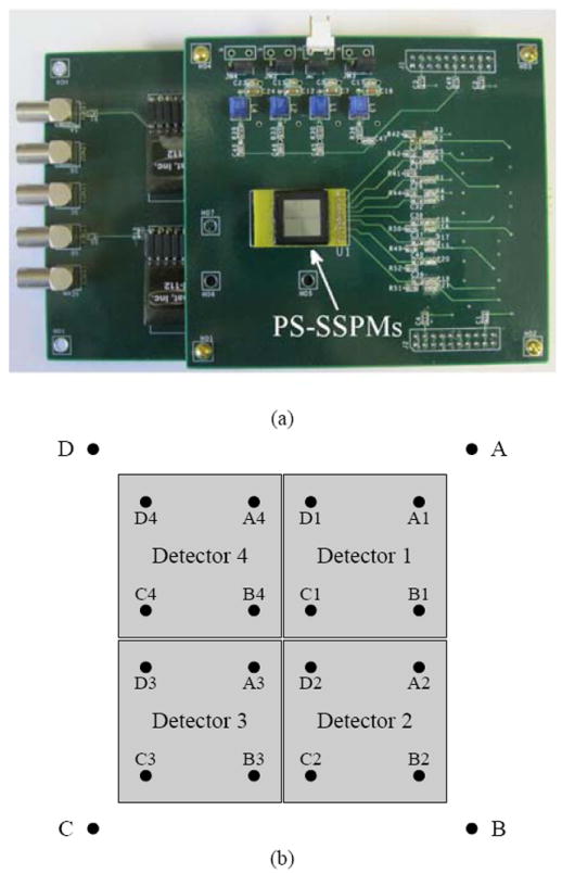
(a) PS-SSPMs with the capacitive-charge division readout and preamplifier board and (b) schematic of PS-SSPMs outputs and naming convention.
Many multiplexing methods have been designed and evaluated by different research groups [6]-[14]. All of these methods, except Lau’s method [10], are designed for an array of single channel detectors, such as a multi-anode PMT or SiPM array, not for a position-sensitive detector array such as the one presented and described in [4]. Lau’s method [10], which is similar to SensL’s cross-wired readout architecture [14], can be used for a position-sensitive detector array and requires N + 4 electronic channels for a detector array with N detectors. For our 2 × 2 PS-SSPM array, eight electronic signals would be needed, four energy signals to determine the γ interaction position and four cathode signals to determine which detector is fired. Therefore, four discriminators (constant fraction discriminator or leading edge discriminator) are necessary to identify which detector is fired. Our multiplexing approach is completely different from the above referenced methods and uses a capacitive charge-division readout circuit, which reduces the number of readout channels from 20 to 5 (4 channels for position and energy and 1 channel for timing), or from 1 electronic channel per 5 mm2 to 1 electronic channel per 20 mm2 of detector area. In addition, this circuit allows the 2 × 2 PS-SSPM array to be treated as a continuous detector module, hence all the electronics and data processing software for one individual PS-SSPM can be used to process the data from the 2 × 2 PS-SSPM array. Because the performance of the capacitive charge-division readout circuit is related to the capacitors used, including the capacitor value and the capacitance tolerance [15]-[16], capacitors with eight different values (0.051 nf, 0.1 nf, 0.2 nf, 0.51 nf, 1 nf, 2 nf, 5.1 nf and 10 nf, tolerance is 5%) and capacitors with five different tolerances (1%, 2%, 5%, 10%, 20%) for a fixed capacitor value of 220 pf value were studied experimentally. Performance of this capacitive charge-division circuit was analyzed by measuring signal-to-noise ratio (SNR) [5], energy resolution, quality of flood histogram, and timing resolution at different bias voltages (28.0 V to 32.0 V at 0.5 V intervals) and at a fixed temperature of 0 °C.
II. Material and Methods
A. PS-SSPM and Crystal Array
A 6 × 6 polished LSO array, with a crystal pitch of 1.3 mm and a length of 20 mm, separated by enhanced specular reflector (3M, St Paul, MN), was used to measure SNR, energy resolution, flood histogram quality, and timing resolution. A 10 × 10 array of 1 mm× 1 mm × 10 mm polished LSO crystals, with ESR reflector and a 10 × 10 array of 0.7 mm × 0.7 mm × 20 mm unpolished LSO crystals, with Toray lumirror E60 film reflector were also used in the flood histogram measurement. The 1 mm and 0.7 mm arrays were used to investigate the crystal identification ability of the capacitive charge-division circuit.
The detector was mounted on custom made readout boards, which consisted of the capacitive charge-division board and a preamplifier board. A picture of the PS-SSPM array mounted on the readout boards is shown in Fig. 1(a), with a diagram of the location of the 16 anode channels shown in Fig. 1(b).
The LSO array, detector, and readout boards were placed inside a light tight box connected to ground. The detector temperature was controlled using an air-jet crystal cooler (FTS Systems, Inc, Stone Ridge, NY) and monitored by a Type K thermocouple (DigiSense, Inc). The probe of the thermocouple was placed less than 10 mm from the detector to ensure an accurate measurement of the air temperature near the detector. This temperature was maintained at 0°C for all measurements.
The crystals were irradiated using a 20 uCi 22Na point source, placed 10 mm above the front face of the LSO array. The source was moved for the timing measurement, and was placed centrally between the PS-SSPM array and the PMT detector with a center-to-center distance of ~200 mm.
B. Capacitive Charge-Division Circuit
A schematic of the capacitive charge-division circuit is shown in Fig. 2. The signals A1 - D4 correspond to the definition in Fig. 1(b). The relationship between the four final positioning signals A, B, C and D and the position signals (anode signals) of each PS-SSPM are as follows:
| (1) |
Fig. 2.
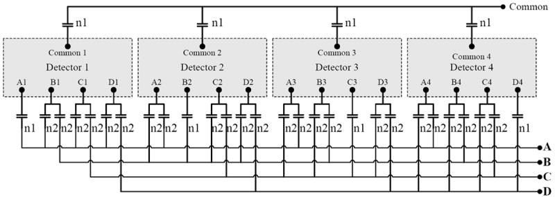
Schematic of the capacitive charge-division readout method. The 49.9 ohm load resistors for each anode output are not shown in this picture.
Using this transformation (Eq. 1) the 2 × 2 array of detectors can be treated as an individual position-sensitive detector module and the γ photon interaction position can be calculated by using standard Anger logic equations as:
| (2) |
The four cathode signals are connected directly through four capacitors and combined to form one signal, which was used as the trigger and timing signal. To ensure that each anode signal and each following pre-amplifier sees the same capacitance, the AC coupling capacitor value n1 should be twice that of n2 (see Fig. 2). In our readout design, each individual PS-SSPM can be powered separately by four independent power supplies. It was observed that the PS-SSPMs in the array are very homogenous in terms of breakdown voltage, signal, and noise properties [4]. Therefore to simplify the design only one power supply was used and divided into four sources which were individually filtered by π filters (C-L-C) to isolate the crosstalk effect from other channels on board, as shown in Fig. 3.
Fig. 3.
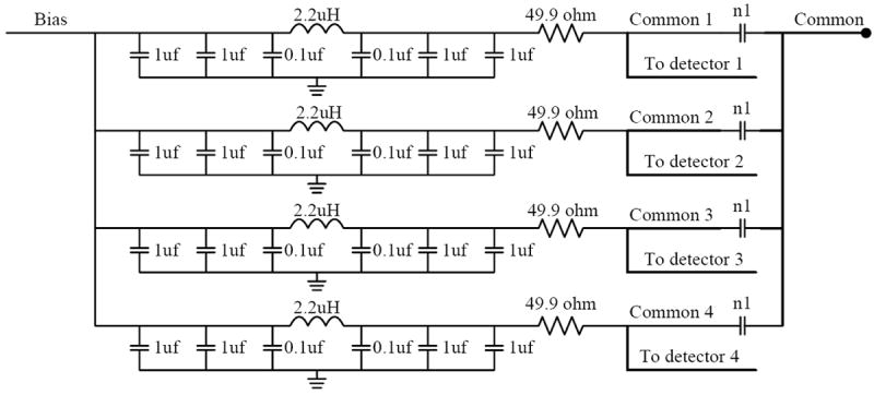
Schematic for the bias supply and common signal.
Because the capacitor value affects the signal received by the pre-amplifiers [15]-[16], capacitors with eight different values were experimentally studied. The capacitor values for n2 were 0.051 nf, 0.1 nf, 0.2 nf, 0.51 nf, 1 nf, 2 nf, 5.1 nf and 10 nf, and the corresponding n1 values were 0.102 nf, 0.2 nf, 0.4 nf, 1.02 nf, 2 nf, 4 nf, 10.2 nf and 20 nf. In the proposed capacitive charge-division method, the AC capacitors are also used to split the signal into two equal parts. The tolerance of the selected capacitors will affect this signal splitting, hence, capacitors with five different capacitance tolerances (1%, 2%, 5%, 10%, 20%) were also studied experimentally when capacitors with values of 0.22 nf and 0.44 nf were used for n2 and n1 respectively. All the selected capacitors were made from C0G/NP0 material except the capacitors with 20% tolerance, which were made from X7R material. Compared to X7R material, the C0G/NP0 material is more stable when working at different temperatures and voltages.
C. Detector Readout and Data Analysis
After multiplexing, the final four position signals A, B, C and D were all fed into Cremat CR-112 preamplifiers. The outputs were further amplified and shaped by a Caen spectroscopy amplifier (N568B) before being digitized by a PowerDAQ board [17]. The gain of the N568B was fixed for all tests. An Ortec 579 fast filter amplifier and Ortec 584 constant fraction discriminator (CFD) were used on the cathode channel to extract timing information, and also to provide a trigger signal for the PowerDAQ board.
The SNR was measured following the methods described in [4] and [5]. Briefly, the noise was quantified using the FHWM of a Gaussian fit to the noise distribution (summed noise from the four position signals A, B, C and D acquired by triggering the PowerDAQ using the internal trigger generated by the computer clock) and the 511 keV photopeak amplitude was treated as the signal (external trigger). While the noise has several potential sources, in these measurements it likely originates from the detector dark count rate which increases with bias voltage due to the increased Geiger discharge probability. The signal amplitude was calculated from the global energy spectrum after correcting for the channel offsets, which was done by subtracting the peak position of the noise distribution. The SNR was then calculated from these values. The main goal of the SNR measurements was to find an optimal operating bias voltage. The effect of temperature was not studied; for all measurements the air temperature measured a fixed distance from the detector was held at 0 °C. The data generated for the SNR measurements was also used to calculate the energy resolution and the flood histogram quality. For this study, energy resolution was calculated from the global energy spectrum and not on an individual crystal basis.
To compare the flood histogram quality, a flood histogram quality parameter was calculated by comparing the peak position and the spot width of adjacent crystals in the flood using the following function:
| (3) |
where wxi and wyi are the FWHMs of the x and y projections of the ith crystal, and xi and yi are the centroids of the x and y projections of the ith crystal. Due to the symmetry of the detector and the crystal array only nine crystals, instead of all the thirty-six crystals, were used as shown in Fig. 4.
Fig. 4.
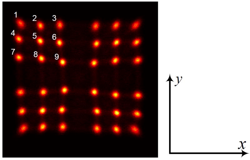
The nine crystals indicated which are coupled to one PS-SSPM were used to calculate the flood histogram quality.
The PS-SSPM timing resolution was measured at a bias voltage of 31.0 V, the optimal value determined by the SNR results. The reference detector was composed of a single channel Hamamatsu PMT R6231 coupled to an LSO block (13 mm × 13 mm × 20 mm). The PMT signal was fed into a LeCroy 612 PMT amplifier directly and an Ortec 584 CFD for time pick off. The PMT time trigger was used as the start signal and the PS-SSPM time trigger was used as a stop signal for the TAC (Tennelec TC 863). The timing resolution of the reference detector was estimated to be 1.7 ns, which is far superior to the timing resolution of the PS-SSPM detector that was being evaluated. A crystal look up table was applied to the flood histogram to create individual timing spectra for each crystal. The global timing resolution was calculated by taking the same number of events from each crystal in the crystal array. This eliminated effects from non-uniformities in the efficiencies for different crystals. The FWHM of a Gaussian fit to the timing spectra was used as the measure of the timing resolution. Timing resolution was compared using the different capacitor values. For each capacitor value, the timing resolution was quantified in several ways by post processing of the data using a 200 keV lower energy threshold, by applying an energy window of 400 - 650 keV, and with and without a crystal timing shift calibration [18]. The timing shift calibration corrects for the position- dependent offsets in pulse arrival time due to the resistive readout of the PS-SSPM.
III. Results
A. Pulse Shape
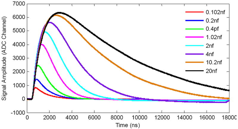
Fig. 5 shows the pulse shape and amplitude of the cathode signal after amplification by the Cremat CR-112 preamplifier when different capacitor values were used at a bias voltage of 31.0 V. The legends on the figure are for the value of capacitor n1, which is twice the value of n2. The pulse shapes are the average of 50 pulses captured by the oscilloscope DPO7254 (Tektronix, Inc.).
Fig. 5.
Average pulse shape and amplitude.
To generate the pulse shapes shown in Fig. 5, the amplitudes of the 50 pulses corresponding to a particular capacitor value were first individually normalized and then summed to give an average pulse. The amplitude was then scaled using the measured amplitude of the 511 keV photopeak for each capacitor value.
From Fig. 5, it is obvious that when capacitors with smaller values were used, the signal rise time and fall time are much faster, but the signal amplitude is smaller. For a high count rate environment, capacitors with smaller values can reduce signal pileup.
B. Signal-to-Noise
Fig. 6 shows the signal, noise and the SNR versus bias voltage and capacitor value. The noise includes noise caused by the pre-amplifier and NIM module, which was ~8.6 ADC channels. Both noise and signal increase as capacitor value and bias voltage increase. The noise increase with increasing bias voltage is mainly caused by the increased Geiger discharge probability. SNR increases sharply at low bias voltages and at higher bias voltages becomes fairly flat. There is a slight decrease in SNR at the highest bias voltages tested. SNR at bias voltages higher than 32.0 V were not studied due to risk of disrupting the junction. The best SNR was achieved at a bias voltage of 31.0 V for each capacitor value except 5.1 nf and 10 nf capacitors. The best SNR for these two capacitor values was achieved at a bias voltage of 29.0 V.
Fig. 6.
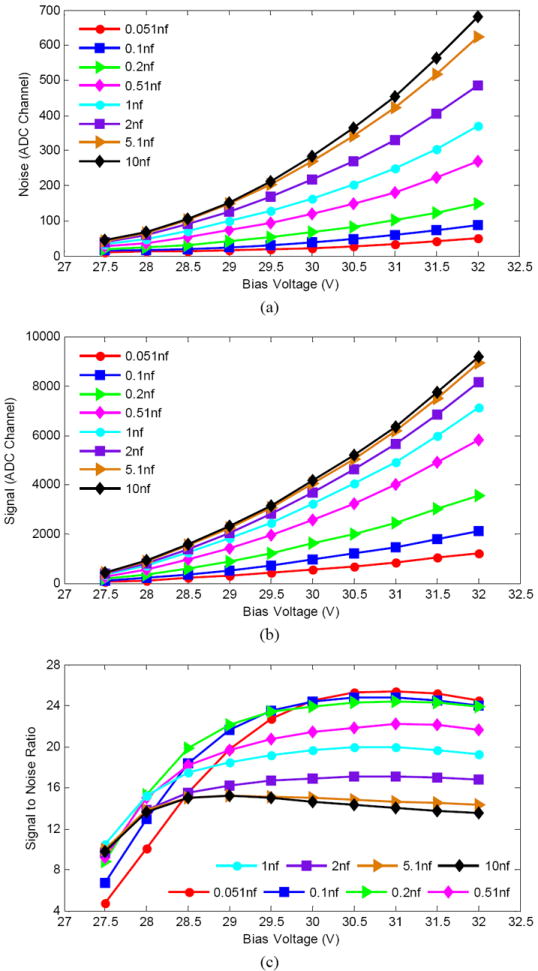
(a) noise, (b) signal and (c) SNR versus bias voltage and capacitor value.
An explanation for the changes in signal and noise for different capacitor values is as follows:
lower capacitance will cause smaller serial noise to the following amplifier CR-112 [15];
- if the PS-SSPM is treated as an ideal current source in parallel with a capacitor (Cd) and a resistor (Rd) [16], assuming the signal frequency is s, then the ratio of the current flowing to the pre-amplifier to the total current will be:
(4) - the PS-SSPM and the AC capacitor (n1) together with the feedback capacitor (Cf) and resistor (Rf) of the amplifier will form a bandpass filter [16]. The low (fl) and high (fh) cutoff frequencies of this filter are related to Cd, n1, Rd, Rf, Cf as follows:
(5)
For lower capacitance values, more noise can be filtered out, however the low-frequency part of the signal also will be filtered out. Therefore, the total received signal will be smaller.
Combining these three effects, both the signal and the noise will increase with larger capacitor values. The best SNR was obtained with lower capacitor values (Fig. 6c).
Fig. 7 shows the noise, signal and SNR when capacitors with different tolerances were used; the capacitor values of n1 and n2 were fixed at 0.22 nf and 0.44 nf respectively. The signal and noise does not vary significantly with changes in capacitor tolerance, however SNR is slightly improved with 1% tolerance compared to 20% tolerance capacitors. Compared to X7R material (20% tolerance capacitors), C0G/NP0 (all other tolerances) is more stable across different temperatures and voltages. At lower temperatures, the capacitance of X7R capacitors is less than the nominal capacitance. Hence, the noise and signal are smaller. The SNR from different capacitors are almost the same, with a trend of better SNR for the capacitors with 1% tolerance.
Fig. 7.
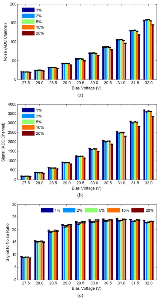
(a) noise, (b) signal and (c) SNR versus bias voltage and capacitive tolerance. The error bars correspond to the gaussian fitting error.
C. Energy Resolution
The measurements of energy resolution versus bias voltage and capacitor value are illustrated in Fig. 8(a). The energy resolution initially improves sharply with increasing bias voltage, but does not improve significantly for bias voltages above ~30.0 V for each capacitor value. The best energy resolution of 18.3% was achieved when 0.2 nf capacitors were used at 31.0 V bias voltage.
Fig. 8.

Energy resolution versus bias voltage and (a) capacitor value and (b) capacitor tolerance.
The energy resolution versus bias voltage and capacitor tolerance is plotted in Fig. 8(b). At lower bias voltage, the energy resolution is more dependent on capacitor tolerance than at higher bias voltage and the best energy resolution is obtained using capacitors with 1% tolerance up to a bias voltage of 31.0 V.
D. Flood Histograms
The flood histograms and the flood histogram quality versus bias voltage and capacitor value are shown in Fig. 9 and Fig.10 respectively. The four signals A, B, C, D have been calibrated by subtracting the offsets before calculating the gamma photon interaction position. Flood histogram quality first increases and then decreases slightly as the bias voltage increases. Better flood histogram quality was obtained using capacitors with smaller values. The SNR curve (Fig. 6(c)) and flood histogram quality curves (Fig. 10) are quite similar, indicating that better flood histogram can be obtained when the signal-to-noise ratio is higher, matching results described in [5] and [19].
Fig.9.
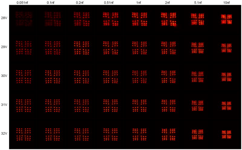
Flood histograms versus bias voltage and capacitor value.
Fig.10.
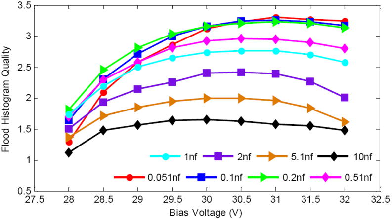
Flood histogram quality versus bias voltage and capacitor value.
Fig. 11 illustrates the flood histograms and the flood histogram quality versus bias voltage and capacitor tolerance. Visually, it is hard to discern differences in the flood histogram quality for different capacitor tolerances, but the measured flood histogram quality metric shows that better flood histogram quality was obtained using capacitors with a better tolerance. This is anticipated, as capacitors with better tolerance will on average be closer to their nominal value and will split the signal more evenly into two parts for the positioning circuit.
Fig.11.
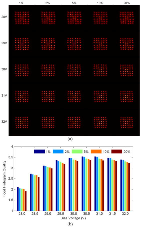
(a) flood histograms and (b) flood histogram quality versus bias voltage and capacitor tolerance.
Using capacitors with 0.2 nf value for n2, the flood histograms from the 1 mm pitch and the 0.7 mm pitch LSO crystal array are shown in Fig. 12(a) and (c). All crystals can be clearly identified. The unpolished 0.7 mm pitch LSO array was designed for a dual-ended readout DOI detector, resulting in significant depth-dependent light loss along the length of the crystal. Hence, a coincidence measurement was performed to irradiate the crystal at a fixed depth to mimic the dual-ended detector readout. Fig. 12(c) shows the flood histogram at a depth of 2 mm from the detector surface.
Fig. 12.
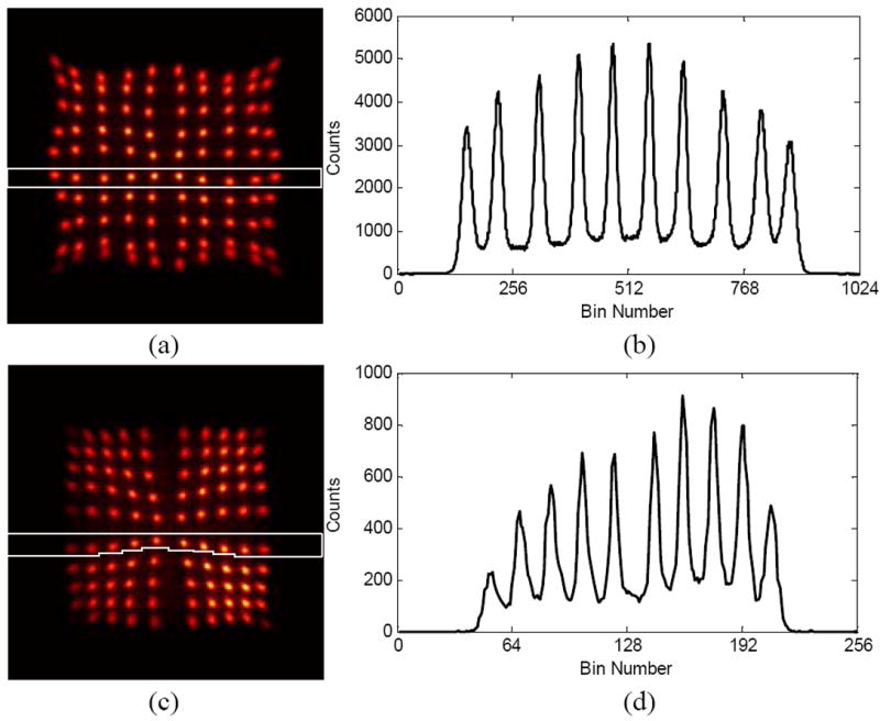
Flood histogram and position profile for ((a) and (b)) 1 mm pitch and ((c) and (d)) 0.7 mm pitch crystal array.
The position profiles for one crystal row (white rectangle in Fig. 12(a) and (c)) are plotted in Fig. 12(b) and (d). The average peak-to-valley ratios of the two position profiles are 7.3 and 5.5 respectively. Both the flood histograms and position profiles show the ability of the detector with capacitive charge sharing readout to resolve arrays with very small crystal elements.
E. Timing Resolution
The measured timing spectra using the 0.2 nf capacitors for n1 (corresponding n2 values are 0.4 nf) are shown in Fig. 13 (a) and the timing resolution using different capacitors are plotted in Fig. 13(b). In Fig. 13, the red and green curves indicate the results of using a 200 keV lower energy threshold and a 400 - 650 keV energy window, respectively. These energy filters were applied to each crystal individually. The blue and the black curves indicate the results with a crystal by crystal timing shift correction applied [18]. Better timing resolution was achieved using an energy window and timing shift calibration. The different capacitor values did not affect the timing resolution very much, especially when the timing shift calibration was used. A timing resolution of 8.8 ns was achieved using the 0.2 nf capacitors with timing shift calibration and a 400 – 650 keV energy window. The timing resolution is quite competitive with the gold standard of reading all 20 signals individually [4], which ranged from 6.8 ns (edge crystal) to 8.9 ns (center crystal).
Fig. 13.
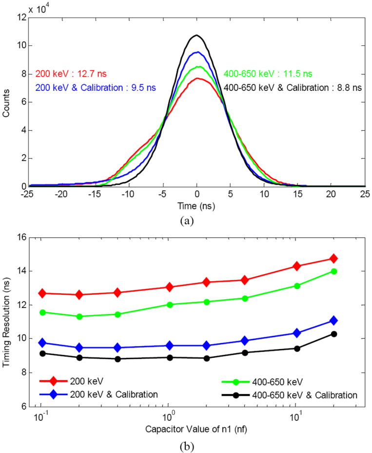
(a) Timing spectra using 0.2 nf capacitors and (b) timing resolution versus capacitor value.
IV. Conclusion and Discussion
In this study, a simple capacitive charge-division readout method for a 2 × 2 array of 5 mm × 5mm PS-SSPMs was developed and evaluated. Using this method only 5 electronic channels, instead of 20 channels, are needed to readout the 100 mm2 area of the 2 × 2 PS-SSPM array, dramatically reducing the number of readout channels and greatly simplifying the following electronics. Results from this thorough experimental evaluation show that better SNR, energy resolution, flood quality, and timing resolution, are achieved using capacitors with smaller values. However, there is a trade-off. Signal amplitudes are lower when using capacitors with smaller values, therefore a higher gain shaping circuit must accompany it. Because this detector technology is aimed at high spatial resolution applications, the flood histogram quality is a major consideration when evaluating the detector performance. The difference in flood histogram quality between capacitors with values of 0.051 nf, 0.1 nf, and 0.2 nf is minimal, therefore a capacitor value of 0.2 nf was chosen due to its overall performance characteristics. The capacitor tolerance does not significantly affect the noise, signal, and SNR, but does affect the energy resolution and flood histogram quality. Given the very large number of measurements presented in this manuscript, the results shown here are from individual datasets. Using subsets of the data to obtain multiple measurements for a small number of cases we found the uncertainty to be <0.5%. Errors from the fitting procedures also were very small as indicated in Figure 7. While a specific charge-sensitive preamplifier (Cremat CR-112) was used in this work, we anticipate that the same trends would hold for similar charge-sensitive preamplifiers, although the absolute values of the results may differ. Given the marginal price increase of capacitors with 1% or 2% tolerance, our conclusion is that the improvement gained in energy resolution and flood histogram quality makes the use of 1% or 2% tolerance capacitors advisable.
Compared to results obtained by reading all 20 signals individually [4] it is clear that the degradation caused by this multiplexing scheme is minimal. The best SNR measured in [4] is 29.9, while in this work a value of 24.4 was obtained. Timing resolution also was within the range (8.8 ns versus 6.8-8.9 ns for individual readout) previously measured. The reduction in the number of readout channels is significant, which is of major importance when contemplating a scanner based upon PS-SSPM detector technology as the scanner cost is influenced to number of electronic channels. A small animal PET system using a detector with scintillator pixelization of 0.7 mm should provide an image spatial resolution superior to any commercially available scanner. From the results shown we conclude that a multiplexed capacitor charge-sharing PS-SSPM array is capable of reading out such high spatial resolution scintillation arrays with good performance. For applications that do not require the use of such a finely pixelated scintillation array this method can also be easily used in a detector array containing more than four detectors, such as a 3 × 3 PS-SSPM array illustrated in Fig. 14. Although the proposed multiplexing method is presented for arrays of PS-SSPMs, in theory, it also can be applied to other position-sensitive detector arrays such as an array of PS-APDs.
Fig. 14.
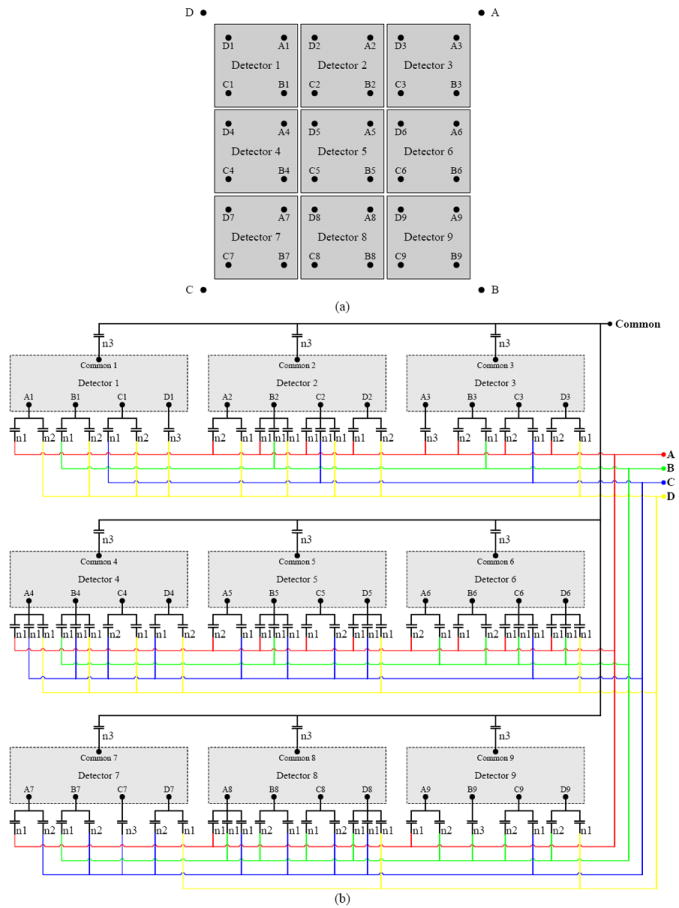
(a) Schematic of a 3 × 3 PS-SSPMs array and (b) schematic of the capacitive charge-division readout method for this 3 × 3 PS-SSPMs array.
Acknowledgments
This work was supported by NIH grant R01 CA134632.
Contributor Information
Junwei Du, Email: jwdu@ucdavis.edu, Department of Biomedical Engineering, University of California, Davis, CA 95616, USA.
Jeffrey P. Schmall, Department of Biomedical Engineering, University of California, Davis, CA 95616, USA.
Yongfeng Yang, Department of Biomedical Engineering, University of California, Davis, CA 95616, USA.
Kun Di, Department of Biomedical Engineering, University of California, Davis, CA 95616, USA.
Purushottam A. Dokhale, Radiation Monitoring Devices Inc., Watertown, MA 02172, USA
Kanai S. Shah, Radiation Monitoring Devices Inc., Watertown, MA 02172, USA
Simon R. Cherry, Department of Biomedical Engineering, University of California, Davis, CA 95616, USA.
References
- 1.McClish M, Dokhale P, Christian J, Stapels C, Johnson E, Robertson R, Shah KS. Performance measurements of CMOS position sensitive solid-state photomultipliers. IEEE Trans Nucl Sci. 2010 Aug;57(4):2280–2286. [Google Scholar]
- 2.Lewellen T. The challenge of detector designs for PET. Nuclear Medicine and Molecular Imaging. 2010 Aug;195(2):301–309. doi: 10.2214/AJR.10.4741. [DOI] [PubMed] [Google Scholar]
- 3.Roncali E, Cherry SR. Application of silicon photomultipliers to positron emission tomography. Annals of Biomedical Engineering. 2011 Apr;39(4):1358–1377. doi: 10.1007/s10439-011-0266-9. [DOI] [PMC free article] [PubMed] [Google Scholar]
- 4.Schmall J, Du J, Yang Y, Dokhale P, McClish M, Shah K, Cherry SR. Comparison of large-area position-sensitive solid-state photomultipliers for small animal PET. Phys Med Biol. 2012 Dec;57(24):8119–8134. doi: 10.1088/0031-9155/57/24/8119. [DOI] [PubMed] [Google Scholar]
- 5.Yang Y, Wu Y, Farrell R, Dokhale P, Shah K, Cherry SR. Signal and noise properties of position-sensitive avalanche photodiodes. Phys Med Biol. 2011 Oct;56(19):6327–6336. doi: 10.1088/0031-9155/56/19/011. [DOI] [PMC free article] [PubMed] [Google Scholar]
- 6.Siegel S, Silverman R, Shao Y, Cherry SR. Simple charge division readouts for imaging scintillator arrays using a multi-channel PMT. IEEE Trans Nucl Sci. 1996 Jun;43(3):1634–1641. [Google Scholar]
- 7.Doshi N, Silverman R, Shao Y, Cherry SR. maxPET: a dedicated mammary and axillary region PET imaging system for breast cancer. IEEE Trans Nucl Sci. 2001 Jun;48(3):811–815. [Google Scholar]
- 8.Popov V, Majewski S, Welch B. A novel readout concept for multianode photomultiplier tubes with pad matrix anode layout. Nucl Instrum Methods Phys Res A. 2006 Nov;567(1):319–322. [Google Scholar]
- 9.Wu Y, Catana C, Cherry SR. A multiplexer design for position- sensitive avalanche photodiode detector in a PET scanner. IEEE Trans Nucl Sci. 2008 Feb;55(1):463–468. [Google Scholar]
- 10.Lau F, Vandenbroucke A, Reynolds P, Olcott P, Horowitz M, Levin CS. Analog signal multiplexing for PSAPD-based PET detectors: simulation and experimental validation. Phys Med Biol. 2010 Dec;55(23):7149–7174. doi: 10.1088/0031-9155/55/23/001. [DOI] [PMC free article] [PubMed] [Google Scholar]
- 11.Song T, Wu H, Komarov S, Siegel S, Tai YC. A sub-millimeter resolution PET detector module using a multi-pixel photon counter array. Phys Med Biol. 2010 May;55(9):2573–2587. doi: 10.1088/0031-9155/55/9/010. [DOI] [PMC free article] [PubMed] [Google Scholar]
- 12.Shimizu K, Uchida H, Sakai K, Hirayanagi M, Nakamura S, Omura T. Development of an MPPC detector for PET. IEEE Nucl Sci Symp Med Imaging Conf Record. 2011:2991–2994. [Google Scholar]
- 13.Thompson C, Goertzen A. Evaluation of a 16:3 signal multiplexor to acquire signals from a SPM array with dual and single layer LYSO crystal blocks. IEEE Trans Nucl Sci. 2011 Oct;58(5):2175–2180. [Google Scholar]
- 14.Sens L. Matrix system user manual. 2012 May; Available: http://www.sensl.com.
- 15.Pullia A, Muller W, Boiano C, Bassini R. Resistive or capacitive charge-division readout for position-sensitive detectors. IEEE Trans Nucl Sci. 2002 Dec;49(6):3269–3277. [Google Scholar]
- 16.Kim E, Lee K, Park J. Signal splitting effect analysis for muon tracker signal in frequency domain. IEEE Nucl Sci Symp Med Imaging Conf Record. 2006;3:1322–1325. [Google Scholar]
- 17.Judenhofer M, Pichler B, Cherry SR. Evaluation of high performance data acquisition boards for simultaneous sampling of fast signals from PET detectors. Phys Med Biol. 2005 Jan;50(1):29–44. doi: 10.1088/0031-9155/50/1/003. [DOI] [PubMed] [Google Scholar]
- 18.Wu Y, Ng T, Yang Y, Shah K, Farrell R, Cherry SR. A study of the timing properties of position-sensitive avalanche photodiodes. Phys Med Biol. 2009 Aug;54(17):5155–5172. doi: 10.1088/0031-9155/54/17/006. [DOI] [PMC free article] [PubMed] [Google Scholar]
- 19.Peng H, Olcott P, Spanoudaki V, Levin CS. Investigation of a clinical PET detector module design that employs large-area avalanche photodetectors. Phys Med Biol. 2011 Jun;56(12):3603–3627. doi: 10.1088/0031-9155/56/12/010. [DOI] [PubMed] [Google Scholar]


