Abstract
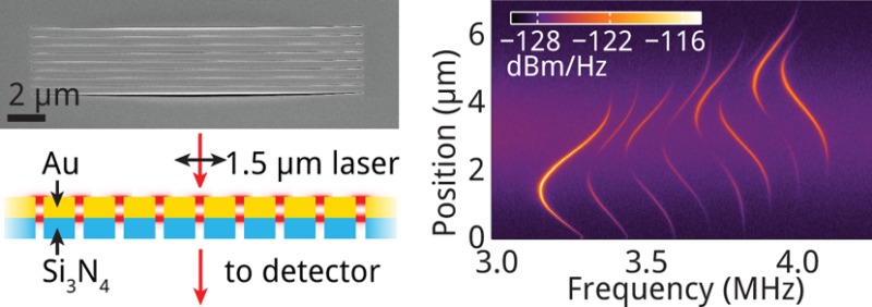
We demonstrate parallel transduction of thermally driven mechanical motion of an array of gold-coated silicon nitride nanomechanical beams, by using near-field confinement in plasmonic metal–insulator–metal resonators supported in the gap between the gold layers. The free-space optical readout, enabled by the plasmonic resonances, allows for addressing multiple mechanical resonators in a single measurement. Light absorbed in the metal layer of the beams modifies their mechanical properties, allowing photothermal tuning of the eigenfrequencies. The appearance of photothermally driven parametric amplification indicates the possibility of plasmonic mechanical actuation.
Keywords: plasmonics, optomechanics, near-field interactions, photothermal force, NEMS arrays, nano-optomechanical transducers
Arrays of nanomechanical resonators have many applications, ranging from force and mass sensing1,2 to collective nonlinear dynamics3 and mechanical memories and computing.4 In particular, large numbers of integrated mechanical sensors can enable sensitive, rapid, label-free, and massively parallel detection of biochemical species and trace gases.5,6 By varying the frequency of the oscillators in an array, the sensing bandwidth can be effectively increased. Parallelization can also address some of the difficulties associated with scaling down mechanical oscillator size, which is generally favorable for sensitivity: difficulties that include reduced power handling capability7,8 and reduced effective interaction cross section (i.e., the sensor surface area). Another challenge that nanoscale mechanical systems pose is how to efficiently transduce mechanical motion to a measurable signal, crucial to any sensor’s operation. In the case of a sensor consisting of multiple mechanical oscillators, it is often useful to create a system that can be measured using a single input and single output,9 by separating the oscillators in frequency. Mechanical arrays have been demonstrated using various readout schemes: electrical readout,10 using optical diffraction,11 and using (deformable) optical waveguides.12
Here, we demonstrate the parallel transduction of the motion of an array of nanobeams using a single laser beam focused on the array. The transduction is mediated by surface plasmon Fabry–Pérot resonances in the narrow metal-coated slots between the nanobeams. We show how this principle13,14 can be extended to measuring individual mechanical resonator modes in an array of nanobeams. We use metal–dielectric–metal plasmon resonances, which are very sensitive to the width of the dielectric region.15 Motion of the oscillator then changes the plasmonic configuration, thus changing the transmission of the cavity.
The small size of plasmonic resonators allows high mode overlap with nanomechanical modes. At the same time, the free-space addressability of localized surface plasmon resonances allows the use of simple optical elements to couple light to and from the cavity, without having to resort to for instance nanoscale positioning of waveguides, as is necessary for many photonic crystal cavity16 and microcavity17 optomechanical implementations. This free-space addressability makes measuring multiple mechanical oscillators with a single laser beam a relatively straightforward process.
During the measurement, the beams absorb some of the incident light. We demonstrate that this leads to photothermal modification of the beams’ eigenfrequencies.18−21 We discuss the induced mechanical coupling between the nanobeams. At high enough driving powers, the photothermal heating can parametrically amplify the motion of the beams. This photothermal amplification effect has been observed in a variety of optomechanical systems: in metal-coated cantilevers,22,23 in semiconductor membranes using electron–hole pair relaxation,24 and in microdisks.25 Photothermoelastic interactions may thus allow for both tuning and actuation in these systems.
Experimental Methods
To fabricate arrays of parallel mechanical nanobeams, 110 nm of gold is sputter coated on commercially available high-stress stoichiometric silicon nitride membranes of 50 nm thickness (Norcada, Canada). Using a focused ion beam (30 keV Ga+ ions, current 10 pA), we mill nine 18-μm-long slits in a single pass, creating eight nanomechanical beams, each separated by a slit width of 20 nm. The beam widths are fabricated to range in incrementing steps from 475 to 550 nm wide. The difference in beam widths lifts the degeneracy of the in-plane eigenfrequencies and allows the identification of individual beams from the transduced mechanical spectrum. The out-of-plane mechanical eigenfrequencies are to first order independent of beam width and are therefore more difficult to separate spectrally. However, the out-of-plane and in-plane eigenmodes are well separated in frequency (∼2.2 and ∼3.7 MHz, respectively), and we will mostly consider the latter below.
Figure 1a shows a scanning electron microscopy (SEM) image of the fabricated array, taken with the gold-coated side of the membrane upward and the sample tilted at 52°. The narrow gaps between the nanobeams are clearly visible; a larger gap is seen for the two outer sides, where the silicon nitride membrane bends downward due to its in-plane stress.
Figure 1.
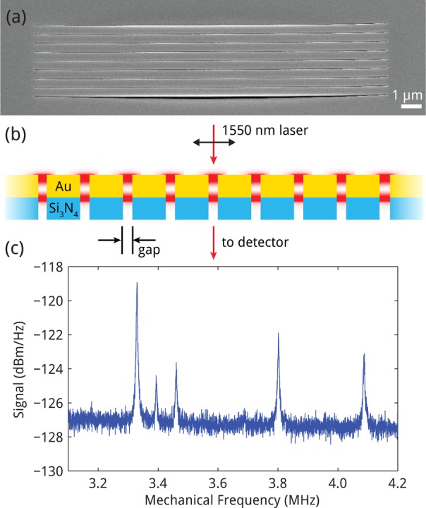
Experimental geometry. (a) SEM micrograph of array structure, tilted at 52°, taken on the gold side of an array of eight parallel microbeams (beam length: 18 μm; thickness: 50 nm Si3N4, 110 nm Au; beam widths: 475 to 550 nm; gap width: 20 nm). (b) Schematic cross section of the nanomechanical beam array. Red spots indicate plasmonic Fabry–Pérot resonances excited in the slits between the Au layers by a 1550 nm CW laser. (c) Frequency spectrum of light intensity transmitted through the array, showing five distinct resonances caused by five of eight nanomechanical beams in the array.
The sample is then placed in a custom-built confocal transmission microscope, which resides inside a vacuum chamber that is evacuated to 10–3 mbar to reduce viscous air drag on the nanobeams. A 1550 nm wavelength CW erbium-doped fiber laser is focused onto the sample, polarized orthogonal to the slits, and incident from the gold-coated side of the nanobeams, as shown in the schematic cross section in Figure 1b. Different focusing conditions were used, as will be described later on.
Nanomechanical Transduction
Mechanical displacement affects the optical response of the slots, changing the transmitted power. In the present geometry, the motion of eight parallel nanobeams is measured simultaneously. Figure 1c shows the frequency spectrum measured by defocusing the laser beam to a spot diameter of ∼5 μm, so that all plasmonic gaps are illuminated, and detecting a power of approximately 12 μW. The peaks are related to the thermal motion of individual mechanical modes. Interestingly, only five resonant mechanical modes are observed in the spectrum, with varying amplitude. To analyze this, we first discuss how the motion of the eight beams is transduced to the measured intensity.
The motion of each of the beams is probed by its two adjacent
slits,
each of which supports a plasmonic resonance. The transmitted power
through each slit can be written as η(di) , where
  is the
optical power density (in W/m2) interacting with slit i and η(d) is an effective scattering
cross section into the transmission
channel, which is a function of the slit width di.
For in-plane motion, the two slits
at either side of the beam have
widths d1(x) =  + x and d2(x) =
  – x, respectively,
where
  denotes the mean width of slit i, and x is the displacement of the beam
(we take the mean displacement x̅ = ⟨x(t)⟩ = 0). The total transmitted
power is, as such, T = η(
 + x)
+ x) + η(
+ η( – x)
– x) . This power is modulated through
oscillations
of the beam, as to first (linear) order
| 1 |
For a plane wave incident on a nanobeam surrounded
by two identical slits, this would lead to completely vanishing transduction
of motion as  and
and  . Figure 2a shows
a schematic of this geometry. An SEM image of such an array is shown
in Figure 2c. This equation can be expanded
to include the shape of the mechanical mode, by integrating along
the length of the beam, weighting the integral by the laser intensity
along the beam length. This will lead to a linear correction factor
for eq 1.
Figure 2.
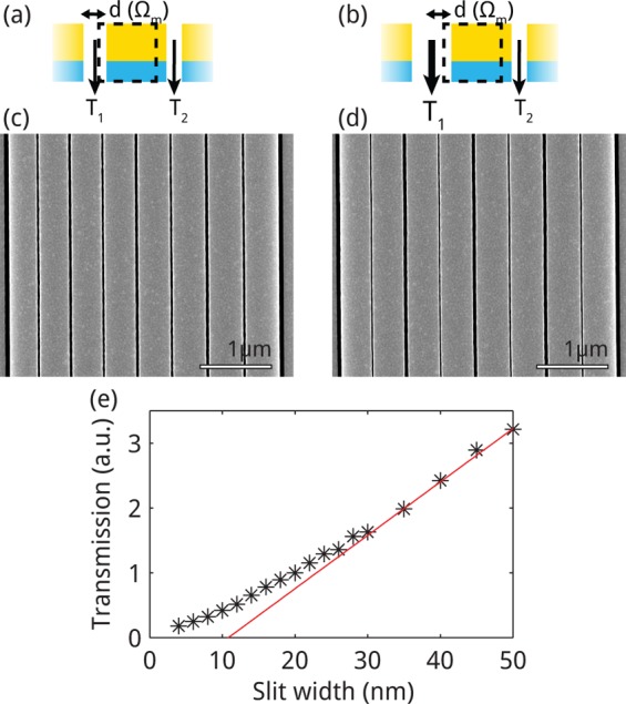
Parallel mechanical transduction. Schematic of transduction through (a) constant-width and (b) alternating-width gaps. SEM micrographs of center of arrays of (c) constant-width gap (20 nm) and (d) alternating-width gap (20 and 50 nm) array structures. (e) Transmission through slit as a function of slit width d, extracted from FDTD simulations. The red line is a linear fit to the transmission through slits of width greater than 35 nm.
So far, we considered only the slits immediately adjacent to the moving beam to contribute to transduction. While transduction through these two slits is likely dominating, it is in principle possible that the slits are optically coupled, leading to transduction involving other slits. We note that even for interacting slits the symmetry of the system and its illumination dictate that transduction vanishes for equal slit widths, if the total size of the array exceeds the typical coupling length. Assuming an array of slits, labeled from −i to i, the transmission through slit i is a function of the slit’s polarizability pi(x). With the incoming beam centered on the array, we have pi(x) = p–i(−x), if x denotes the in-plane displacement of the middle beam. This leads to a change in polarizability (d/dx)pi(x) = (d/dx)p–i(−x) = −(d/dx)p–i(x). The total transmitted field is then T ∝ ∑i∑jpipj*. Working out the terms in this equation for a modulation of the widths d–i, di of the center two slits leads to (dT/dx) = 0.
Two factors can potentially break down this expectation
and lead
to a resonance peak: (1) a different input power density  on the two
slits, due to the fact that
a nonuniform (for instance, a focused) beam is used, and (2) a difference
in slit widths
  . Because
the plasmonic coupling strength
depends on the slit width, η is not linearly dependent on d, such that (dη/dx)(
 ) ≠ (dη/dx)(
 ) if
) if  . This implies
that by changing the width
of the slit on either side of a beam we can allow transduction of
motion to transmitted power. Importantly, it is the nonlinear dependence
of slit transmission η on slit width d (or
on slit area, for that matter) that is crucial to allow transduction.
Such a nonlinear dependence on slit width, shown in Figure 2e, is a defining characteristic of plasmonic response.
In this figure, the black data points are the transmission extracted
from a series of FDTD simulations of slits of differing widths. The
transmission is normalized to the transmission through the 20-nm-wide
slit. The red line is a linear fit to slits of widths between 35 and
100 nm, showing the nonlinear behavior of the plasmonic transmission
for slit widths narrower than 30 nm.
In the structure of Figure 1 differences between slit widths are caused by fabrication imperfections, allowing observation of the motion of some of the beams in Figure 1c. The outermost slits in the structure are much wider: in-plane stress in the silicon nitride causes bending in the membrane surrounding the array structure, leading to a resonance peak for the two outermost beams. For some of the inner beams, the surrounding slits are also slightly different.
Next, we study the transduction
for an an array in which the slits
were intentionally made alternately narrow (20 nm) and wide (50 nm),
shown schematically in cross section in Figure 2b and in an SEM image in Figure 2d. For these
structures, we expect that (dη/dx)( ) ≠ (dη/dx)(
 ) for all beams, based on finite-difference-time-domain
simulations of metal–insulator–metal slits of varying
width (Figure 2e). Therefore, the motion of
all beams is expected to be transduced. At the laser wavelength of
1550 nm, we find from the FDTD simulations that (dη/dx)(20 nm) = 0.75(dη/dx)(50 nm).14
We again measured the transduction with a defocused beam and simultaneously detected the modulations induced by eight beams with widths ranging from 475 to 525 nm. This time, we achieve parallel transduction of motion of all eight beams, as shown in Figure 3, when we detect a power of 15 μW. Note that the signal-to-noise ratio is limited by the modest mechanical quality factor (typically Q < 1000) in this proof-of-principle demonstration. The mechanical quality factor can be straightforwardly improved by reducing the amount of gold near the beam ends.26 We have now seen that using alternate slit widths (20 and 50 nm) is a viable method to enable parallel transduction of the motion of eight parallel resonators using a single focused laser beam.
Figure 3.
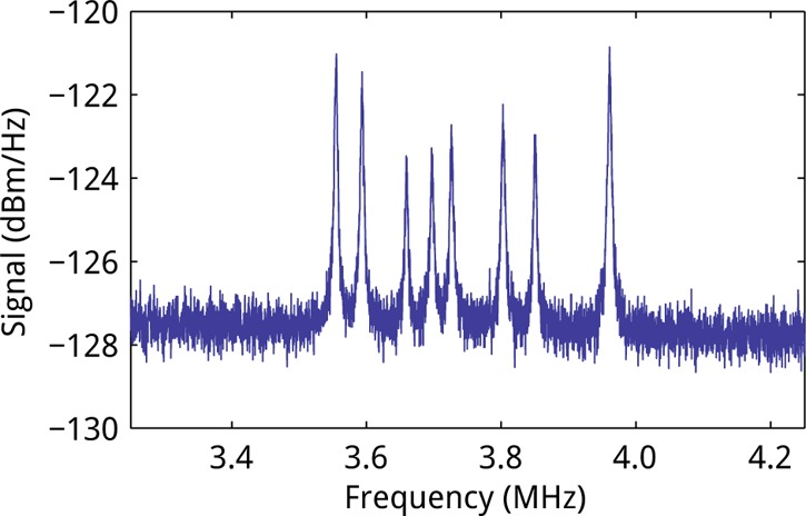
Frequency spectrum of light transmitted through an array with eight beams, with alternating-width slits of 20 and 50 nm, with beam widths ranging from 475 to 525 nm. The laser beam was defocused to a spot size of ∼5 μm.
To further investigate the transduction of each beam by its two neighboring slits, we perform measurements in which both structures were scanned through the focus of a laser beam (2.48 ± 0.06 μm fwhm for the constant-width array, 2.84 ± 0.13 μm for the alternating-width array), scanning orthogonal to the long axis of the beams. Figure 4a and b show color plots of the spectral density of transduced power as a function of the position of the laser beam across the constant-gap-width and alternate-gap-width arrays, respectively. Eight different curves are now clearly resolved for both structures, each corresponding to the motion of an individual nanobeam. Interestingly, as the laser beam is scanned across a single nanobeam, the mechanical resonance wavelength decreases and increases. This will be discussed further below.
Figure 4.
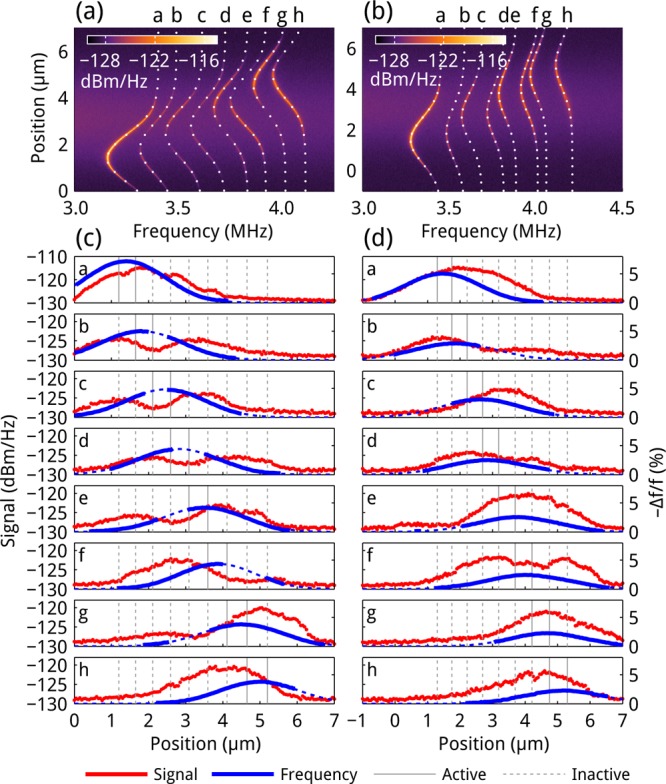
Mechanical resonance intensities. (a) Line scan across the center of an array of eight nanobeams separated by a fixed width of 20 nm. The peak resonance frequency is plotted on the horizontal axis, and the resonance peak intensity is represented by the color scale. Dots indicate Gaussian fits to peak frequencies as a function of the laser focus position on the array. (b) Similar to (a), for an array with beams alternately separated by 20 and 50 nm. (c) Transduction curves extracted from (a): the resonance peak intensities are shown as a function of laser spot position (red dots), along with the peak resonance frequencies (blue line). A dashed line indicates that the signal was too low to extract for use in fitting. The gray vertical lines indicate the positions of the slits, with the solid lines indicating the slits next to the beam for which the transduction is plotted. (d) Transduction curves extracted from (b). The focal diameters, 2.48 ± 0.06 μm fwhm for (a) and 2.84 ± 0.13 μm for (b), were determined from the average width of the Gaussian fits. Laser power detected was 11.5 μW (a, c) and 10.5 μW (b, d).
Another striking feature
in the transduction spectra in Figure 4a is
that the intensity shows clear dips close to
the center for all beams, except for the two outermost ones. The red
data points in the subpanels of Figure 4c show
the mechanical transduction power at resonance for each laser beam
position. Each subpanel shows data for a single beam. The transduction
curves clearly show dips in transduction for the six center beams
when the focal spot is close to the center of each beam, when  , implying a vanishing transduction, and
showing that d̅ is very similar for the seven
center slits. If the slits were all exactly equal in width, the shape
of the dip should be proportional to the derivative of the spatial
intensity profile of the laser spot on the sample. However, due to
fabrication imperfections, the slits have slightly differing widths.
We also attribute the transduction visible in Figure 1c to this. The mechanical transduction for each beam in the
alternate-gap-width array is plotted in Figure 4d. The dips in the transduction are now much less pronounced compared
to those observed for the constant-width array shown in Figure 4a and c and are in fact absent in most cases, showing
that (dη/dx)(50 nm) ≠ (dη/dx)(20 nm).
The measurements in Figures 3 and 4 provide direct proof that the transduction through the arrays is due to a plasmonic effect. If the transmission through the slits was simply due to a geometric effect, i.e., a transmission that is linearly proportional to the slit width, we would not observe any transduction of motion: for in-plane motion, the total width of the two slits surrounding a nanobeam is constant, and therefore no transduction would be expected. However, the plasmonic resonance mediating the transmission through the slit will lead to nonlinear dependence of transmission on slit width (as shown in Figure 2e), allowing the alternate-slit-width structure to improve transduction of the in-plane mechanical mode, and precludes the observed effects being due to a purely geometric modulation of the transmitted light by the beams’ motion.
Thermal Tuning of Eigenfrequencies
Figure 4 shows that the mechanical eigenfrequencies of the beams depend strongly on their position relative to the laser spot. We ascribe this to a photothermal effect: heating-induced expansion of the tensile-stressed beams causes a reduction in the axial stress, leading to reduced resonance frequencies. The maximum frequency shift is observed when the laser beam is centered on a nanobeam, where heating is maximum. We perform Gaussian fits to the (thermally shifted) resonance frequency as a function of laser focus position for each beam. The blue lines in the subpanels of Figure 4c and d show the thermally tuned frequency shift Δf = (ftuned – f0)/f0. Frequency shifts as high as 5% (150 kHz) are observed.
To further investigate this effect, we calculate the relative frequency shift as a function of absorbed power using a simple thermal model.18,19,20,21 We calculate the eigenfrequencies as a function of stress in the nitride layer of the beams:
| 2 |
with L the length of the beam, w the width, h the thickness, and I the geometrical moment of inertia, and using geometric averaging to calculate the effective stress σe, Young’s modulus Ee, and density ρe for the Au/Si3N4 bilayer beams.28,29 This geometric averaging is valid when most of the forces are along the length of the beams, implying that the system is far from buckling due to thermal stresses. As we are measuring the fundamental mode, we use β = 4.730 04.30 Note that all equations are also valid for single-layer beams.
To fit the model to the data, we first extract the nonthermally shifted eigenfrequencies fi from the Gaussian fits in Figure 4a,b and plot these as a function of beam width in Figure 5a. We then fit eq 2 to the data using the effective Young’s modulus Ee and stress σe as free parameters, using length and height as determined from SEM images and using literature values for the mass densities of gold and silicon nitride. Figure 5a shows good agreement between model and data for an effective Young’s modulus of Ee = 75.2 GPa, between the value of that for gold and silicon nitride. We will assume the Young’s moduli are independent of temperature.31,32 The fitted effective stress (in the low-power limit) is 36.5 MPa. Assuming the manufacturer’s specification of σe = 250 MPa, this implies that there is a compressive stress of σAu = −60 MPa in the gold layer.
Figure 5.
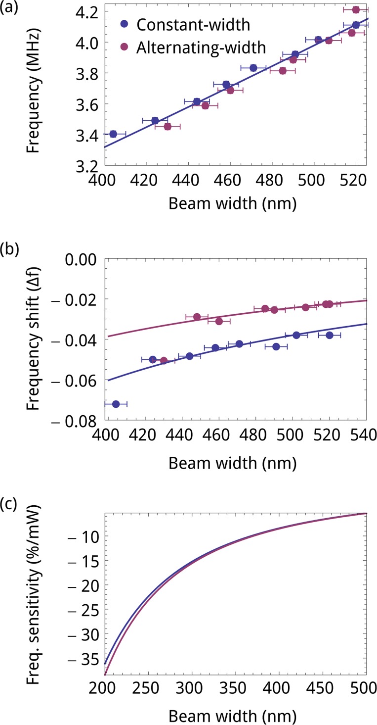
(a) Nonthermally shifted eigenfrequencies for constant-width array (blue data points derived from Figure 4a,c) and alternate-width array (red dots, derived from Figure 4b,d) and model, fitting effective Young’s modulus Ee and in-plane stress σe. (b) Measured thermally induced maximum frequency shifts from Figure 4 for constant-width (blue) and alternating-width (red) arrays as a function of beam width. The drawn lines are fits using eq 6, with the fraction of absorbed power γ as a free parameter. (c) Calculated frequency shift in %/mW of absorbed power for a gold-coated silicon nitride beam, plotted as a function of beam width. The purple line is for the alternating-width array; the blue line, for the constant-width array.
Next, we investigate the effect of heating of the nanobeams as they absorb light, changing the stress in the nanobeam through the thermal expansion coefficient:
| 3 |
where σi is the original stress determined above, σt is the thermal stress, ΔT is the average temperature increase of the nanobeam, and αe is the effective thermal expansion coefficient αe = (αSi3N4ASi3N4 + αAuAAu)/(ASi3N4 + AAu),where Ai = wi × hi is the cross-sectional area of layer i. For this formulation for σe to be valid, we assume the end points of the beam do not move. We can then calculate the relative frequency change due to heating, using eq 2:
| 4 |
where ft is the thermally tuned frequency (eq 2 with σ from eq 3), fi is the prestressed frequency without heating (eq 2 with σe = σi), and f0 is the eigenfrequency for a beam with no added stress (σe = 0).
We use a one-dimensional heating model, in which the beam is heated by a power Pabs applied evenly across the cross section of the beam at x0, while the ends of the beam are kept at ambient temperature (T(0) = T(L) = 298 K). In the stationary case, the absorbed power equals the outgoing fluxes:
| 5 |
with κ the heat conductivity, so that ΔT = PabsL/8κA. Using eqs 3–5, we find
| 6 |
The untuned frequencies f0 and fi are extracted from the Gaussian fits to the thermal tuning as shown in Figures 4 and 5a. Effective parameters for α and κ are derived from the weighted averages using αSi3N4 = 1.23 × 10⁻⁶ K–1, αAu = 14 × 10–6 K–1, κSi3N4 = 2.5 W m–1 K–1, and κAu = 320 W m–1 K–1.20 That leaves the absorbed power Pabs to be directly determined from δf using eq 6.
Assuming the laser focus has a 2D Gaussian shape, the power density absorbed on one beam, with width w, can be expressed as a function of the incident power Pin and a parameter γ describing the fraction of incident power that is absorbed in the beam:
| 7 |
For example, for the constant-width array, a 500-nm-wide beam has 18% of the total optical power incident upon it, given the laser spot size. For the alternating-width array, the slightly larger focal width leads to a 500-nm-wide beam having 16% of the total power incident upon it. Figure 5b shows the measured maximum thermally induced frequency shift from Figure 4 as a function of beam width for the constant-width and alternating-width arrays. The frequency shift is stronger for narrower beams, as these have a lower heat capacity. The drawn lines are fits of eq 6 to the data, taking into account the width dependence of the incident power on the area of the beam (eq 7) and assuming a fixed fraction γ of the power incident on the beam to be absorbed in the beam. We find the data can be fitted well with this model for both constant- and alternating-width arrays and find that for a 500-nm-wide beam Pabs = 611 μW for the constant-width array and Pabs = 396 μW for the alternating-width array.
Using the thermal frequency shift model, we find that for both the constant-width and alternating-width arrays, the sensitivity of frequency to absorbed power is, for a 500-nm-wide beam, δf/Pabs = 6%/mW. This is shown in Figure 5c, dividing out the focal width and power in Figure 5b. Because the heat capacity of a narrow beam scales with its width, the narrower beams are more sensitive to Pabs. We find that the sensitivity to absorbed power is the same for both structures, as would be expected.
Parametric Oscillation of Nanobeams
We have also studied the out-of-plane mechanical mode under high illumination power; Figure 6 shows the mechanical resonance spectrum for an array of eight beams under 10 mW irradiation. The mechanical transduction amplitude exceeds the noise by 50 dB and is much more than in Figure 3. Also, the effective quality factor of the resonance increases to Qm > 50.000; this is a lower limit determined by thermal fluctuations that shift the resonance during the measurement averaging time. Figure 6 shows several harmonics at a frequency spacing exactly equal to the fundamental frequency of 2.21 MHz. The appearance of these higher order sidebands is intrinsic to the large modulation amplitude (up to 10% of the dc transmitted power). At these modulation amplitudes, power is transferred not only to the first sideband but also to higher order sidebands.33 Spectra such as that shown in Figure 6 are observed for laser powers > 8 mW, with the exact threshold depending on the laser focusing condition.
Figure 6.
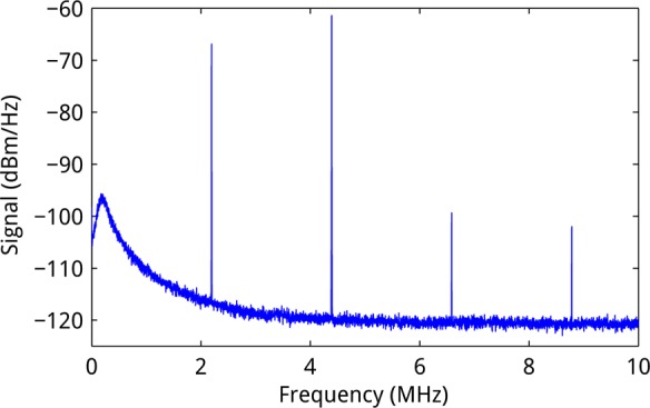
Mechanical response of a beam undergoing thermally induced parametric amplification, showing greatly increased response amplitude, high effective Q-factor, and higher order sidebands of the fundamental out-of-plane mode at 2.21 MHz.
We attribute this behavior to parametric oscillations17,21 that occur due to a driving force that is bolometric in nature:25,34 for the out-of-plane mode, power absorbed in the beams causes an out-of-plane bending stress, due to the bilayer geometry of the beams and the differing thermal expansion coefficients αSi3N4 and αAu of silicon nitride and gold, which, if this stress is modulated at twice the mechanical frequency, can lead to parametric oscillations. When the out-of-plane displacement of one of the beams increases, the incoupling into the plasmonic resonance is reduced, reducing the heating and allowing the beam to cool off, with a certain time delay controlled by the heat capacity, restoring the equilibrium position. Then, light can be coupled back into the cavity, once again increasing absorption, driving the beams to greater and greater displacement. This process is eventually limited by coupling of mechanical energy into the higher harmonics of the system.
Avoided Crossings in Arrays of Beams
Multiple mechanical oscillators can not only be used for parallelization of measurements. If the mechanical modes are coupled, a range of different effects can be observed and exploited, for instance using localized modes35 to improve sensitivity36 or using coupled resonances to create mechanical RF filters,37,38 to enable single-input single-output mass sensing39 or to observe synchronization.40
If two resonators are coupled and then are tuned to make their eigenfrequencies match, their eigenfrequencies as a function of coupling will show an avoided crossing, as shown earlier for nanomechanical systems.41,42 Figure 7b shows a FEM simulation of the in-plane eigenmode of the fourth beam, showing that the neighboring beams also contribute to the eigenmode. To study the coupling between the beams, we fabricated an array of eight beams with beam widths leading to in-plane eigenfrequencies such that they could be thermally tuned to match. This was achieved by fabricating an array of eight beams with widths of 425, 450, 459, 480, 500, 525, 545, and 570 nm, where the second and third beams have nearly identical widths. The gap widths were fabricated to be alternating between 20 and 40 nm.
Figure 7.
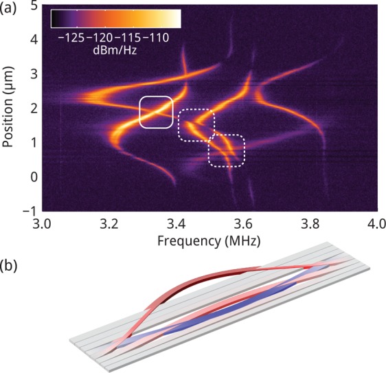
(a) Mechanical transduction spectrum of an array of eight microbeams, engineered to show avoided crossings in the thermally tuned eigenfrequencies of the microbeams. The widths of the beams were chosen such that one pair of neighboring beams would have similar eigenfrequencies. The dashed outlines indicate avoided crossings. The solid outline indicates a nonavoided crossing. (b) Simulated array of beams of increasing widths showing the shape of the fourth in-plane eigenmode, showing that the neighboring beams are also in motion due to the coupling at the anchoring points of the beams. Displacements are greatly exaggerated for clarity.
Figure 7a shows the measured mechanical transduction as a function of frequency and of the position of the focused laser beam in the array. The thermal tuning behavior observed in Figure 4 is clearly observed for four beams. Two avoided crossings are observed, indicated by the dashed outlines.
We also observe a nonavoided crossing, suggesting these mechanical modes are related to nonadjacent beams. For nonadjacent beams, we expect very low mechanical coupling between these beams and, therefore, do not expect to see a splitting in the crossing.
Conclusion
We demonstrate parallel transduction of the thermally driven mechanical motion of an array of nanobeams using a simple free-space technique. The motion of each beam is transduced by the adjacent plasmonic slits. When these are identical, the transduction of in-plane motion can cancel, due to antisymmetric transduction by the slits. By tuning the gap width, the plasmonic resonances are tuned, allowing simultaneous parallel transduction of the mechanical modes of all beams.
The thermal tuning due to optical power absorption leads to resonance frequency shifts as large as 6%/mW of power absorbed in the beam. At powers above 8 mW parametric oscillations are observed due to a bolometric driving force. We find that neighboring beams are mechanically coupled through the membrane in which they are suspended. When thermally tuning such an array to make the eigenfrequencies of two neighboring beams match, the coupling between these beams creates an avoided crossing in the transduced mechanical modes of these two beams. The photothermoelastic effect observed in this work could therefore find application in tuning and actuating plasmonic micro- and nanomechanical resonators.
The principle of parallel plasmonic mechanical transduction could be used in a variety of sensor array applications, due to its simple free-space readout and scalability to include many more resonators than shown here.
Acknowledgments
This work is part of the research program of the “Stichting voor Fundamenteel Onderzoek der Materie” (FOM), which is financially supported by the “Nederlandse Organisatie voor Wetenschappelijk Onderzoek” (NWO). This work is also supported by the European Research Council.
The authors declare no competing financial interest.
References
- Ekinci K. L.; Roukes M. L. Nanoelectromechanical systems. Rev. Sci. Instrum. 2005, 76, 061101. [Google Scholar]
- Li M.; Tang H. X.; Roukes M. L. Ultra-sensitive NEMS-based cantilevers for sensing, scanned probe and very high-frequency applications. Nat. Nanotechnol. 2007, 2, 114–120. [DOI] [PubMed] [Google Scholar]
- Lifshitz R.; Kenig E.; Cross M. C. Collective dynamics in arrays of coupled nonlinear resonators. In Fluctuating Nonlinear Oscillators; Dykman M. I., Ed.; Oxford University Press, 2012; Chapter 11. [Google Scholar]
- Mahboob I.; Mounaix M.; Nishiguchi K.; Fujiwara A.; Yamaguchi H. A multimode electromechanical parametric resonator array. Sci. Rep. 2014, 4, 4448. [DOI] [PMC free article] [PubMed] [Google Scholar]
- Waggoner P. S.; Craighead H. G. Micro- and nanomechanical sensors for environmental, chemical, and biological detection. Lab Chip 2007, 7, 1238–1255. [DOI] [PubMed] [Google Scholar]
- Datar R.; Kim S.; Jeon S.; Hesketh P.; Manalis S.; Boisen A.; Thundat T. Cantilever sensors: nanomechanical tools for diagnostics. MRS Bull. 2009, 34, 449–454. [Google Scholar]
- Arlett J. L.; Myers E. B.; Roukes M. L. Comparative advantages of mechanical biosensors. Nat. Nanotechnol. 2011, 6, 203–215. [DOI] [PMC free article] [PubMed] [Google Scholar]
- Bargatin I.; Myers E. B.; Aldridge J. S.; Marcoux C.; Brianceau P.; Duraffourg L.; Colinet E.; Hentz S.; Andreucci P.; Roukes M. L. Large-scale integration of nanoelectromechanical systems for gas sensing applications. Nano Lett. 2012, 12, 1269–1274. [DOI] [PMC free article] [PubMed] [Google Scholar]
- Sadek A. S.; Karabalin R. B.; Du J.; Roukes M. L.; Koch C.; Masmanidis S. C. Wiring nanoscale biosensors with piezoelectric nanomechanical resonators. Nano Lett. 2010, 10, 1769–1773. [DOI] [PubMed] [Google Scholar]
- Truitt P. A.; Hertzberg J. B.; Huang C. C.; Ekinci K. L.; Schwab K. C. Efficient and sensitive capacitive readout of nanomechanical resonator arrays. Nano Lett. 2007, 7, 120–126. [DOI] [PubMed] [Google Scholar]
- Yue M.; Stachowiak J. C.; Lin H.; Datar R.; Cote R.; Majumdar A.. Label-free protein recognition two-dimensional array using nanomechanical sensors. Nano Lett. 2008, 8, 520–524. [DOI] [PubMed] [Google Scholar]
- Li M.; Pernice W. H. P.; Tang H. X. Broadband all-photonic transduction of nanocantilevers. Nat. Nanotechnol. 2009, 4, 377–382. [DOI] [PubMed] [Google Scholar]
- Ou J.-Y.; Plum E.; Zhang J.; Zheludev N. I. An electromechanically reconfigurable plasmonic metamaterial operating in the near-infrared. Nat. Nanotechnol. 2013, 8, 252–255. [DOI] [PubMed] [Google Scholar]
- Thijssen R.; Verhagen E.; Kippenberg T. J.; Polman A.. Plasmon nanomechanical coupling for nanoscale transduction. Nano Lett. 2013, 13, 3293–3297. [DOI] [PubMed] [Google Scholar]
- Miyazaki H. T.; Kurokawa Y. Squeezing visible light waves into a 3-nm-thick and 55-nm-long plasmon cavity. Phys. Rev. Lett. 2006, 96, 097401. [DOI] [PubMed] [Google Scholar]
- Eichenfield M.; Camacho R.; Chan J.; Vahala K. J.; Painter O. A picogram- and nanometre-scale photonic-crystal optomechanical cavity. Nature 2009, 459, 550–555. [DOI] [PubMed] [Google Scholar]
- Kippenberg T. J.; Rokhsari H.; Carmon T.; Scherer A.; Vahala K. J. Analysis of radiation-pressure induced mechanical oscillation of an optical microcavity. Phys. Rev. Lett. 2005, 95, 033901. [DOI] [PubMed] [Google Scholar]
- Jun S. C.; Huang X. M. H.; Manolidis M.; Zorman C. A.; Mehregany M.; Hone J. Electrothermal tuning of Al-SiC nanomechanical resonators. Nanotechnology 2006, 17, 1506. [Google Scholar]
- Larsen T.; Schmid S.; Villanueva L. G.; Boisen A. Photothermal analysis of individual nanoparticulate samples using micromechanical resonators. ACS Nano 2013, 7, 6188–6193. [DOI] [PubMed] [Google Scholar]
- Schmid S.; Wu K.; Larsen P. E.; Rindzevicius T.; Boisen A. Low-power photothermal probing of single plasmonic nanostructures with nanomechanical string resonators. Nano Lett. 2014, 14, 2318–2321. [DOI] [PubMed] [Google Scholar]
- Yamada S.; Schmid S.; Larsen T.; Hansen O.; Boisen A. Photothermal infrared spectroscopy of airborne samples with mechanical string resonators. Anal. Chem. 2013, 85, 10531–10535. [DOI] [PubMed] [Google Scholar]
- Metzger C. H.; Karrai K. Cavity cooling of a microlever. Nature 2004, 432, 1002–1005. [DOI] [PubMed] [Google Scholar]
- Holscher P. H; Milde; Zerweck U.; Eng L. M.; Hoffmann R. The effective quality factor at low temperatures in dynamic force microscopes with Fabry-Pérot interferometer detection. Appl. Phys. Lett. 2009, 94, 223514. [Google Scholar]
- Usami K.; Naesby A.; Bagci T.; Nielsen B. M.; Liu J.; Stobbe S.; Lodahl P.; Polzik E. S. Optical cavity cooling of mechanical modes of a semiconductor nanomembrane. Nat. Phys. 2012, 8, 168. [Google Scholar]
- Zalalutdinov M.; Zehnder A.; Olkhovets A.; Turner S.; Sekaric L.; Ilic D. B.; Czaplewski; Parpia J. M.; Craighead H. G. Autoparametric optical drive for micromechanical oscillators. Appl. Phys. Lett. 2001, 79, 695. [Google Scholar]
- Schmid S.; Jensen K. D.; Nielsen K. H.; Boisen A. Damping mechanisms in high-Q micro and nanomechanical string resonators. Phys. Rev. B 2011, 84, 165307. [Google Scholar]
- Su Y.-J.; Qian C.-F.; Zhao M.-H.; Zhang T.-Y. Microbridge testing of silicon oxide/silicon nitride bilayer films deposited on silicon wafers. Acta Mater. 2000, 48, 4901–4915. [Google Scholar]
- Bose S.; Schmid S.; Larsen T.; Keller S. S.; Sommer-Larsen P.; Boisen A.; Almdal K. Micromechanical string resonators: analytical tool for thermal characterization of polymers. ACS Macro Lett. 2014, 3, 55–58. [DOI] [PubMed] [Google Scholar]
- Weaver W.; Timoshenko S.; Young D.. Vibration Problems in Engineering; John Wiley & Sons, 1990. [Google Scholar]
- Chang Y. A.; Himmel L. Temperature dependence of the elastic constants of Cu, Ag, and Au above room temperature. J. Appl. Phys. 1966, 37, 3567–3572. [Google Scholar]
- Rouxel T.; Sanglebœuf J.-C.; Huger M.; Gault C.; Besson J.-L.; Testu S. Temperature dependence of Young’s modulus in Si3N4-based ceramics: roles of sintering additives and of SiC-particle content. Acta Mater. 2002, 50, 1669–1682. [Google Scholar]
- Schliesser A.; Riviere R.; Anetsberger G.; Arcizet O.; Kippenberg T. J. Resolved-sideband cooling of a micromechanical oscillator. Nat. Phys. 2008, 4, 415–419. [Google Scholar]
- Metzger C.; Ludwig M.; Neuenhahn C.; Ortlieb A.; Favero I.; Karrai K.; Marquardt F. Self-induced oscillations in an optomechanical system driven by bolometric backaction. Phys. Rev. Lett. 2008, 101, 133903. [DOI] [PubMed] [Google Scholar]
- Sato M.; Hubbard B. E.; Sievers A. J.; Ilic B.; Czaplewski D. A.; Craighead H. G. Observation of locked intrinsic localized vibrational modes in a micromechanical oscillator array. Phys. Rev. Lett. 2003, 90, 044102. [DOI] [PubMed] [Google Scholar]
- Spletzer M.; Raman A.; Sumali H.; Sullivan J. P. Highly sensitive mass detection and identification using vibration localization in coupled microcantilever arrays. Appl. Phys. Lett. 2008, 92, 114102. [Google Scholar]
- Galayko D.; Kaiser A.; Legrand B.; Buchaillot L.; Combi C.; Collard D. Coupled-resonator micromechanical filters with voltage tuneable bandpass characteristic in thick-film polysilicon technology. Sens. Actuators, A 2006, 126, 227–240. [Google Scholar]
- Nguyen C.-C. MEMS technology for timing and frequency control. IEEE Trans. Ultrason., Ferroelectr., Freq. Control 2007, 54, 251–270. [DOI] [PubMed] [Google Scholar]
- DeMartini B. E.; Rhoads J. F.; Zielke M. A.; Owen K. G.; Shaw S. W.; Turner K. L. A single input-single output coupled microresonator array for the detection and identification of multiple analytes. Appl. Phys. Lett. 2008, 93, 054102. [Google Scholar]
- Shim S.-B.; Imboden M.; Mohanty P. Synchronized oscillation in coupled nanomechanical oscillators. Science 2007, 316, 95–99. [DOI] [PubMed] [Google Scholar]
- Buks E.; Roukes M. L. Electrically tunable collective response in a coupled micromechanical array. J. Microelectromech. Syst. 2002, 11, 802–807. [Google Scholar]
- Okamoto H.; Gourgout A.; Chang C.-Y.; Onomitsu K.; Mahboob I.; Chang E. Y.; Yamaguchi H. Coherent phonon manipulation in coupled mechanical resonators. Nat. Phys. 2013, 9, 480–484. [Google Scholar]


