Abstract
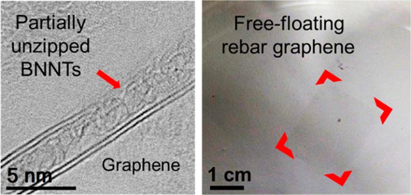
The synthesis of rebar graphene on Cu substrates is described using functionalized boron nitride nanotubes (BNNTs) that were annealed or subjected to chemical vapor deposition (CVD) growth of graphene. Characterization shows that the BNNTs partially unzip and form a reinforcing bar (rebar) network within the graphene layer that enhances the mechanical strength through covalent bonds. The rebar graphene is transferrable to other substrates without polymer assistance. The optical transmittance and conductivity of the hybrid rebar graphene film was tested, and a field effect transistor was fabricated to explore its electrical properties. This method of synthesizing 2D hybrid graphene/BN structures should enable the hybridization of various 1D nanotube and 2D layered structures with enhanced mechanical properties.
Keywords: rebar graphene, BNNTs, free-standing, BCN hybrid structure, CVD, STEM
Graphene, an important member in the family of carbon nanomaterials, has drawn enormous attention since its discovery.1,2 With a conjugated hexagonal structure of carbon atoms, graphene has shown outstanding properties in mechanical strength, optical transparency and electronic and thermal conductivity, which leads to interest in fields such as electronics for transparent conductive electrodes,3,4 and field effect transistors (FETs).5,6 A 1:1 mixture of boron and nitrogen (boron nitride, BN) is isoelectronic to carbon and can also form hexagonal low dimensional nanomaterials including 2D h-BN and 1D BN nanotubes (BNNTs), which share an atomic structure similar to graphene and carbon nanotubes (CNTs).7,8 The BN nanomaterials are similar to or more transparent, thermally stable, and thermally conductive than carbon nanomaterials, yet 2D h-BN is insulating with a bandgap up to 5.9 eV.9
Due to having similar hexagonal structures, B–N and C–C bonds tend to segregate in BCN systems.10 Much research has been directed to the study of hybridized hexagonal BCN structures as they provide a new approach to tailor the physical and chemical properties of 2D nanomaterials.11−15 Interesting applications include high-performance oxygen reduction reaction (ORR) catalysts,14 bandgap modifications of BN-doped graphene,13,16 and as active layers in FETs.15 However, current studies of BCN structures have been limited to the hybridization between 2D graphene and 2D h-BN, or doping of carbon/BN nanomaterials by B, N or C atoms; yet the hybridization between 2D graphene and 1D BNNTs remains unstudied.
Recently, our group reported the synthesis of a 2D hybrid structure of 2D graphene and 1D CNTs, called rebar graphene, via an annealing and growth protocol that produces graphene with enhanced mechanical strength due to the reinforcement effect of the CNTs.17 Characterization showed that the CNTs were partially unzipped and merged into the graphene layer to generate covalent connections between the two materials. Similarly, taking advantage of this concept of rebar graphene and the shared hexagonal structure of BNNTs and graphene, here we report a 2D hybrid BCN structure of 2D graphene and 1D BNNTs, namely rebar graphene with BNNTs. This rebar film was synthesized from functionalized or wrapped BNNTs, where the covalent bonding between partially unzipped BNNTs and graphene enhanced the mechanical strength of the 2D sheet enabling transfer of the sheet to another substrate without polymer adhesion.
Results and Discussion
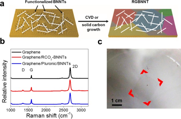
The synthesis scheme of the rebar graphene with BNNTs (RGBNNT) is shown in Figure 1a. Highly crystalline, long, few-walled BNNTs synthesized by a catalyst-free high temperature pressure (HTP) laser heating method (Supporting Information Figure S1) were used as starting materials.18 Functionalized BNNT solutions were prepared using two approaches. In the first approach, 2-ethylhexanoyl functionalized-BNNTs (RCO2–BNNTs) were prepared by sonicating BNNTs with HNO3 to introduce hydroxyl groups (HO-BNNTs),19 followed by reaction with 2-ethylhexanoyl chloride for 120 h to form the 2-ethylhexanoyl esters.20 Surfactant (Pluronic F127) dispersed BNNTs (Pluronic/BNNTs) were prepared by tip-sonicating BNNTs with Pluronic F127 solution for 1 min. Digital photos of the functionalized BNNT solutions and TEM images of single RCO2–BNNT and Pluronic/BNNT tubes are shown in Supporting Information Figure S2. The functionalized BNNT solutions (0.2 mg/mL) were spin-coated onto pretreated Cu foils (1 cm × 1 cm).21 The synthesis of rebar graphene was then performed in a tubular furnace with and without CH4 as the carbon source. When using CH4 as the carbon source, the Cu foils were loaded into a CVD furnace at 1077 °C, annealed with 500 sccm H2 at 7 Torr for 5 min, and then an additional 1 sccm CH4 was introduced for 15 min. When not using CH4 as the carbon source, the Cu foils were loaded into a furnace at 1077 °C, and then annealed with 500 sccm Ar and 50 sccm H2 at 7 Torr for 20 min. In this case, the RCO2-functional groups or the wrapped Pluronic surfactant served as the carbon sources for the graphene growth. Experimental details are included in the Supporting Information. To simplify, the synthesis of RGBNNT using RCO2–BNNTs and CH4 is denoted as method 1; the synthesis of RGBNNT using RCO2–BNNTs without CH4 is denoted method 2; the synthesis of RGBNNT with Pluronic/BNNTs with CH4 is denoted as method 3; and the synthesis of RGBNNT with Pluronic/BNNTs without CH4 is denoted as method 4. All growth methods afforded nearly identical 2D-film products.
Figure 1.
(a) The synthesis of RGBNNT was accomplished by first depositing functionalized BNNTs onto Cu foil, and then conducting the CVD or solid carbon source process for graphene growth. (b) Raman spectra (excited with 514 nm laser) of as-grown RGBNNT on a SiO2/Si substrate, showing that single-layer graphene sheets were synthesized using method 1 and method 3. (c) Photograph of free-floating RGBNNT synthesized using method 1. Red highlights are used to enhance visualization of the high-transparency rectangular film.
To investigate the formation of graphene after annealing or CVD growth, Raman spectra were taken of the product on the Cu foils (Supporting Information Figure S3). For all four methods, the representative Raman spectra show a G band at ∼1585 cm–1 and a 2D band at ∼2690 cm–1, similar to those of graphene synthesized using the CVD reaction with CH4 as the carbon source but without any BNNTs. As the ratio between the intensity of the 2D band and the G band in Raman spectra has been widely used to determine the number of layers of graphene,22,23 the as-grown RGBNNT was found to be single-layer graphene with a 2D/G intensity ratio of ∼3, similar to that from rebar graphene made using CNTs.17
Interestingly, while an external gas flow (CH4 for instance) is often used as the primary carbon source for graphene growth,24 here monolayer graphene was also synthesized without introducing CH4 (method 2 and method 4), as shown in Supporting Information Figure S3. In this case, the RCO2–BNNTs functional groups or the Pluronic surfactant in the Pluronic/BNNTs were alternative carbon sources for graphene growth.17 This CH4-free approach, similar to the use of solid carbon sources for graphene growth,25−28 provides another method for the synthesis of RGBNNT.
To eliminate the influence of Cu fluorescence and obtain better resolution for the Raman analyses, the synthesized RGBNNT and graphene produced without BNNTs were transferred onto SiO2/Si substrates followed by Raman analyses. From Figure 1b, compared to the control (single-layer graphene), the RGBNNT made from method 1 and method 3 both showed weak but higher D band (∼1345 cm–1) and D′ band (∼1620 cm–1, shoulder peak) signal, which originate from the distortion in the graphene lattice.29 In addition, from the Raman mapping data shown in Supporting Information Figure S4, RGBNNT made from all four methods show higher D/G ratios in a 100 μm2 area when compared with single-layer graphene, yet with a relatively constant range for 2D/G ratios. These increased distortion peaks within RGBNNT were caused by graphene/BN hybridization,13,15 yet the single-layer characteristic of graphene is well-retained. Although the distribution of the D/G ratio is not perfectly uniform throughout the mapped area, this variation is probably not a good correlation with the position of the BNNTs, as the size of BNNTs, with a diameter of 5 to 10 nm, is much smaller than the size of the Raman laser spot, with a diameter of 1 to 2 μm. The Raman spectra of spin-coated BNNTs on Cu foils are shown in Supporting Information Figure S5, with a weak peak at ∼1370 cm–1, corresponding to the hexagonal BN structure.30,31 After graphene growth, however, these weak peaks were no longer observed (Figure 1b, Supporting Figure S5), indicating the damage of the BNNT structure, as induced by the interaction between graphene and BNNTs which share the hexagonal structure.
For most conventional methods, the use of a polymer to assist transfer is required when graphene32,33 or graphene-like 2D materials34,35 are transferred onto other substrates after growth. To test the mechanical strength and ability to transfer without assistance from a polymer, the RGBNNT on Cu foil (method 1) was etched in (NH4)2S2O8/H2O/C4H9OH without PMMA protection to dissolve the Cu substrate. The remaining RGBNNT floated on 1% butanol in H2O without any breakage (Figure 1c and Supporting Information Figure S6a); this was also the case for RGBNNT grown using methods 2–4 (Supporting Information Figure S6b–d). As a control experiment, a graphene film grown on a Cu substrate without BNNTs was also tested for transferring without PMMA protection. Interestingly, this sample (not shown) broke apart when floated on a water/butanol surface. Admittedly this test is not a quantitative measurement for robustness determination. On the basis of this result, BNNTs also form a rebar network within the monolayer graphene film and in turn the mechanical strength of the 2D film was enhanced.
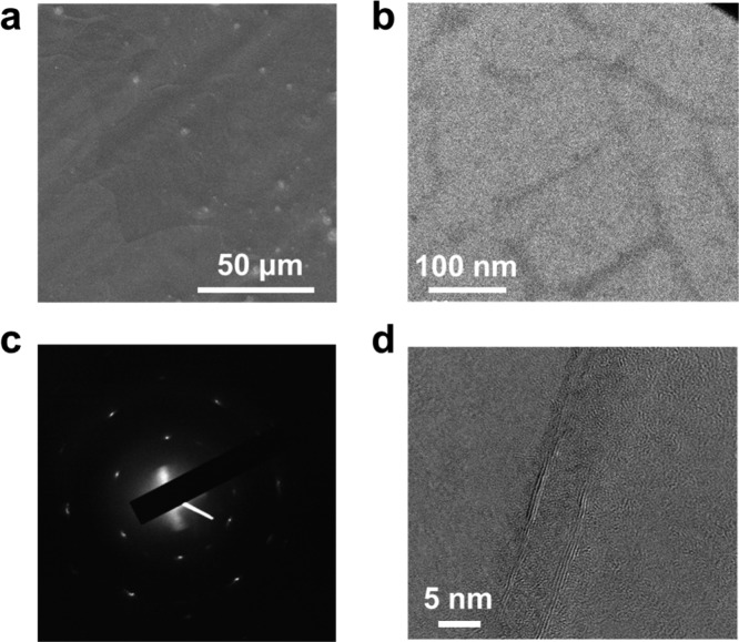
To examine the formation of BNNT networks within the graphene layer, scanning electron microscope (SEM) images of RGBNNT transferred to a SiO2/Si substrate are shown in Figure 2a and Supporting Information Figure S7; almost no obvious BNNT bundles are observed, indicating the formation of a 2D hybrid sheet similar to rebar graphene with CNTs.17 The as-produced RGBNNT was transferred onto a transmission electron microscope (TEM) grid for further characterization. From a representative TEM image (Figure 2b), a BNNT network could be observed on the continuous 2D sheets. The existence of the underlying graphene sheet was examined by selected area electron diffraction (SAED) (Figure 2c), and the hexagonal crystalline structure of graphene could be confirmed.21 From a higher resolved TEM image (Figure 2d and Supporting Information Figure S8), the partial unzipping of a BNNT is observed with the disappearance of part of the sidewall of the BNNT, suggesting the covalent interaction between BNNT sidewalls and the graphene sheet, as it is widely reported that BN atoms can covalently network with CNTs11,12 or graphene14,15 based on the shared hexagonal structure to generate the BCN structure. Further evidence of BCN hybridization is provided by electron energy loss spectroscopy (EELS) elemental mapping shown in Supporting Information Figure S9. It is observed that B and N atoms are mostly distributed along the BNNT, with some diffusion into the graphene layer, as a result of the BCN hybridization. The C atoms, on the other hand, are uniformly distributed within the image area. The covalent BCN hybridzation should in turn cause the increase of D band in the Raman spectra of RGBNNT as the atomic structure of graphene is influenced by BN introduction.13,15
Figure 2.
(a) Typical SEM image of transferred RGBNNT (method 1) on a SiO2/Si substrate; very few obvious BNNT bundles were observed. (b) Typical TEM image of BNNT networks within a RGBNNT (method 3) layer. (c) SAED pattern of a RGBNNT film (method 3) on a TEM grid; the hexagonal pattern corresponds to the hexagonal structure of the graphene sheet. (d) A TEM image of partially unzipped BNNTs within the RGBNNT film (method 3).
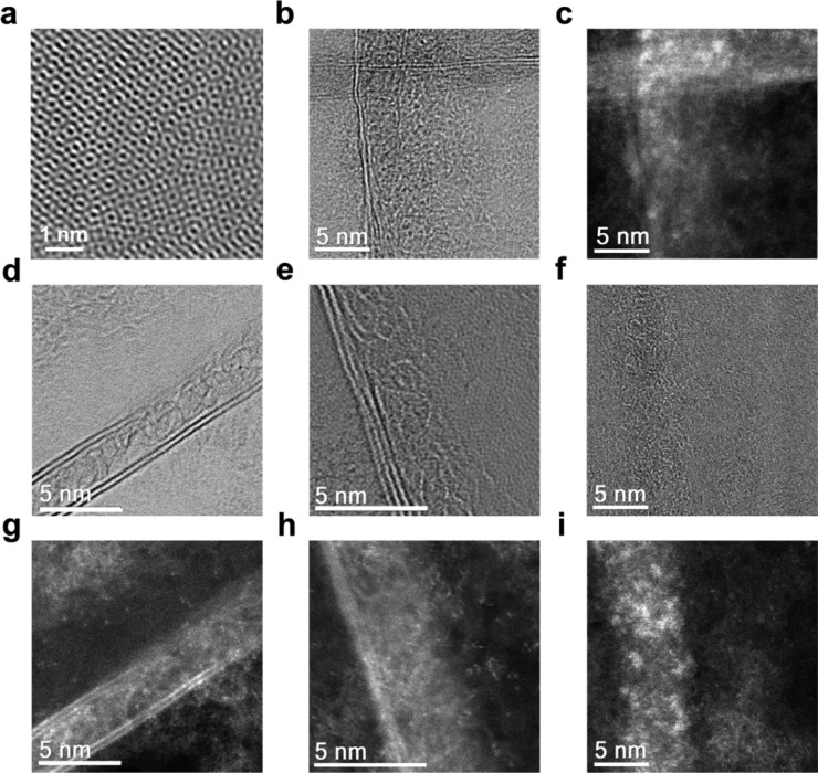
To further characterize the behavior of BNNTs within the monolayer graphene sheet, atomic resolution scanning transmission electron microscopy (AR-STEM, Figure 3) images of RGBNNT (method 3) were taken. To confirm the hexagonal structure of graphene, an AR-STEM image was first taken on a graphene sheet without any appearance of BNNTs. From Supporting Information Figure S10 (without filter) and Figure 3a (with filter), the hexagonal atomic structure of the graphene sheet is observed, and the distorted direction of the hexagons indicates the graphene sheet is polycrystalline with the existence of grain boundaries.36Figure 3b,d–f are the bright field (BF) AR-STEM images, and Figure 3c,g–i are the dark field (DF) AR-STEM images of BNNTs within the graphene layer. Figure 3b,c shows two interconnected BNNTs with an intersection angle of ∼90°; these two BNNTs are part of the BNNT network that strengthens the underlying 2D layer. Figures 3d and 3g show a BNNT with a section of the sidewall gone that unzipped and merged with the graphene forming BCN hybrid. Figure 3e,h shows a BNNT where the left side of the sidewall remains intact while the right side of the wall is completely decomposed. Figure 3f,I shows a BNNT with both sidewalls gone, which could be defined as a BN nanoribbon instead of a BNNT. Interestingly, from these images, the BNNTs have partially unzipped and the atoms have merged into the graphene layer, resulting in a BCN hybrid structure.
Figure 3.
AR-STEM images of a RGBNNT film (method 3). (a) A BF AR-STEM image of RGBNNT with filter applied. (b, d–f) BF AR-STEM and (c, g–i) DF AR-STEM images of BNNTs within the RGBNNT film. (b and c) Two interconnected BNNTs; (d and g) a BNNT with a section of the sidewall gone (unzipped); (e and h) a partially unzipped BNNT with the walls at one side merged into the graphene film; (f and i) a completely unzipped BNNT with walls on both sides merged into the graphene film.
Because two types of interaction, noncovalent interaction and covalent bonding, could exist between the graphene and BNNTs, a control experiment was designed to demonstrate that the enhanced mechanical strength of RGBNNT results primarily from the covalent bonding between graphene and BNNT domains. A graphene film grown on Cu was spin-coated with BNNTs, and then etched without PMMA protection in the same way as the RGBNNT sample. This control sample, with only noncovalent interaction between the spin-coated BNNTs and graphene, broke into pieces in 1% butanol in H2O. Hence, the covalent reinforcement is required for increased mechanical strength.
To analyze the elemental composition of the RGBNNT, X-ray photoelectron spectroscopy (XPS) spectra were taken of the as-grown RGBNNT on the Cu foils (Figure 4 and Supporting Information Figures S11–S14). Since the RGBNNT is mainly composed of graphene, the position of 284.5 eV for sp2 C 1s peak is used as standard to shift all other peaks.17,37 After calibration, the B 1s peak is located at 189.8 eV, and the N 1s peak is located at 397.5 eV; both energies are similar to the values reported for h-BN38 or other BCN hybrid structures.13,15 Interestingly, a side peak of N 1s is observed at 400.2 eV, corresponding to the N–C bond as is reported with N-doped graphene,39 which provides further evidence toward the covalent interaction between partially unzipped BNNT and graphene sheet; no obvious side peak of B 1s is observed due to the low S/N ratio. The concentrations of B and N atoms within RGBNNT were found to be 2 to 3%, indicating carbon is the dominant part of the 2D hybrid film.
Figure 4.

XPS spectra of RGBNNT (method 1). (a) Survey, (b) B 1s, (c) C 1s, (d) N 1s.
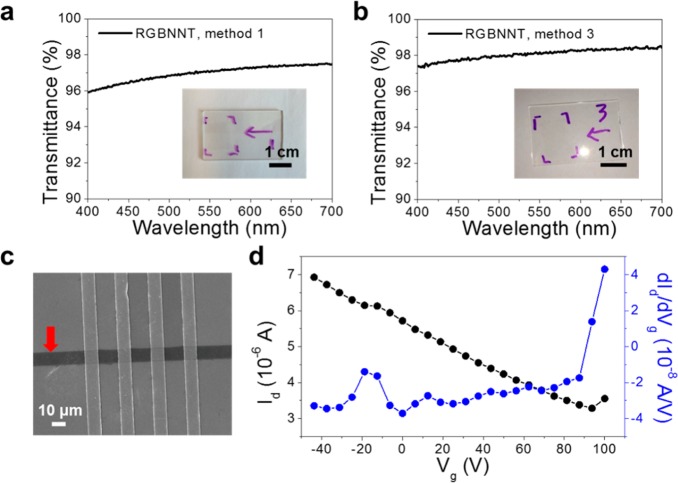
To further characterize the properties of RGBNNT, the as-grown RGBNNT films were transferred onto glass slides, using the polymer-free method, for transmittance and conductivity measurements (Figure 5a,b). For RGBNNT made from method 1, the transmittance at 550 nm was 97.0% with a sheet resistance of 36 kΩ/□. For RGBNNT made from method 3, the transmittance at 550 nm was 98.1% with a sheet resistance of 24 kΩ/□. The resistance of RGBNNT is significantly higher than that of monolayer graphene (∼1 kΩ/□)33 or rebar graphene with CNTs (0.6 kΩ/□);17 this is a result of the impregnation of graphene by insulating BNNTs. A noncovalent interaction should not significantly lower the electrical conductivity of an intact graphene layer, further suggesting the hybridization through covalent interaction in the RGBNNT. As for optical transmittance, RGBNNT has the same transmittance value as monolayer graphene (97.4%)33 at 550 nm; BNNTs absorb little light in the visible region,7 while the high optical absorbance of CNTs makes rebar graphene with CNTs (95.6%)17 slightly darker.
Figure 5.
UV–vis spectra of RGBNNT films transferred onto glass slides without the assistance of a polymer. (a) RGBNNT made from method 1, the transmittance at 550 nm was 97.0% with a sheet resistance of 36 kΩ/□ (insert is a photograph of the film on glass). (b) RGBNNT made from method 3, the transmittance at 550 nm was 98.1% with a sheet resistance of 24 kΩ/□ (inset is a photograph of the film on glass). (c) A SEM image of the fabricated RGBNNT (method 1) FET on 300 nm SiO2/highly doped p-type Si substrate; the red arrow is pointed at the RGBNNT nanoribbon with a width of 10 μm. The four Au electrodes with a separation distance of 14 μm are 90° to the RGBNNT. (d) The drain current as a function of the voltage applied to the back (bottom) gate of the device shown in (c). And the derivative of the drain current vs the back gate voltage. The source-drain voltage was 1 V.
To investigate the electrical properties of RGBNNT, a FET was fabricated on a lithography-cut strip of the RGBNNT (method 1). The strip was on SiO2 (300 nm)/highly doped p-type Si with four electrodes and tested at 10–5–10–6 Torr at room temperature, as shown in Figure 5c. Figure 5d shows the Vg–Id curve with the back-gate voltage ranging from −40 to 100 V at Vd = 1 V. The RGBNNTs shows an ambipolar semiconducting behavior (typical of CVD graphene3,33,40) with a charge-neutrality point at ∼95 V, which indicates highly p-doped material due to the BNNT hybridization on the graphene grain boundaries, in agreement with other BCN hybrid structures.13,15,41 The carrier mobility of the RGBNNT FET device was ∼20 cm2V–1s–1 based on the slope of Id variation with back-gate voltages. This is much smaller than the mobility reported for rebar graphene with CNTs (1500–2200 cm2V–1s–1)17 or single layer graphene (2000–4000 cm2 V–1 s–1)3,33,40 on SiO2. This can be attributed to the scattering of electrons at the interfaces or boundaries between the graphene and BNNT domains, similar to that seen in CVD hexagonal BCN FET devices (5–20 cm2V–1s–1).13 These results are consistent with the RGBNNT components being covalently bonded rather than having solely a BNNT/graphene stacking structure. The ON/OFF ratio of this FET device was ∼2.5, similar to that seen in single-layer graphene (1–5),3,33,40 and also similar to CVD h-BCN devices (1–2).13
Conclusions
RGBNNT was successfully synthesized using functionalized BNNTs. Similar to rebar graphene with CNTs, BNNTs formed a rebar network within the graphene layer, and enhanced the mechanical strength of graphene, making it possible to transfer the layer to another substrate without assistance from a polymer. The BNNT-graphene interface was investigated using AR-STEM, and it was shown that BNNTs were partially unzipped and merged into the graphene layer to generate a BCN hybrid structure, which resulted in an increased D band in the Raman spectra and an increased sheet resistance. The electronic properties of the RGBNNT were measured using a FET. The synthesis of this new kind of 2D hybrid provides an alternative and easy approach toward the hybridization between C and BN nanostructures, while the extension into other graphene-like 2D hybrid structures is foreseeable.
Methods
The Raman spectra were recorded with a Renishaw Raman RE01 scope. SEM images were taken using a JEOL 6500F Scanning Electron Microscope. TEM characterizations were performed using a 200 kV JEOL FE2100 TEM. STEM images were collected with a JEOL JEM-ARM200F operated at 80 kV equipped with a Cs probe corrector. A six-probe station (Desert Cryogenic TT-probe 6 system) was used to measure the electrical properties under a pressure of 10–5–10–6 Torr at room temperature using an Agilent B1500A Semiconductor Device Analyzer. XPS was performed on a PHI Quantera SXM scanning X-ray microprobe with 100 μm beam size and 45° takeoff angle, and calibrated using C 1s at 284.5 eV.
Acknowledgments
This work was funded by the Air Force Office of Scientific Research (AFOSR) (FA9550-14-1-0111), the AFOSR MURI (FA9550-12-1-0035), the Office of Naval Research MURI program (#00006766, N00014-09-1-1066), the National Center for Research Resources (5 G12RR013646-12), NSF-PREM (DMR 0934218) and the National Institute on Minority Health and Health Disparities (G12MD007591) from the National Institutes of Health. We thank Cheol Park and Catharine Fay for establishing a material transfer agreement between NASA Langley Research Center and Rice University, which enabled Rice University to obtain the BNNTs.
Supporting Information Available
Includes materials and methods and additional graphs. This material is available free of charge via the Internet at http://pubs.acs.org.
Author Contributions
# These authors (Y.L. and Z.P.) contributed equally to the work.
The authors declare no competing financial interest.
Funding Statement
National Institutes of Health, United States
Supplementary Material
References
- Geim A. K.; Novoselov K. S. The Rise of Graphene. Nat. Mater. 2007, 6, 183–191. [DOI] [PubMed] [Google Scholar]
- Geim A. K. Graphene: Status and Prospects. Science 2009, 324, 1530–1534. [DOI] [PubMed] [Google Scholar]
- Kim K. S.; Zhao Y.; Jang H.; Lee S. Y.; Kim J. M.; Kim K. S.; Ahn J.-H.; Kim P.; Choi J.-Y.; Hong B. H. Large-Scale Pattern Growth of Graphene Films for Stretchable Transparent Electrodes. Nature 2009, 457, 706–710. [DOI] [PubMed] [Google Scholar]
- Li X.; Zhu Y.; Cai W.; Borysiak M.; Han B.; Chen D.; Piner R. D.; Colombo L.; Ruoff R. S. Transfer of Large-Area Graphene Films for High-Performance Transparent Conductive Electrodes. Nano Lett. 2009, 9, 4359–4363. [DOI] [PubMed] [Google Scholar]
- Lin Y.-M.; Dimitrakopoulos C.; Jenkins K. A.; Farmer D. B.; Chiu H.-Y.; Grill A.; Avouris P. 100-GHz Transistors from Wafer-Scale Epitaxial Graphene. Science 2010, 327, 662–662. [DOI] [PubMed] [Google Scholar]
- Dean C.; Young A.; Meric I.; Lee C.; Wang L.; Sorgenfrei S.; Watanabe K.; Taniguchi T.; Kim P.; Shepard K. Boron Nitride Substrates for High-Quality Graphene Electronics. Nat. Nanotechnol. 2010, 5, 722–726. [DOI] [PubMed] [Google Scholar]
- Golberg D.; Bando Y.; Tang C.; Zhi C. Boron Nitride Nanotubes. Adv. Mater. 2007, 19, 2413–2432. [Google Scholar]
- Golberg D.; Bando Y.; Huang Y.; Terao T.; Mitome M.; Tang C.; Zhi C. Boron Nitride Nanotubes and Nanosheets. ACS Nano 2010, 4, 2979–2993. [DOI] [PubMed] [Google Scholar]
- Watanabe K.; Taniguchi T.; Kanda H. Direct-Bandgap Properties and Evidence for Ultraviolet Lasing of Hexagonal Boron Nitride Single Crystal. Nat. Mater. 2004, 3, 404–409. [DOI] [PubMed] [Google Scholar]
- Kawaguchi M.; Kawashima T.; Nakajima T. Syntheses and Structures of New Graphite-like Materials of Composition BCN(H) and BC3N(H). Chem. Mater. 1996, 8, 1197–1201. [Google Scholar]
- Stephan O.; Ajayan P.; Colliex C.; Redlich P.; Lambert J.; Bernier P.; Lefin P. Doping Graphitic and Carbon Nanotube Structures with Boron and Nitrogen. Science 1994, 266, 1683–1685. [DOI] [PubMed] [Google Scholar]
- Golberg D.; Bando Y.; Han W.; Kurashima K.; Sato T. Single-Walled B-Doped Carbon, B/N-Doped Carbon and BN Nanotubes Synthesized from Single-Walled Carbon Nanotubes through a Substitution Reaction. Chem. Phys. Lett. 1999, 308, 337–342. [Google Scholar]
- Ci L.; Song L.; Jin C.; Jariwala D.; Wu D.; Li Y.; Srivastava A.; Wang Z.; Storr K.; Balicas L. Atomic Layers of Hybridized Boron Nitride and Graphene Domains. Nat. Mater. 2010, 9, 430–435. [DOI] [PubMed] [Google Scholar]
- Wang S.; Zhang L.; Xia Z.; Roy A.; Chang D. W.; Baek J. B.; Dai L. BCN Graphene as Efficient Metal-Free Electrocatalyst for the Oxygen Reduction Reaction. Angew. Chem., Int. Ed. 2012, 51, 4209–4212. [DOI] [PubMed] [Google Scholar]
- Gong Y.; Shi G.; Zhang Z.; Zhou W.; Jung J.; Gao W.; Ma L.; Yang Y.; Yang S.; You G. Direct Chemical Conversion of Graphene to Boron- and Nitrogen- and Carbon-Containing Atomic Layers. Nat. Commun. 2014, 5, 3193. [DOI] [PubMed] [Google Scholar]
- Shinde P. P.; Kumar V. Direct Band Gap Opening in Graphene by BN Doping: Ab initio Calculations. Phys. Rev. B 2011, 84, 125401. [Google Scholar]
- Yan Z.; Peng Z.; Casillas G.; Lin J.; Xiang C.; Zhou H.; Yang Y.; Ruan G.; Raji A.-R. O.; Samuel E. L. G.; et al. Rebar Graphene. ACS Nano 2014, 8, 5061–5068. [DOI] [PMC free article] [PubMed] [Google Scholar]
- Smith M. W.; Jordan K. C.; Park C.; Kim J.-W.; Lillehei P. T.; Crooks R.; Harrison J. S. Very Long Single- and Few-Walled Boron Nitride Nanotubes via the Pressurized Vapor/Condenser Method. Nanotechnology 2009, 20, 505604. [DOI] [PubMed] [Google Scholar]
- Ciofani G.; Genchi G. G.; Liakos I.; Athanassiou A.; Dinucci D.; Chiellini F.; Mattoli V. A Simple Approach to Covalent Functionalization of Boron Nitride Nanotubes. J. Colloid Interface Sci. 2012, 374, 308–314. [DOI] [PubMed] [Google Scholar]
- Zhi C.; Bando Y.; Tang C.; Honda S.; Sato K.; Kuwahara H.; Golberg D. Covalent Functionalization: Towards Soluble Multiwalled Boron Nitride Nanotubes. Angew. Chem., Int. Ed. 2005, 44, 7932–7935. [DOI] [PubMed] [Google Scholar]
- Emtsev K. V.; Bostwick A.; Horn K.; Jobst J.; Kellogg G. L.; Ley L.; McChesney J. L.; Ohta T.; Reshanov S. A.; Röhrl J. Towards Wafer-Size Graphene Layers by Atmospheric Pressure Graphitization of Silicon Carbide. Nat. Mater. 2009, 8, 203–207. [DOI] [PubMed] [Google Scholar]
- Ferrari A.; Meyer J.; Scardaci V.; Casiraghi C.; Lazzeri M.; Mauri F.; Piscanec S.; Jiang D.; Novoselov K.; Roth S. Raman Spectrum of Graphene and Graphene Layers. Phys. Rev. Lett. 2006, 97, 187401. [DOI] [PubMed] [Google Scholar]
- Sun Z.; Raji A.-R. O.; Zhu Y.; Xiang C.; Yan Z.; Kittrell C.; Samuel E. L. G.; Tour J. M. Large-Area Bernal-Stacked Bi-, Tri-, and Tetralayer Graphene. ACS Nano 2012, 6, 9790–9796. [DOI] [PubMed] [Google Scholar]
- Edwards R. S.; Coleman K. S. Graphene Film Growth on Polycrystalline Metals. Acc. Chem. Res. 2012, 46, 23–30. [DOI] [PubMed] [Google Scholar]
- Ruan G.; Sun Z.; Peng Z.; Tour J. M. Growth of Graphene from Food, Insects, and Waste. ACS Nano 2011, 5, 7601–7607. [DOI] [PubMed] [Google Scholar]
- Sun Z.; Yan Z.; Yao J.; Beitler E.; Zhu Y.; Tour J. M. Growth of Graphene from Solid Carbon Sources. Nature 2010, 468, 549–552. [DOI] [PubMed] [Google Scholar]
- Yan Z.; Peng Z.; Sun Z.; Yao J.; Zhu Y.; Liu Z.; Ajayan P. M.; Tour J. M. Growth of Bilayer Graphene on Insulating Substrates. ACS Nano 2011, 5, 8187–8192. [DOI] [PubMed] [Google Scholar]
- Peng Z.; Yan Z.; Sun Z.; Tour J. M. Direct Growth of Bilayer Graphene on SiO2 Substrates by Carbon Diffusion through Nickel. ACS Nano 2011, 5, 8241–8247. [DOI] [PubMed] [Google Scholar]
- Pimenta M.; Dresselhaus G.; Dresselhaus M. S.; Cancado L.; Jorio A.; Saito R. Studying Disorder in Graphite-Based Systems by Raman Spectroscopy. Phys. Chem. Chem. Phys. 2007, 9, 1276–1290. [DOI] [PubMed] [Google Scholar]
- Geick R.; Perry C.; Rupprecht G. Normal Modes in Hexagonal Boron Nitride. Phys. Rev. 1966, 146, 543. [Google Scholar]
- Arenal R.; Ferrari A.; Reich S.; Wirtz L.; Mevellec J.-Y.; Lefrant S.; Rubio A.; Loiseau A. Raman Spectroscopy of Single-Wall Boron Nitride Nanotubes. Nano Lett. 2006, 6, 1812–1816. [DOI] [PubMed] [Google Scholar]
- Reina A.; Jia X.; Ho J.; Nezich D.; Son H.; Bulovic V.; Dresselhaus M. S.; Kong J. Large Area, Few-Layer Graphene Films on Arbitrary Substrates by Chemical Vapor Deposition. Nano Lett. 2009, 9, 30–35. [DOI] [PubMed] [Google Scholar]
- Suk J. W.; Kitt A.; Magnuson C. W.; Hao Y.; Ahmed S.; An J.; Swan A. K.; Goldberg B. B.; Ruoff R. S. Transfer of CVD-Grown Monolayer Graphene onto Arbitrary Substrates. ACS Nano 2011, 5, 6916–6924. [DOI] [PubMed] [Google Scholar]
- Song L.; Ci L.; Lu H.; Sorokin P. B.; Jin C.; Ni J.; Kvashnin A. G.; Kvashnin D. G.; Lou J.; Yakobson B. I. Large Scale Growth and Characterization of Atomic Hexagonal Boron Nitride Layers. Nano Lett. 2010, 10, 3209–3215. [DOI] [PubMed] [Google Scholar]
- van der Zande A. M.; Huang P. Y.; Chenet D. A.; Berkelbach T. C.; You Y.; Lee G.-H.; Heinz T. F.; Reichman D. R.; Muller D. A.; Hone J. C. Grains and Grain Boundaries in Highly Crystalline Monolayer Molybdenum Disulphide. Nat. Mater. 2013, 12, 554–561. [DOI] [PubMed] [Google Scholar]
- Kim K.; Lee Z.; Regan W.; Kisielowski C.; Crommie M.; Zettl A. Grain Boundary Mapping in Polycrystalline Graphene. ACS Nano 2011, 5, 2142–2146. [DOI] [PubMed] [Google Scholar]
- Bae S.; Kim H.; Lee Y.; Xu X.; Park J.-S.; Zheng Y.; Balakrishnan J.; Lei T.; Kim H. R.; Song Y. I. Roll-to-Roll Production of 30-in. Graphene Films for Transparent Electrodes. Nat. Nanotechnol. 2010, 5, 574–578. [DOI] [PubMed] [Google Scholar]
- Miyamoto Y.; Rubio A.; Cohen M. L.; Louie S. G. Chiral Tubules of Hexagonal BC2N. Phys. Rev. B 1994, 50, 4976. [DOI] [PubMed] [Google Scholar]
- Lv R.; Li Q.; Botello-Méndez A. R.; Hayashi T.; Wang B.; Berkdemir A.; Hao Q.; Elías A. L.; Cruz-Silva R.; Gutiérrez H. R.; et al. Nitrogen-doped graphene: beyond single substitution and enhanced molecular sensing. Sci. Rep. 2012, 2. [DOI] [PMC free article] [PubMed] [Google Scholar]
- Li X.; Cai W.; An J.; Kim S.; Nah J.; Yang D.; Piner R.; Velamakanni A.; Jung I.; Tutuc E.; et al. Large-Area Synthesis of High-Quality and Uniform Graphene Films on Copper Foils. Science 2009, 324, 1312–1314. [DOI] [PubMed] [Google Scholar]
- Watanabe M.; Itoh S.; Mizushima K.; Sasaki T. Electrical Properties of BC2N Thin Films Prepared by Chemical Vapor Deposition. J. Appl. Phys. 1995, 78, 2880–2882. [Google Scholar]
Associated Data
This section collects any data citations, data availability statements, or supplementary materials included in this article.


