Abstract
Amorphous Ge2Sb2Te5 (GST) alloy, upon heating crystallize to a metastable NaCl structure around 150°C and then to a stable hexagonal structure at high temperatures (≥250°C). It has been generally understood that the phase change takes place between amorphous and the metastable NaCl structure and not between the amorphous and the stable hexagonal phase. In the present work, it is observed that the thermally evaporated (GST)1-xSex thin films (0 ≤ x ≤ 0.50) crystallize directly to the stable hexagonal structure for x ≥ 0.10, when annealed at temperatures ≥ 150°C. The intermediate NaCl structure has been observed only for x < 0.10. Chemically ordered network of GST is largely modified for x ≥ 0.10. Resistance, thermal stability and threshold voltage of the films are found to increase with the increase of Se. The contrast in electrical resistivity between the amorphous and crystalline phases is about 6 orders of magnitude. The increase in Se shifts the absorption edge to lower wavelength and the band gap widens from 0.63 to 1.05 eV. Higher resistance ratio, higher crystallization temperature, direct transition to the stable phase indicate that (GST)1-xSex films are better candidates for phase change memory applications.
It is well known that Ge2Sb2Te5 (GST) alloy undergo reversible phase transition between the amorphous and crystalline states by laser irradiation or electrical pulses1,2. Upon applying an electric field, low conductive amorphous state crosses a threshold voltage (Vth) and permanently changes to a high conductive crystalline state due to the Joule heating (SET transition). To revert back to the amorphous state, a nano second pulse with very low rise and fall time is applied. This increases the temperature of the crystalline GST above its melting point (Tm) and then the material rapidly cooled back to room temperature which happens within 10–30 ns (RESET transition). The amorphous and crystalline phases have large resistance contrast, at least a minimum of 103. This property of GST alloys is exploited for the phase change random access memory (PCRAM) applications.
The rate of crystallization, thermal stability and the contrast in electrical resistivity and optical reflectivity are very important for an efficient phase change material. In Ge–Sb–Te along the Sb2Te3–GeTe pseudo binary tie-line the thermal stability increases but the crystallization speed decrease. At the extreme ends of this tie-line, GeTe has higher thermal stability and less crystallization speed while Sb2Te3 has higher crystallization speed and lower thermal stability. Ge2Sb2Te5 is an intermediate compound in the tie-line and so has a best combination of thermal stability and crystallization speed. However, the low thermal stability and the requirement of higher RESET current due to higher Tm (616°C) are some of the concerns3,4.
Another aspect is the toxicity of Te due to which Te is less preferred for semiconductor manufacturing processes. Selenium is less toxic than Te, hence a constant effort is being made to use more of Se in place of Te in the phase change memory (PCM) alloys3. An increase in electrical resistivity and a decrease in crystallization temperature (Tc) has been observed in GeSb2Te4 when Se is substituted for Te3. GeSb2Te3Se shows usual amorphous to NaCl and then to hexagonal transition even after 25 at.% of Te sites are substituted by Se. In the rock salt structure of GST, 20% of vacancy is reported in Ge/Sb sublattice, whereas hexagonal structure has none4. Other Se alloys such as Ga–Sb–Se, Sb–Se possess higher Tc, better data retention, higher switching speed, lower thermal conductivity and lower Tm with respect to GST, but the resistance ratio is limited to about two orders of magnitude5,6. If a comparable resistance ratio along with a higher Tc can be obtained by doping GST with a suitable material, it would be beneficial. In this work, an attempt has been made to improve the phase change properties of GST by the addition of Se for PCM applications.
Results and Discussion
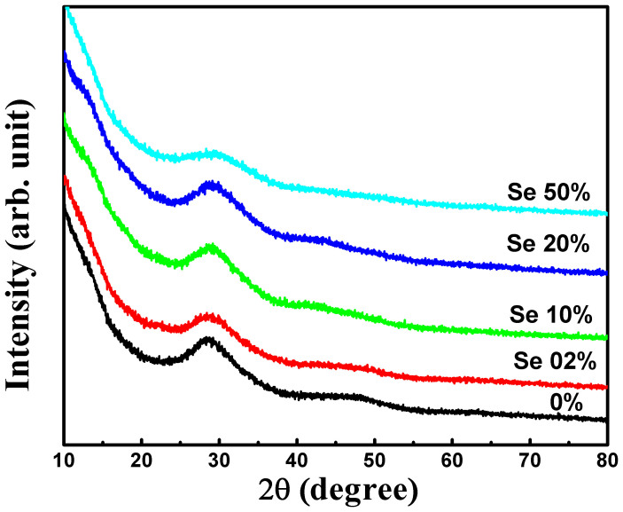
The XRD spectra shown in Fig. 1 indicate the amorphous nature of the as deposited (AD) (GST)1-xSex films. The films annealed at 150°C and 300°C are shown in Fig. 2. The crystalline structure of GST and (GST)0.98Se0.02 films annealed at 150°C are identified as NaCl with space group Fm-3m (Fig. 2a) (04-011-9024 ICDD 2012)7. Interestingly the films with x = 0.10 and 0.20 crystallized into hexagonal structure which was not expected (04-006-9784 ICDD 2012)8. The peak intensity of these alloys decreases with the increase of Se indicating increased amorphousness in the alloys. The presence of Se may suppress the crystallization of GST and therefore a very small percentage of GST nucleates with small crystallite size. The decrease in peak intensity and broadening of the peaks indicate a decrease in grain size for Se doped GST films. Similar kind of decrease in grain size has been observed in Ag doped GST9. The (GST)0.50Se0.50 film remain amorphous and does not crystallize. The films annealed at 300°C crystallized into hexagonal structure as shown in Fig. 2(b).
Figure 1. XRD pattern of (GST)1-Sex films in the as deposited state.
Figure 2. XRD patterns of (GST)1-xSex films annealed at (a)150°C and (b) 300°C.
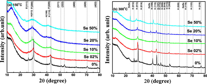
It is interesting to note that the intermediate NaCl phase disappeared with the Se doping. Atomic distribution of GST in crystalline NaCl structure closely resembles that of its amorphous phase10. This necessitates only a small change in local structure during the phase transformation. Kolobov et al. suggest that the coordination of Ge atoms changes from octahedral to tetrahedral co-ordination (Umbrella flip) during the phase change11. There is Ge–Te, Sb–Te bonds in the first neighbor interactions and Te–Te bonds in the second neighbor interactions in both amorphous and crystalline phases11. Amorphous phase has bonded with natural valency followed by 8-N rule and NaCl structure has 6 fold co-ordinations. In NaCl structure of GST, the 4a site is wholly occupied by Te and the 4b site is randomly occupied by Ge or Sb or 20% vacancies10. The transition from NaCl to hexagonal happens with minimum changes and with the conservation of bond lengths12.
Zhimei Sun et al.12 discussed that the metastable GST does not possess a cubic structure, rather consists of two well-defined highly ordered three-dimensional repeat units: –Te–Ge–Te–Sb–Te– (I) and –Te–Sb–Te–Ge– (II). These two units repeat and are bonded alternatively in space consistent with a NaCl structure. The phase transition from NaCl to hexagonal is made possible by the movement of unit II in the [210] direction. And there exist a weak bonding between Te layer of each unit to others and phase change is possible by the movement of Te planes12.
Upon heating, GST films crystallize to NaCl structure and then to hexagonal structure at 150°C and 250°C respectively13. Ag doped GST show direct amorphous to NaCl transition and no indication of hexagonal phase transition in the studied temperature range (up to 300°C)9. This study ruled out the possibility of Ag occupancy in the vacancies but suggest the possibility of Ag atoms being occupied at the grain boundaries. Atomic radius of Ag is 165 pm and atomic weight is 107.9 amu, which can be compared with the atoms present in the GST alloy (Table 1). It was found that in Ge2Sb2+xTe5 alloys, Sb atoms added beyond the stoichiometric ratio do not enter the lattice site of the NaCl type crystal to fill up the vacancies but remain at the grain boundaries and suppresses the crystal growth10. Phase separation has been observed in the non-stoichiometric alloys rich with Ge14. Indium doped GST (In0.3Ge2Sb2Te5) show a mixed phase of dominant cubic structure and a small amount of In2Te3 when annealed at 180°C15. Amorphous to cubic transition was observed above 220°C in Si doped GST for Si ≥ 11.8 at. % whereas the Si < 11.8 at.% shows amorphous to NaCl and then to hexagonal transitions above 170°C. The smaller atomic size and atomic weight and higher electronegativity of Se influence the structural transitions in GST.
Table 1. Atomic weight, atomic radius and electronegativity of Ge, Sb, Te and Se elements.
| Ge | Sb | Te | Se | |
|---|---|---|---|---|
| At wt.(amu) | 72.64 | 121.76 | 127.60 | 78.96 |
| At radius (pm) | 125 | 133 | 123 | 103 |
| Electronegativity (Pauling scale) | 2.01 | 2.05 | 2.1 | 2.55 |
In chalcogenides, the variations of physical properties with composition are well understood with the constraint counting model proposed by Phillips and Thorpe16. According to this model the network transform from floppy (under-coordinated network) to a rigid structure (over-coordinated network) at an average coordination Zav = 2.4. The critical composition at which this transition occurs is called the rigidity percolation threshold (RPT). There is another transition called chemical threshold (CT) which usually occurs at higher coordination numbers. In IV–VI glasses CT occurs at Zav = 2.67 and for V–VI glasses both the RPT and CT coincides at Zav = 2.4. At CT, the network has a maximum ordering and is closest to the crystalline state17. The molar volume is also exhibits a maximum at CT. Interestingly; the average co-ordination number of GST is 2.67, which corresponds to the chemically ordered network structure. This chemical ordering could be one of the reasons for the ease of transition between amorphous and crystalline states in GST alloy. Addition of Se to GST, decreases the average coordination number (see Table 2). The decrease in average coordination number indicates the decrease in the network rigidity, molar volume and deviation from chemical ordering. Hence, with the increase of Se, crystallization may become difficult. There should be a critical composition at which this decrease in average coordination, molar volume, rigidity and chemical ordering should largely affect the crystallization and thereby the phase change properties. In the (GST)1-xSex alloys this critical coordination occurs at x ≥ 0.10 (Zav = 2.6) where the intermediate NaCl phase disappears and the alloy directly undergo amorphous to hexagonal transition.
Table 2. Average co-ordination number of the alloys.
| (Ge2Sb2Te5)1-xSex | x = 0.0 | x = 0.02 | x = 0.10 | x = 0.20 | x = 0.50 |
|---|---|---|---|---|---|
| Co-ord. no. | 2.67 | 2.65 | 2.6 | 2.53 | 2.33 |
Out of the three well known phases of GST, the stable hexagonal phase consists of cycling nine layers of –Te–Ge/Sb–Te–Ge/Sb–Te–Te–Ge/Sb–Te–Ge/Sb– in the ABCABCABC packing in one unit cell (space group P-3m1 with lattice parameter a = 4.2 Å, c = 16.96 Å)18. Metastable NaCl structure can also be considered as six layered structure, –Te–Ge/Sb–Te–Ge/Sb–Te–Ge/Sb–, in the hexagonal notation in which alternate stacks of Te and Ge/Sb layer are cycled along c-axis4. This leads to a conclusion that the stable hexagonal phase can be considered as NaCl layers stacked along the c-axis forming nine layers, except the Te–Te layer. Considering metastable structure having vacancy (20 at.%) and stable phase having a Te–Te layer (without vacancy), it would be possible that Se occupies the rock salt structure vacancies and forms an Te–Te or Se–Te van der Waals bonded layers, and can possibly leads to a hexagonal structure. The above models are based on the fact that both metastable and stable phases are fundamentally similar to each other, when Te and Ge/Sb stacked alternatively. However, these assumptions need a detailed study. The general understanding is that the metastable NaCl-like structure is important for crystallization process in phase change GST alloys19. The amorphous to hexagonal transition in the Se doped GST alloys also results in the reversible switching with comparable threshold voltages.
Raman spectroscopy can be used to probe medium range order in glasses and crystalline materials. It is a very sensitive tool for studying PCM materials since photons can directly couple with lattice vibrations and inherently reflect the local symmetry. It is important to use appropriate measurement time and low power density laser beam in order to avoid laser induced crystallization of GST film. The accumulation time of the measurement is fixed to 180 seconds for varying power densities. Power of the laser can be reduced by using various filters. Spectra of GST AD films for varying power densities are shown in Fig. 3.
Figure 3. The spectra of GST for various filter-power combinations.
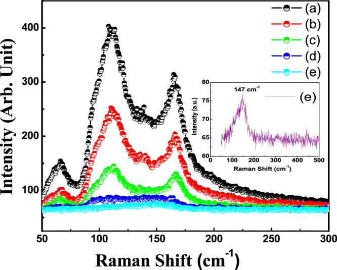
(a) 3 mW laser power without filter, (b) 1 mW without filter, (c) 1 mW with D0.3, (d) 1 mW with D1, (e) 1 mW with D2. Inset shows the enlarge spectra of 3(e) resulting from the amorphous GST.
Raman bands centered at 110 and 165 cm−1 seen in Fig. 3(a–d) are characteristic of crystalline GST, signifying the laser induced crystallization in the sample. Cho et al. and Liu et al.20,21 observed Raman peaks for c-GST at 110 cm−1 corresponding to the vibration of hetero polar bond in the tetrahedral GeTe4 and/or pyramidal SbTe3. The band at 160 cm−1 is due to Sb–Sb vibrations in (Te2)Sb–Sb(Te2) or (TeSb)Sb–Sb(Te2)11,20,21,22,23,24 In Fig. 3(e) and the inset, a band centered at 147 cm−1 has been observed which originates from the amorphous GST. This band is believed to originate from SbTe3 pyramids or edge sharing GeTe4 tetrahedral vibrational modes11,19,20. As the power of the laser decreases or filtering increases, the surface crystallization disappears.
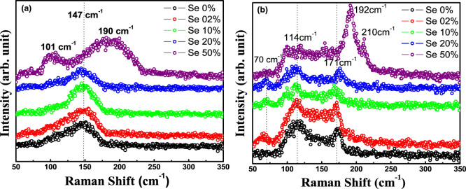
Fig. 4 show Raman spectra of AD and annealed (GST)1-xSex films. Amorphous GST has a Raman band centered at 147 cm−1. The Raman spectrum of a-GST and a-Sb2Te3 is very similar25. For films annealed at 300°C, peaks are observed at around 114 and 171 cm−1 (Fig. 4(b)). The peak observed at 171 cm−1 is due to the hexagonal structure. A peak at 160 cm−1 for the NaCl structure gets shifted to higher wave numbers in the hexagonal structure as reported by Bastiani et al.26 When atomic weight of the doped elements is less, the peak position shifts to higher wave number27. The peak shift and broadening indicate the change in the bond length and bond angles27. The band at 190–192 cm−1 is observed in both AD and annealed thin films of (GST)0.50Se0.50. For GeSe4 tetrahedra vibrations, Raman bands are observed at 200 and 215 cm−128,29. Hence, the peaks observed at 192 and 210 cm−1 must be originated from the GeSe4 tetrahedra vibrations, but the shift in values may be due to the presence of crystalline phase formed in the GST. The Raman spectra of the Ge, Te and Se crystalline bulk elements were recorded to check the presence of individual elements phase, if any, in the AD and annealed films, but were absent30.
Figure 4. Raman spectra of (GST)1-xSex (a) AD and (b) annealed at 300°C.
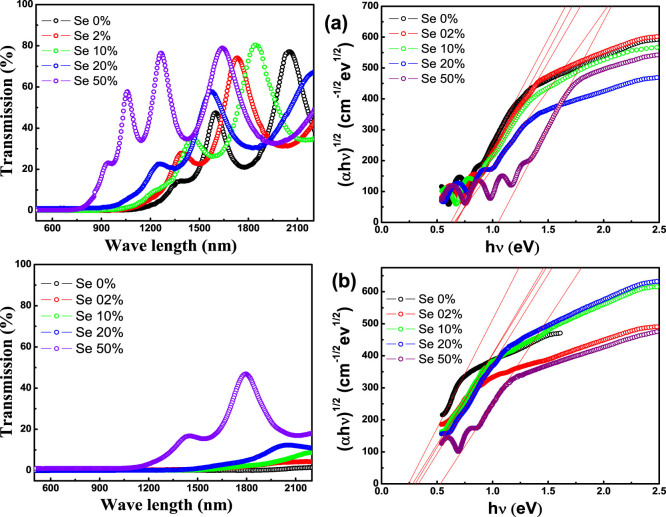
The near infrared transmittance spectra of (GST)1-xSex thin films are shown in Fig. 5. Transmittance minimum decreases with increase of Se at.% indicating the increase of band width. The spectral contribution of the absorption coefficient (α) was determined using the relation, α = (1/d)ln(I0/I) where (Io/I) is the transmittance and d is the film thickness. For higher values of (α > 104 cm−1), the absorption coefficient (α) yields the power part which obeys the Tauc31 and Davis and Mott relation32 for the allowed indirect transition:
 |
where B1/2 is the Tauc parameter, h is the Plank's constant, ν is the frequency, Eopt is the optical band gap. B1/2 refers slope in the extended region and it is the measure of disorder33. Calculated Eopt and B1/2 of GST and (GST)0.90Se0.10 films are given in Table 3.
Figure 5. Transmission spectra and the Tauc plot used for calculating the band gap of (a) AD and (b) annealed (at 300°C) (GST)1-xSex films.
Table 3. Band gap and B1/2 values of as deposited and annealed (GST)1-xSex films.
| Sample | Band gap (eV) | B1/2(cm−1/2 eV−1/2) |
|---|---|---|
| GST AD | 0.63 | 678 |
| (GST)0.98 Se0.02 AD | 0.67 | 671 |
| (GST)0.90 Se0.10 AD | 0.66 | 621 |
| (GST)0.80 Se0.20 AD | 0.64 | 492 |
| (GST)0.50 Se0.50 AD | 1.05 | 500 |
| GST 150°C | 0.38 | 699 |
| (GST)0.98 Se0.02 150°C | 0.47 | 680 |
| (GST)0.90 Se0.10 150°C | 0.50 | 646 |
| (GST)0.80 Se0.20 150°C | 0.57 | 611 |
| (GST)0.50 Se0.50 150°C | 0.71 | 520 |
| GST 300°C | 0.24 | 700 |
| (GST)0.98 Se0.02 300°C | 0.28 | 683 |
| (GST)0.90 Se0.10 300°C | 0.30 | 661 |
| (GST)0.80 Se0.20 300°C | 0.33 | 685 |
| (GST)0.50 Se0.50 300°C | 0.53 | 531 |
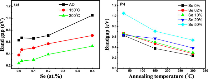
Band gap values of as deposited films varies from 0.63 eV (GST alloy) to 1.05 eV ((GST)0.50Se0.50 alloy). The widening of band gap in the amorphous phase is favorable to enhance the switching properties34. The widening of band gap in amorphous materials has fundamental importance due to the presence of trap states, which plays an important role by filling up the charge carriers to become conductive in switching. A large band gap is required to have such trap states to exist in the amorphous phase34. For films annealed at 150°C, the band gap reduced from the AD state which varies between 0.38 eV (for GST) to 0.71 eV (for (GST)0.50Se0.50). At 300°C, the band gap further reduces and varies between 0.24 eV(for GST) to 0.53 eV (for (GST)0.50Se0.50).
The optical band gap increases with the increase of Se as shown in Fig. 6(a). When the films are annealed, the band gap is found to decrease (Fig. 6(b)). The increase in band gap indicates that more energy is required for conduction to occur. In Ge10Se90-xTex, the band gap decreases with the increase of Te. The added Te substitutes Se which decreases the average cohesive energy and electronegativity35. In the present case, the added Se might increase the cohesive energy and electronegativity by forming higher energy bonds (like Ge–Se) which results in the increase of band gap.
Figure 6. (a) Variation of the band gap with Se content and (b) with annealing temperatures.
A higher value of B1/2 indicates less disorder36. B1/2 increases with annealing temperature indicating a decrease in disorder. During phase transition this defects/disorder decreases and an ordered arrangement of crystalline NaCl/hexagonal happens. Even in NaCl crystalline GST, 20% of cation sites in the Ge/Sb sub lattice are vacant and act as disorder in the system but it is less than the defects present in the amorphous phase. The addition of Se to Ge–Sb–Te induces structural changes in the system and increases the disorder in the amorphous state.
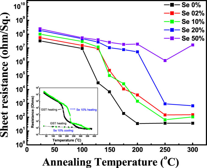
The addition Se in general increases the resistance of the as deposited films37. The change in resistance of (GST)1-xSex films with annealing temperature are shown in Fig. 7. The resistance of the GST films shows a sudden drop when annealed at 100°C. The discontinuity in resistance occurs at higher annealing temperatures for Se doped films. For the (GST)0.98Se0.02 and (GST)0.90Se0.10 films the drop in resistance is observed at 125°C. The (GST)0.80Se0.20 film shows the drop in resistance when annealed at 200°C. The change in resistance is about 5 orders of magnitude. Annealing does not have much effect on (GST)0.50Se0.50 film and change in resistance is not appreciable. The temperature dependence of resistance showed two transitions at 150°C and 240°C for GST and a single transition for (GST)0.90Se0.10 at about 200°C (see the inset of Fig. 7.)38. This is a clear evidence for increased transition temperatures and thermal stability. The in-situ resistance measurements while cooling also showed a semiconducting nature38.
Figure 7. Resistances of (GST)1-xSex measured after isothermal annealing at different temperatures.
The stronger covalent bonds due to Se doping may reduce the atomic diffusivity and hence the Tc increases for Se doped GST films39. In general, the crystallization leads to an increase in grain size and roughness9,40. For the annealed film, an increase in grain size will lead to higher conductivity due to less electron scattering at the grain boundaries. The crystallization starts initially at the free surface of the film and grows slowly and islands of crystallites nucleate homogeneously all over the film. This lead to bigger grain size formation and higher conductivity as it crystallizes.
The write current can be reduced if the electrical resistivity of the GST film in the crystalline state is increased39. A higher Tc increases the archival life time and maximum operation temperature. In present studies the Se doped GST shows a larger resistivity and increased crystallization temperature for the crystalline phase which can significantly reduce the write current and can improve the retention time of the amorphous phase.
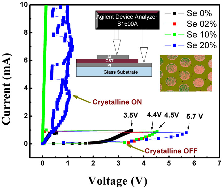
A simple device is designed and fabricated for comparing switching studies of various Se doped GST alloys. The Agilent Device Analyzer B1500A with tungsten probes was used to sweep the current and to simultaneously measure the voltage. Though the device area was large, this could give indicative (comparative) switching behaviors of undoped and Se doped GST alloys for further advanced studies.
The switching behavior of (GST)1-xSex films exhibiting memory switching are shown in Fig. 8. The highest Se content film ((GST)0.50Se0.50) does not switch under high fields. The un-doped GST switched at a threshold voltage of 3.5 V. The Se doped GST films switched at higher threshold voltages. For (GST)0.98Se0.02, (GST)0.90Se0.10 and (GST)0.80Se0.20 films switching occurs at 4.4, 4.5 and 5.7 V respectively. The added Se might preferably bond with Ge and form a Ge–Se phase30. This Ge–Se phase may have higher resistance which might push the threshold voltage to higher side. It is seen in the XRD studies that the crystallization is retarded by the Se presence and therefore the activation energy for switching. It is reported that in Si doped GST, the threshold voltage increases with Si addition39. It is found that the threshold voltage is reducing linearly with electrode separation41. So there is a possibility of reducing the set and reset voltage by reducing the volume of (GST)1-xSex device.
Figure 8. I–V switching studies of as deposited (GST)1-xSex films.
Inset show the device micrograph and schematic of the device fabricated.
Conclusions
The effect Se doping upon the phase change properties of GST has been studied. All the as deposited (GST)1-xSex films are amorphous. The (GST)1-xSex films annealed at 150°C are crystallized in NaCl structure for x ≤ 0.02. The films with 0.10 ≤ x ≤ 0.20 showed direct transition to hexagonal structure and the intermediate NaCl structure is not observed. An extra Te–Te or Te–Se layer and filling up of the vacancies in the NaCl structure of GST can possibly drive the system directly to the hexagonal structure. Resistance and thermal stability increased with the increase of Se. The overall bond energy of the system increases due to the formation Ge–Se bonds which increases the Tc. The larger resistivity of the crystalline phase in a PCM cell will be beneficial as it reduces the write current. The band gap and disorder increases with Se addition in the as deposited amorphous film and decreases in the annealed crystalline films. Band gap values of the as deposited films vary from 0.63 to 1.05 eV. The resistance contrast between the amorphous and the crystalline phases is more than 5 orders of magnitude compared to GST. Similarly, higher Tc found in these alloys is advantageous for multiple memory storage applications. These findings show that the band gap, threshold voltage and transition temperatures of GST alloys can be tuned by the addition of Se. Importantly, this study showed that the general understanding of the requirement of the metastable NaCl-like structure for the feasible phase change properties may not be correct and the direct amorphous to stable hexagonal structural transition also gives the similar kind of switching. However, crystallization kinetics of amorphous to hexagonal transition need to be studied to understand the switching speed of the Se doped GST alloys.
Methods
Sample Preparation
Thin film samples of (GST)1-xSex (x = 0, 0.02, 0.10, 0.20 and 0.50 at.%) were deposited from their bulk alloys on to glass substrates by thermal evaporation method.
Characterizations
Thickness of the films measured with a Stylus profiler (DEKTAK VEECO), was found to be 500 nm. The compositions of the deposited films were verified with Energy-dispersive X-ray spectroscopy. Films were annealed at selected temperatures for 1 h at a vacuum of 10−5 mbar using a resistive heater in a vacuum chamber. The annealed films were subjected to X-ray diffraction (XRD) to identify the crystalline structures with CuKα radiation (λ = 1.54 Å) in a BRUKER D8 ADVANCE diffractometer. Transmission spectra of the films were taken in the VIS-NIR range (550–2200 nm) using PerkinElmer Lambda 750 VIS-NIR Spectrometer. Raman spectroscopy (LabRAM HR system) measurements were performed using 514.5 nm Argon laser with a charge coupled device detector in backscattering geometry with a spectral resolution of 0.5 cm−1. The power with the filter is 0.01 mW on the sample and the accumulation time for each spectrum is 180 seconds, which did not induce any crystallization. Various laser power-filter combinations have been tried to reduce the laser induced crystallisation on the sample surface. Filter D0.3 with laser set power represents power/2, filter D1 gives power/10 and filter D2 gives power/100. Electrical switching studies have been performed using a probe station with Agilent Device Analyzer B1500A. The active area of the device was 376 μm2 in a vertical sandwich geometry of Pt (100 nm)/PCM (500 nm)/Al (300 nm) on glass substrates. Current was swept between upper Al electrode and lower Pt electrodes and the corresponding voltages were measured. Two probe resistance measurements were carried out using the same Agilent Device Analyzer on the samples annealed at different temperatures. Each reading is an average of three measurements.
Author Contributions
E.M.V. conducted the experiments and wrote the main manuscript text under K.S.S. guidance. K.R. edited and suggested some modifications. All authors reviewed the manuscript.
Acknowledgments
The authors thank Department of Science and Technology, India for the financial support and Micro and Nano Characterization Facility (MNCF) at the Centre for Nano Science and Engineering (CeNSE), Indian Institute of Science, Bangalore, India.
References
- Shportko K. et al. Resonant bonding in crystalline phase-change materials. Nat. Mater. 7, 65–658 (2008). [DOI] [PubMed] [Google Scholar]
- Ovshinsky S. R. Reversible Electrical Switching Phenomena in Disordered Structures, Physical Review Letters. Phys. Rev. Lett. 21, 1450 (1968). [Google Scholar]
- Tomforde J. et al. The influence of Se doping upon the phase change characteristics of GeSb2Te4, Solid State Sciences. Solid State Sci. 11, 683–687 (2009). [Google Scholar]
- Matsunaga T., Yamada N. & Kubota Y. Structures of stable and metastable Ge2Sb2Te5, an intermetallic compound in GeTe–Sb2Te3 pseudobinary systems. Acta Crystallogr., Sect. B. 60, 685–691 (2004). [DOI] [PubMed] [Google Scholar]
- Lu Y. et al. Ga–Sb–Se material for low-power phase change memory. Appl. Phys. Lett. 99, 243111 (2011). [Google Scholar]
- Yoon S.-M. et al. Sb-Se-based phase-change memory device with lower power and higher speed operations. IEEE Electron Device L. 27, 445–447 (2006). [Google Scholar]
- Friedrich I., Weidenhof V., Njoroge W., Franz P. & Wuttig M. Structural transformations of Ge2Sb2Te5 films studied by electrical resistance measurements. J. Appl. Phys. 87, 4130 (2000). [Google Scholar]
- Mendoza-Galván A. & González-Hernández J. Drude-like behavior of Ge:Sb:Te alloys in the infrared. J. Appl. Phys. 87, 760 (2000). [Google Scholar]
- Song K. H., Kim S. W., Seo J. H. & Lee H. Y. Characteristics of amorphous Ag0.1(Ge2Sb2Te5)0.9 thin film and its ultrafast crystallization. J. Appl. Phys. 104, 103516 (2008). [Google Scholar]
- Yamada N. & Matsunaga T. Structure of laser-crystallized Ge2Sb2Te5 sputtered thin films for use in optical memory. J. Appl. Phys. 88, 7020 (2000). [Google Scholar]
- Kolobov A. V. et al. Understanding the phase-change mechanism of rewritable optical media. Nat. Mater. 3, 703–708 (2004). [DOI] [PubMed] [Google Scholar]
- Sun Z., Zhou J. & Ahuja R. Structure of Phase Change Materials for Data Storage. Phys. Rev. Lett. 96, 055507 (2006). [DOI] [PubMed] [Google Scholar]
- Vinod E. M., Naik R., Ganesan R. & Sangunni K. S. Signatures of Ge2Sb2Te5 film at structural transitions. J. Non-Cryst. Solids 358, 2927–2930 (2012). [Google Scholar]
- Privitera S. et al. Crystallization and phase separation in Ge2+xSb2Te5 thin films. J. Appl. Phys. 94, 4409 (2003). [Google Scholar]
- Wang K., Steimer C., Wamwangi D., Ziegler S. & Wuttig M. Effect of indium doping on Ge2Sb2Te5 thin films for phase-change optical storage. Appl. Phys. A 80, 1611–1616 (2005). [Google Scholar]
- Phillips J. C. & Thorpe M. F. Constraint theory, vector percolation and glass formation. Solid State Commun. 53, 699–702 (1985). [Google Scholar]
- Narayanan R. A., Asokan S. & Kumar A. Evidence concerning the effect of topology on electrical switching in chalcogenide network glasses. Phys. Rev. B. 54, 4413 (1996). [DOI] [PubMed] [Google Scholar]
- Song S. A., Zhang W., Sik Jeong H., Kim J.-G. & Kim Y.-J. In situ dynamic HR-TEM and EELS study on phase transitions of Ge2Sb2Te5 chalcogenides. Ultramicroscopy 108, 1408–1419 (2008). [DOI] [PubMed] [Google Scholar]
- Yamada N. Origin, secret, and application of the ideal phase-change material GeSbTe. Phys. Status Solidi B. 249, 1837–1842 (2012). [Google Scholar]
- Cho E., Yoon S., Yoon H. R. & Jo W. Micro-Raman Scattering Studies of Ge–Sb–Te Bulk Crystals and Nanoparticles. J. Korean Phys. Soc. 48, 1616–1619 (2006). [Google Scholar]
- Liu Bo, Zhi-Tang S., Ting Z., Song-Lin F. & Bomy C. Raman spectra and XPS studies of phase changes in Ge2Sb2Te5 films. Chinese Phys. 13, 1947–1950 (2004). [Google Scholar]
- Andrikopoulos K. S., Yannopoulos S. N., Kolobov A. V., Fons P. & Tominaga J. Raman scattering study of GeTe and Ge2Sb2Te5 phase-change materials. J. Phys. Chem. Solids 68, 1074–1078 (2007). [Google Scholar]
- Nemec P. et al. Ge–Sb–Te thin films deposited by pulsed laser: An ellipsometry and Raman scattering spectroscopy study. J. Appl. Phys. 106, 103509 (2009). [Google Scholar]
- Tominaga J. & Atoda N. Study of the Crystallization of GeSbTe Films by Raman Spectroscopy. Jpn. J. Appl. Phys. 38, L322–L323 (1999). [Google Scholar]
- Sosso G. C., Caravati S., Mazzarello R. & Bernasconi M. Raman spectra of cubic and amorphous Ge2Sb2Te5 from first principles. Phys. Rev. B. 83, 134201 (2011). [DOI] [PubMed] [Google Scholar]
- De Bastiani R. et al. Crystallization of ion amorphized Ge2Sb2Te5 thin films in presence of cubic or hexagonal phase. J. Appl. Phys. 107, 113521 (2010). [Google Scholar]
- Sergey K., Kudoyarova V., Nguyen H. P., Smirnov A. & Lebedev V. Influence of doping on the structure and optical characteristics of Ge2Sb2Te5 amorphous films. phys. status solidi (c) 8, 2688–2691 (2011). [Google Scholar]
- Tronc P., Bensoussan M., Brenac A. & Sebenne C. Optical-Absorption Edge and Raman Scattering in GexSe1-x Glasses. Phys. Rev. B. 8, 5947 (1973). [Google Scholar]
- Sugai S. Stochastic random network model in Ge and Si chalcogenide glasses. Phys. Rev. B. 35, 1345 (1987) [DOI] [PubMed] [Google Scholar]
- Vinod E. M., Singh A. K., Ganesan R. & Sangunni K. S. Effect of selenium addition on the GeTe phase change memory alloys. J. Alloys Compd. 537, 127–132 (2012). [Google Scholar]
- Tauc J., Grigorov R. & Vancu A. Optical properties and electronic structure of amorphous Germanium. Phys. Status Solidi 15, 627–637 (1966). [Google Scholar]
- Davis E. A. & Mott N. F. Conduction in non-crystalline systems V. Conductivity, optical absorption and photoconductivity in amorphous semiconductors. Philos. Mag. 22, 903–922 (1970). [Google Scholar]
- Vinod E. M., Naik R., Faiyas A. P. A., Ganesan R. & Sangunni K. S. Temperature dependent optical constants of amorphous Ge2Sb2Te5 thin films. J. Non-Cryst. Solids 356, 2172–2174 (2010). [Google Scholar]
- Welnic W. et al. Unravelling the interplay of local structure and physical properties in phase-change materials. Nat. Mater 5, 56–62 (2006). [Google Scholar]
- Sharma P. & Katyal S. C. Effect of tellurium addition on the physical properties of germanium selenide glassy semiconductors. Physica B: Condensed Matter 403, 3667–3671(2008). [Google Scholar]
- Zanatta A. R. & Chambouleyron I. Absorption edge, band tails, and disorder of amorphous semiconductors. Phys. Rev. B. 53, 3833 (1996). [DOI] [PubMed] [Google Scholar]
- Vinod E. M. & Sangunni K. S. The effect of Se doping on spectroscopic and electrical properties of GeTe. Thin Solid Films 550, 569–574 (2014). [Google Scholar]
- Vinod E. M., Ramesh K., Ganesan R. & Sangunni K. S. Direct hexagonal transition of amorphous (Ge2Sb2Te5)0.9Se0.1 thin films. Appl. Phys. Lett. 104, 063505 (2014). [Google Scholar]
- Bao-Wei Q. et al. Improvement of Electrical Properties of the Ge2Sb2Te5 Film by Doping Si for Phase Change Random Access Memory. Chinese Phys. Lett. 23, 172 (2006). [Google Scholar]
- Shin M.-J. et al. Chemical Bonding Characteristics of Ge2Sb2Te5 for Thin Films. J. Korean Phys. Soc. 44, 10–13 (2004). [Google Scholar]
- Xiong F., Liao A. D., Estrada D. & Pop E. Low-Power Switching of Phase-Change Materials with Carbon Nanotube Electrodes. Science 332, 568–570 (2011). [DOI] [PubMed] [Google Scholar]


