Abstract

A series of In2O3 thin films, ranging from X-ray diffraction amorphous to highly crystalline, were grown on amorphous silica substrates using pulsed laser deposition by varying the film growth temperature. The amorphous-to-crystalline transition and the structure of amorphous In2O3 were investigated by grazing angle X-ray diffraction (GIXRD), Hall transport measurement, high resolution transmission electron microscopy (HRTEM), electron diffraction, extended X-ray absorption fine structure (EXAFS), and ab initio molecular dynamics (MD) liquid-quench simulation. On the basis of excellent agreement between the EXAFS and MD results, a model of the amorphous oxide structure as a network of InOx polyhedra was constructed. Mechanisms for the transport properties observed in the crystalline, amorphous-to-crystalline, and amorphous deposition regions are presented, highlighting a unique structure–property relationship.
Introduction
Fundamental understanding of the chemical and structural origins of transparent conducting oxides (TCOs) has allowed TCOs to evolve into important materials for photovoltaic devices and optoelectronic applications.1−4 Transparent oxide semiconductors (TOSs) are currently being explored as thin film transistor (TFT) materials, as an enabling technology for the next generation of computing, communication, and identification devices.3,5 Initially, the technological application of TCOs and TOSs employed these materials in their crystalline form. There is, however, an increasing shift toward the use of these materials in their amorphous form. In 2010, an estimated 30–40% of all flat panel displays employed an amorphous TCO material.6
Amorphous TCOs and TOSs (a-TCOs and a-TOSs) have several advantages over their crystalline counterparts. In general, amorphous materials are deposited at lower temperatures7 which tend to simplify the deposition process and expand the number of substrates the material can be deposited on, such as plastics. Amorphous materials lack grain boundaries and are isotropic and, hence, tend to etch more uniformly,8−10 have lower surface roughness,11,12 and can be deposited uniformly over large areas.8,13 Some amorphous materials can also be less prone to fracture, hence being more pliable, lending themselves to the possibility of flexible electronics.8,14 These advantages are realized without a significant loss to the seminal properties of conductivity and transparency, for optimized materials.15
The electrical and optical properties of crystalline TCOs and TOSs (c-TCOs and c-TOSs) are strongly influenced by the oxygen content of the film;16 the same is true for a-TCOs and a-TOSs.17 For c-TCOs and c-TOSs, their properties are also affected by factors related to the crystal structure such as grain size18 and crystallographic direction.19 By understanding how structure affects properties, it has been possible to improve the performance of c-TCOs and c-TOSs. An understanding of the structure in a-TCOs and a-TOSs would afford the same opportunity for materials optimization. There is, however, a much smaller knowledge base as to the structure of a-TCOs and a-TOSs than for their crystalline counterparts.
The basic structure for TCOs and TOSs is a network of MOx polyhedra. Each metal ion is coordinated with some number of oxygen ions, known as the M–O coordination number (NM–O), at some bond distance or distances, known as the M–O bond-distance (RM–O), to form polyhedra. The polyhedra are then linked together either at their corners, sharing one oxygen between two polyhedra (corner-sharing polyhedra); at their edges, sharing two oxygen between two polyhedra (edge-sharing polyhedra); or, much less common, along their faces, sharing three or more oxygen between polyhedra (face-sharing polyhedra), see Figure 1. The linking of polyhedra results in the formation of a network where, ignoring the interposing oxygen for the moment, each metal ion is coordinated with some number of other metal ions, the M–M′ coordination number (NM–M′), at some distance or distances, the M–M′ distance (RM–M′). Here M and M′ are used since in multication materials a specific cation can be coordinated with a multiplicity of other cation species. The fact that there is an interposing oxygen between cations leads to the concept of a M–O–M′ bond angle. In discussing the structure of a TCO or TOS, one looks at both the polyhedra structure (NM–O and RM–O) and the network formed by the linked polyhedra (NM–M′, RM–M′, and the M–O–M′ bond angle). It is the distortions in the MOx polyhedra and integration of the polyhedra into a continuous network that ultimately govern the properties of the oxides.
Figure 1.
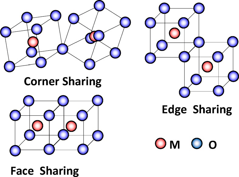
Corner, edge, and face sharing polyhedra.
The crystalline structure for many of the indium oxide based TCOs and TOSs is that of indium oxide, In2O3 (IO), bixbyite structure (space group Ia3, number 206). Bixbyite is a fluorite-type structure with one-quarter of the anions missing; a periodic structure that produces “structural vacancies.” In the crystalline structure, the oxygen atoms are octahedrally coordinated around indium; all indium cations are surrounded by six oxygen atoms (c-NIn–O = 6) and two structural vacancies. This is also known as the first-shell around indium. The structural vacancy positions can sit along the body diagonal (b-site) or along a face diagonal (d-site), Figure 2. The b-site represents 25% of the octahedra arrangement and the d-site 75% of the octahedra arrangement. In the b-site arrangement, all the oxygens are equidistant from the indium at 2.18 Å. In the d-site arrangement, there are two oxygens at each distance 2.13, 2.19, and 2.23 Å. The average In–O bond distance for all arrangements in the theoretical structure is 2.18 Å (c-RIn–O = 2.18 Å). The existence of structural vacancies gives rise to two configurations by which InO6 octahedra link together in crystalline In2O3: In the first, both an oxygen and a structural vacancy are shared between adjacent polyhedra with the end result that the polyhedral are only joined at a corner, hence “corner sharing;” in the second, two oxygens are shared between the adjacent polyhedra with the end result that the polyhedra are joined along the entire edge, “edge sharing,” Figure 2. This leads to two distinct sets of adjacent polyhedra In–In neighbors: There are six-adjacent edge-sharing polyhedra, NIn–In = 6, at a distance of ∼3.34 Å, RIn–In = 3.34 Å, and six-adjacent corner-sharing polyhedra, NIn–In* = 6, at a distance of ∼3.83 Å, RIn–In* = 3.83 Å. These make up the second and third shells around indium, respectively, the first shell being the InO6 octahedra.
Figure 2.
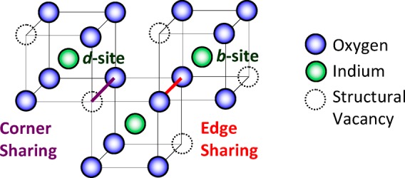
Structure of crystalline In2O3 (bixbyite).
A common method of probing the structure of these materials is extended X-ray absorption fine structure (EXAFS).20 Fourier transform analysis of the EXAFS data yields structural information in the vicinity of each kind of atom whose absorption is probed. This information can include M–O and M–M′ coordination numbers (N) and bond distances (R) as well as the statistical spread of bond distances (σ2) due to thermal motion and/or static disorder; this last factor is of particular interest in amorphous materials.21 As mentioned, in materials built up of MOx polyhedra, the M–O structure is often referred to as the first shell and the nearest M–M′ structure as the second shell. In the first shell, there are no multiple scattering effects, and the interpretation of data is fairly straightforward even in multiple cation systems. Interpretation for data in the second shell where multiple scattering effects can occur is complex, particularly in multiple cation systems. The interpretation of the second shell becomes more complex in amorphous systems where the second shell is less well ordered; the third shell is even harder to interpret.
Several EXAFS studies have been done on the structures of In, Ga, Sn, and Zn containing a-TCOs and a-TOSs. These studies are summarized in the Supporting Information. All but one deal exclusively with the first shell, that is, the coordination of oxygen around the metal cations. Similarly, available theoretical models of amorphous oxides derived from molecular dynamics simulations focus primarily on the first shell M–O results with no or limited information on the M–M distances and coordination.22−30 The coordination of oxygen around indium is frequently compared to that of crystalline indium oxide (bixbyite), a c-NIn–O of 6 and c-RIn–O of 2.18 Å. With the exception of the studies by Cho et al., there is general agreement that in the amorphous materials RIn–O is contracted relative to that found in the crystalline material. There is, however, little agreement in NIn–O, which ranges from a low of 4.5 to a high of 6.1. Differences in the chemical environments for the different materials might contribute to the large spread of values for NIn–O; however, even for compositionally equivalent materials, such as InGaZnO4 where NIn–O ranges from 4.5 to 5.8 and Zn0.3In1.4Sn0.3O7 where NIn–O ranges from 5 to 6 (albeit set), there is little agreement. Although these differences may be due, in part, to differences in processing methods, the complexities encountered when modeling multication systems make it possible to obtain different results from the same data depending on the simplifying assumptions and modeling parameters used. These difficulties in data interpretation are greatly compounded for the second shell where multiscattering effects and the suppression of the Fourier transform at the higher R-range require additional simplifying assumptions.
Although pure indium oxide (IO) is rarely used in technological applications, it is the progenitor of many TCO and TOS systems. In structural studies like these, IO has the advantage over more complex systems in that fewer constraints and assumptions need to be imposed when modeling the data. For this study, a series of IO films, 350 nm thick, were grown by pulsed laser deposition (PLD) at temperatures ranging from −100 to 600 °C in order to determine variations in the structural characteristics and to relate those to the optimum properties. X-ray absorption spectroscopy and EXAFS analysis were performed on these samples to determine the indium–oxygen coordination number (NIn–O) and the average indium–oxygen bond distance (RIn–O), as well as the statistical spread of the bond distance (σ2In–O). Additionally the next-nearest neighbor indium–indium coordination number (NIn–In) and the bond distance (RIn–In), as well as the statistical spread of the bond distance (σ2In–In), were determined.
A powerful model for the construction of a plausible structure of an amorphous material is molecular dynamics (MD) liquid-quench simulations. In a liquid-quench simulation, a crystalline structure is heated to several thousand degrees for mixing. The equilibrium melt is then cooled rapidly (quenched) in a stepwise fashion to a final temperature; different total quench times are realized by changing the quench rate. In some simulations, the cooled structure is allowed to relax at constant volume to an energy-minimized quenched structure. PLD is a physical analogue to a liquid-quench simulation. In PLD, a crystalline target is heated to several thousand degrees by a laser pulse. The plasma plume is rapidly cooled to a solid structure at the substrate. The structure then relaxes, to some extent, to a local energy minimum. The results of these experiments, therefore, readily lend themselves to interpretation by MD liquid-quench simulations. In this work, first-principles density-functional-based molecular dynamics is employed to obtain a-IO structures at different quench rates in order to understand their effect on the structural properties of a-IO and to explain the experimentally observed trends in PLD-grown samples. With the aid of MD simulations, it was possible not only to corroborate the first and second shell results by EXAFS but also to extract additional information for the third-shell structure of a-IO.
Experimental Section
IO thin-films, ∼350 nm thick, were grown by PLD from a dense hot-pressed In2O3 target (25 mm diameter). PLD was accomplished with a 248 nm KrF excimer laser with a 25 ns pulse duration and operated at 2 Hz. The 200 mJ/pulse beam was focused onto a 1 mm × 3 mm spot size. The target was rotated at 5 rpm about its axis to prevent localized heating. The target–substrate separation was fixed at 10 cm. The films were grown on fused-silica substrates in an O2 ambient of 8 mTorr. The substrates were attached to the substrate holder with silver paint. For films grown above room temperature, a resistively heated substrate holder was used; for films grown below room temperature, a liquid nitrogen cooled substrate holder was used.
Sheet resistance (Rs: Ω/□), carrier type, area carrier concentration (na: 1/cm2), and carrier mobility (μH: cm2/V·s) were measured with an Ecopia 3000 Hall measurement system on samples in the van der Pauw geometry. Carrier density (nv: 1/cm3) and resistivity (ρ: Ω·cm) were calculated by dividing the area carrier concentration and sheet resistance, respectively, by the film thickness. Film thickness (d: nm) was measured using a spectral reflectometer (Filmetrics F20). Grazing incidence X-ray diffraction (GIXRD) was performed using an 18 kW Rigaku ATX-G diffractometer. Cu Kα radiation (λ = 1.54 Å) was conditioned by a parabolic multilayer mirror and collimated to produce a 0.1 mm (vertical) by 5 mm (horizontal) beam with an incident flux of ∼2 × 10⁸ photons/s; a beam incident angle of 0.46° was used. Film composition was measured by X-ray Photoelectron Spectroscopy (XPS) using a Thermo Scientific ESCALAB 250Xi using a Al Kα source and a takeoff angle of 90°. An argon ion source was used to clean carbon from the surface prior to analysis. The flood gun was used on all analysis although it was only needed on the more insulating samples to maintain charge neutrality.
X-ray absorption spectroscopy (XAS) was performed at the 5-BMD beamline of DND-CAT at the Advanced Photon Source (APS) of Argonne National Laboratory (Argonne, IL). The In Kα fluorescence emissions from the indium oxide thin films were measured using a four-element Si-drifted detector (SII) with the incident X-ray angle θ at about 45° with respect to the sample surface. The XAS data were analyzed with the ATHENA software packages.31 The data were Fourier transformed with a Hanning window over multiple k ranges where one-shell and three-shell fits were examined; see the Supporting Information for a detailed analysis of the rationale behind the choice of fit parameters. The k-range of the EXAFS data used in the analyses was k = 2.24–12.67 Å–1 with a k-weight of 2. Fitting carried out in R space was from R = 1.0 to 2.0 Å for the one-shell model and R = 1.0 to 4.0 Å for the three-shell model. Paths for the first (In–O), second (In–In), and third (In–In*) were used in the three-shell model; only the first shell was used in the one-shell model.
For transmission electron microscopy (TEM), the IO films were mechanically cleaved from the substrate and deposited onto a holey carbon grid. The samples were studied using a Jeol ARM 200F microscope operated at 200 keV. In order to prevent crystallization by the electron beam, the samples were examined under low electron-dose illumination using the smallest condenser lens aperture (10 μm). In this way, the same illumination conditions were used for selected area electron diffraction (SAED) patterns taken with a beam current ranging between 5 and 15 pA/cm2, and patterns were collected at exposure times of 10 to 20 s.
Theoretical
The amorphous In–O structures were generated using first-principles molecular dynamics as implemented in the Vienna Ab Initio Simulation package.32−35 These calculations are based on the density functional theory (DFT) within generalized gradient approximation (GGA) with the PBE functional.36 For initial structure, bixbyite In2O3 supercells containing 80, 130, or 180 atoms and with a density of 7.12 g/cm3 were used. To remove the memory of the atomic arrangement, the initial structure was melted at 3000 K for 6 ps. Next, the melt was cooled to 2200–1700 K at the rate of 100 K/1.2 ps and then rapidly quenched to 100 K using different quench rates ranging from 700 K/ps to 5 K/ps. In order to make these challenging calculations computationally efficient, a low cutoff of 260 eV was used and k-point sampling was restricted to the Γ point only. The final structures were equilibrated at 300 K for 6 ps with a cutoff of 400 eV. All simulations were carried out within the NVT ensemble with a Nosé–Hoover thermostat using an integration time step of 2 fs. For the amorphous structures with different supercell sizes, we analyzed the pair distribution functions and found that an 80-atom supercell is sufficient to describe the amorphous character, as found in previous theoretical calculations.23
We note here that a typical cooling rate employed in ab initio MD simulations of amorphous oxides is 200–100 K/ps; slower cooling rates in DFT-based MD require significant computational efforts and were not previously reported for amorphous oxide semiconductors (in contrast to classical MD simulations). These quench rates were shown to produce reliable amorphous structures.23,24,37−39 Indeed, simple estimations based on the thermal conductivity, heat capacity, and density of In2O3 suggest that a time of 10–12 to 10–13 s is required to cool a 1 nm thick oxide by 1 K. In this work, cooling rates ranging from ∼700 K/ps to 5 K/ps are employed to compare the MD simulation results to the experimentally observed dependence of the structural properties on the PLD deposition temperature. The agreement between EXAFS and MD results helps explain the intriguing behavior of mobility near the crystalline–amorphous transition. Additionally, the results of the MD simulations are used to apply reasonable constraints on the EXAFS analysis of the second and third shells.
Results and Discussion
For many thin-film material systems, the transition between amorphous and crystalline can be accomplished by changing the temperature of deposition; the crystalline phase being favored by higher deposition temperatures. Such is the case for IO deposited on fused quartz by PLD. Figure 3 is the GIXRD patterns of IO films ∼350 nm thick. Films grown at temperatures of 0 °C and below are all X-ray diffraction amorphous (a-IO). The first sign of crystallinity is observed at +25 °C. The GIXRD spectra for the crystalline films (c-IO) are typical of that observed for polycrystalline bixbyite In2O3.
Figure 3.
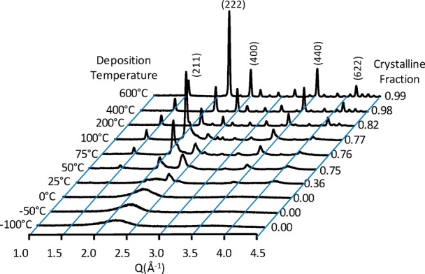
GIXRD patterns of indium oxide films, ∼350 nm thick, as a function of deposition temperature. The c-IO/a-IO ratio, is determined by the area of the crystalline XRD peaks to the combined areas of the crystalline XRD peaks and the “amorphous hump.”
The films deposited at 0 °C and below have been referred to as “X-ray diffraction amorphous” rather than simply amorphous because they can still contain nanocrystalline inclusions. At deposition temperatures as low as −50 °C, nanocrystalline inclusions, 1.9 to 2.4 nm in size, can be found in a dominant amorphous phase as seen in the HRTEM image of Figure 4a; the SAED inset confirms the presence of a dominant amorphous phase. As the deposition temperature is increased to 0 °C, the size of the nanocrystalline inclusions increases to between 2.2 and 3.4 nm; the amorphous phase is still dominant, Figure 4b. At a deposition temperature of +100 °C, where crystallinity is clearly visible by X-ray diffraction, the crystals are quite large and more dominant as evidenced in Figure 4c where the inset SAED pattern has begun to form diffraction reflections which are closer in appearance to a highly crystalline sample, Figure 4d, than the amorphous samples, Figure 4a and b. Although nanocrystalline inclusions exist in the diffraction amorphous films, to simplify notation, for the remainder of the paper the diffraction amorphous films will simply be referred to as amorphous and the advent of crystallinity to occur at +25 °C where it is first observable by X-ray diffraction.
Figure 4.
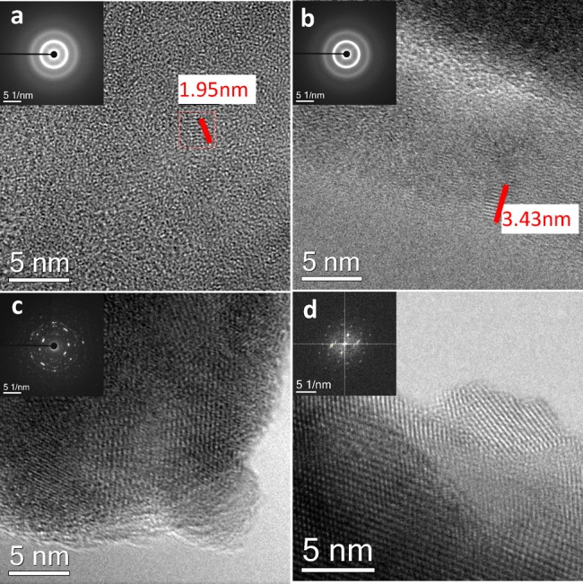
HRTEM images of indium oxide films deposited at (a) −50 °C, (b) 0 °C, (c) +100 °C, and (d) +600 °C. Insets are representative SAED patterns from the respective films.
One of the main objectives for the study of structure is to optimize properties; for TCOs and TOSs one property of major interest is carrier mobility (μH). Figure 5 shows the Hall carrier mobility of the 350 nm films as a function of growth temperature. In the high temperature c-IO region (+400 to +600 °C), μH is high (60–70 cm2/V·s), typical of highly crystalline (albeit polycrystalline) films. The value of μH is again quite high (∼60 cm2/V·s) right at the advent of crystallinity (0 °C to +25 °C); the possible origins of this high mobility will be explored in the EXAFS analysis and MD simulations sections. The mobility decreases between −25 °C and −100 °C and reasons for this will also be explored in the EXAFS analysis and MD simulations sections. The region between the a-IO and c-IO films has a decrease in mobility from that observed for both the films deposited in the high temperature crystalline region (≥400 °C) and the films deposited right at the advent of crystallinity (0 to 25 °C). This region contains both crystalline and amorphous material in sufficient quantities to be detectable by X-ray diffraction; incoherent boundaries between the crystalline and amorphous phases can serve as scattering centers. As the first crystallites form in a majority amorphous phase, they act as scattering centers that lower the mobility; further increase in deposition temperature increases the number of crystalline scattering centers attended by further decrease in mobility until the crystalline phase becomes the major percolation path through the material. At this point, the amorphous regions become the de facto scattering centers. A further increase in temperature decreases the amorphous fraction, thereby decreasing the number of scattering centers and increasing mobility.
Figure 5.
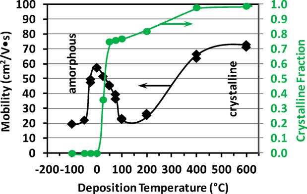
Hall mobility of indium oxide films, ∼350 nm thick, as a function of deposition temperature.
XAS and EXAFS analysis was performed on the same samples to gain greater insight into the differences in film structure. The In–O coordination numbers are shown in Figure 6a. The highly crystalline samples have 6-fold oxygen-coordination around indium (c-NIn–O ∼ 6) consistent with the bixbyite structure. The fully amorphous films have significantly lower oxygen-coordination around indium (a-NIn–O ∼ 5.3). Two possible reasons for the lower oxygen coordination are a difference in stoichiometry or a change in structure. XPS was used to compare the composition of a similar set of thinner (65 nm) films deposited over the same temperature range (−100 to 600 °C); all the films had the same In/O ratio within ±5% with no observable trend with respect to deposition temperature. Hence, a change in structure is the more plausible explanation for the change in NIn–O.
Figure 6.
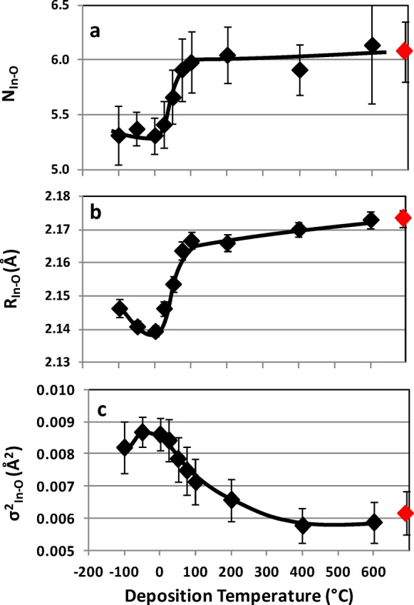
(a) In–O coordination number, NIn–O, (b) In–O bond distance, RIn–O, and (c) σ2In–O for the In–O shell of indium oxide films, ∼350 nm thick, as a function of deposition temperature: Red markers, powdered In2O3 standard.
The In–O bond distance for the highly crystalline samples is, on the average, ∼2.17 Å (RIn–O = 2.17 Å), Figure 6b, just slightly less than the ideal structural distance of 2.18 Å. There is a further contraction in the average In–O bond distance in the amorphous films. This is consistent with a reduced coordination number observed in the amorphous films; lower oxygen coordination also allows a reduction in In–O distance while maintaining O–O separation. The minimum at 0 °C, ∼2.14 Å, is interesting in that it also corresponds to the highest temperature at which an amorphous film can be grown and the point of highest carrier mobility. However, because of the relatively small variation in RIn–O for the amorphous samples additional measurements would be needed to confirm a minimum. The statistical spread of bond distances (σ2In–O) due to thermal motion and/or static disorder ranges from a low of ∼0.0054 Å2 to a high of ∼0.0085 Å2, Figure 6c. As might be expected, the lowest σ2In–O corresponds to the highly crystalline films deposited at 400 and 600 °C, and the highest σ2In–O to the amorphous films.
To achieve an amorphous structure, the regularity of the crystalline structure, Figure 7a, must be perturbed, usually in bond distance and/or bond angle. If, for the moment, the polyhedra are assumed relatively undistorted, the structure can still become amorphous by virtue of distortions in the way the polyhedra are linked. Consider what happens when the In–O–In bond angle is changed by the rotation of the polyhedra edges about an oxygen. If the rotation occurs between corner-sharing polyhedra, Figure 7b, the net effect is to change the In–In bond distance as well as the In–O–In bond angle. If the rotation occurs between edge-sharing polyhedra, Figure 7c, the net effect is not only to change the In–O–In bond angle and In–In bond distance but to also require the introduction of an additional structural vacancy thus lowering the In–O coordination number by an average of 1/2 for the two polyhedra involved, Figure 7c; the polyhedra will also change from being edge-sharing to corner-sharing. A second way the In–O coordination number could be lowered is by rotating the polyhedra along an edge thereby disjoining adjacent polyhedra; the separation of corner-sharing polyhedra would result in lowering the In–O coordination number by an average of 1/2 for the two polyhedra involved, Figure 8b, and the separation of edge-sharing polyhedra would result in lowering the In–O coordination number by an average of 1 for the two polyhedra involved, Figure 8c. The caricatures of the rotations in Figures 7 and 8 are greatly simplified. In the crystalline solid, the polyhedra are linked over large volumes; when a polyhedron is rotated, the bonds with all adjacent polyhedra are perturbed which are, in turn, displaced within the lattice network. The net effect, if stoichiometry is maintained, is to reduce NIn–O.
Figure 7.
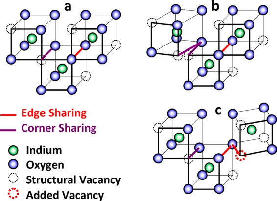
(a) Unperturbed lattice; (b) rotation of corner sharing polyhedra; (c) rotation of edge sharing polyhedra.
Figure 8.
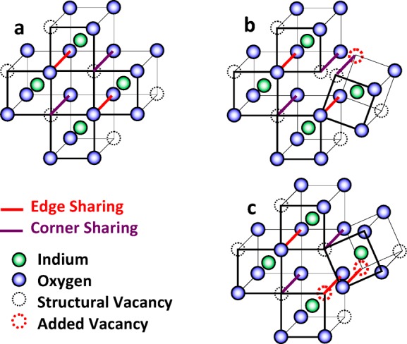
(a) Unperturbed lattice; (b) breaking of corner sharing bond; (c) breaking of edge sharing bond.
For c-IO, the second shell is made up of the six-adjacent edge-sharing polyhedra, NIn–In = 6, at a distance of RIn–In ∼ 3.34 Å. The highly crystalline samples, 400 and 600 °C, have 6-fold nearest-neighbor In−In coordination (c-NIn–In ∼ 6) consistent with the number of edge-sharing nearest-neighbor polyhedra in the bulk bixbyite structure. The fully amorphous films have significantly lower nearest-neighbor In−In coordination (a-NIn–In ∼ 2), Figure 9a. For the highly crystalline films, the nearest-neighbor In−In distance is, on the average, 3.36 Å (c-RIn–In ∼ 3.36 Å), slightly larger than the value for the ideal bixbyite structure. This decreases to a minimum of 3.29 Å for the fully amorphous sample grown at 0 °C (a-RIn–In ∼ 3.31 Å), Figure 9b. Again, the minimum bond distance is observed at the point of highest mobility. The statistical spread of In–In bond distances (σ2In–In) due to thermal motion and/or static disorder ranges from a low of ∼0.004 Å2 to a high of ∼0.014 Å2, Figure 9c. As might be expected, the lowest statistical spread corresponds to the highly crystalline films deposited at 400 and 600 °C; the highest statistical spread to the amorphous samples.
Figure 9.
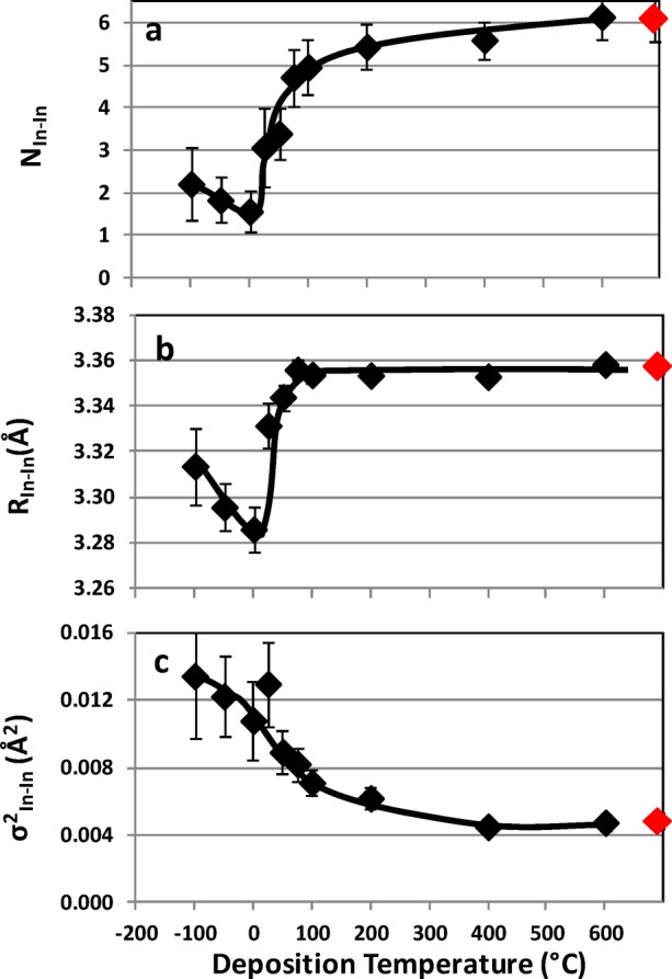
(a) In–In coordination number, NIn–In; (b) In–In bond distance, RIn–In; and (c) σ2 for the In–In shell, σ2In–In, of indium oxide films, ∼350 nm thick, as a function of deposition temperature: Red markers, powdered In2O3 standard.
The decrease in NIn–In is consistent with the mechanism proposed for the decrease in NIn–O. The rotation pictured in Figure 7c would convert two edge-shared second-shell polyhedra into two corner-shared third-shell polyhedra while increasing the number of structural oxygen vacancies by only 1. A similar effect has been observed in quartz where crystalline quartz was observed to have c-NSi–O ∼ 4.0 and c-NSi–Si ∼ 4.0 while fused silica was observed to have a-NSi–O ∼ 3.7 and a-NSi–Si ∼ 1.1.40 The rotation in the In–O–In bond angle can also account for the decrease in RIn–In. The second shell bond distance, RIn–In, is more or less a maximum in the crystalline structure; therefore, RIn–In would be expected to decrease in the amorphous phase and be attended by an increase in σ2In–In. A decrease in RIn–In increases the In–In bond orbital overlap, which would contribute to higher mobility. The decrease in mobility with a further decrease in deposition temperature from 0 °C is attended by an increase in RIn–In. Here, we believe the lattice is frozen in a less relaxed state before polyhedra can rotate into closer proximity. X-ray reflectivity studies on thinner films (60 nm thick) indicate as the deposition temperature is lowered below the point at which the films become X-ray diffraction amorphous the density of the films decrease;41 this would be consistent with a more open structure being frozen in place.
The analysis of the third shell, the structure of the corner shared polyhedra, is more difficult to determine; even for the highly crystalline samples the calculated third-shell coordination number is ∼5 (c-NIn–In* ≈ 5), see the Supporting Information. There is, however, a piori knowledge that this value should be ∼6 because of the highly crystalline nature of the samples. When the value of NIn–In* is constrained in the model to 6, the computed value for the third-shell neighbor distance is 3.84 Å, with a statistical spread of 0.006 Å2. The calculated bond distance is just slightly larger than the value of 3.83 Å found in an ideal crystal, and the statistical spread is consistent with the values found for the first and second shell, ∼0.006 Å2 and ∼0.005 Å2, respectively. It would be convenient to be able to have a piori knowledge of the amorphous structure. One source would be MD liquid-quench simulations of the amorphous structure. However, as shown in the Supporting Information, because of the large value of σ2In–In* in the amorphous structure even the results of the MD simulations hold marginal utility in extracting information about the third shell in a-IO from the EXAFS results. The MD simulations themselves can be used as a source of information about the third shell if the simulation can be validated by good agreement with the EXAFS results for the first and second shells.
The results of ab initio MD liquid-quench simulations for a-IO were analyzed. From the calculated radial pair distribution functions of the optimized structures, independent of the cell size, an average In–O bond distance, R̅In–O ∼ 2.16 Å, and an average In–O coordination number, N̅In–O ∼5.2, were obtained, in agreement with previously reported MD values for a-IO and other In-based oxide semiconductors.22−29 The value of N̅In–O is also in excellent agreement with NIn–O obtained from the EXAFS results. The calculated In–O distances are slightly overestimated compared to the experimental values, as expected from the PBE approximation of the density-functional calculations.36 For a more accurate comparison of the local order in the structures obtained via different cooling rates, the effective coordination number (ECN) and the average pair correlation function was calculated for each structure.42,43 The results are shown in Figure 10. Both R̅In–O and N̅In–O decrease as the cooling rate increases from 5 K/ps to about 250 K/ps, i.e., for more amorphous structures. A minimum for R̅In–O and N̅In–O values as well as a maximum value of σ̅2In–O occur within a 200–400 K/ps cooling range; then, both R̅In–O and N̅In–O slightly increase in faster-cooled structures. The trend is in excellent agreement with the experimental ones observed for both NIn–O and RIn–O within the amorphous region of the deposition temperatures, Figure 6a and b; the low temperature regions of Figure 6 are replotted in Figure 10. Thus, both the In–O bond length and the In–O coordination decrease upon amorphization; the obtained deviations in the first shell, however, cannot alter the electronic band structure (e.g., electron effective mass) sufficiently enough to explain the observed 3-fold change in the electron mobility, Figure 5. It should be noted that the alignment of the deposition temperature axis (upper axis) and the cooling rate axis (lower axis) of Figure 10 are based on a “fit by eye” and have no empirical correlation; the alignment, however, is consistent for all parts of Figures 10, 12, and 14.
Figure 10.
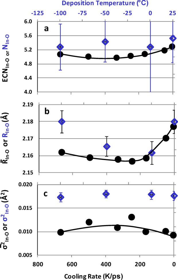
First-shell, In–O. (a) Effective coordination number, (b) average bond distance, and (c) bond-distance statistical spread obtained from the MD simulations for 80-atom cell a-InO with different cooling rates on bottom axis (black circle markers). Blue diamond markers, low deposition temperature region (top axis) of EXAFS data.
Figure 12.
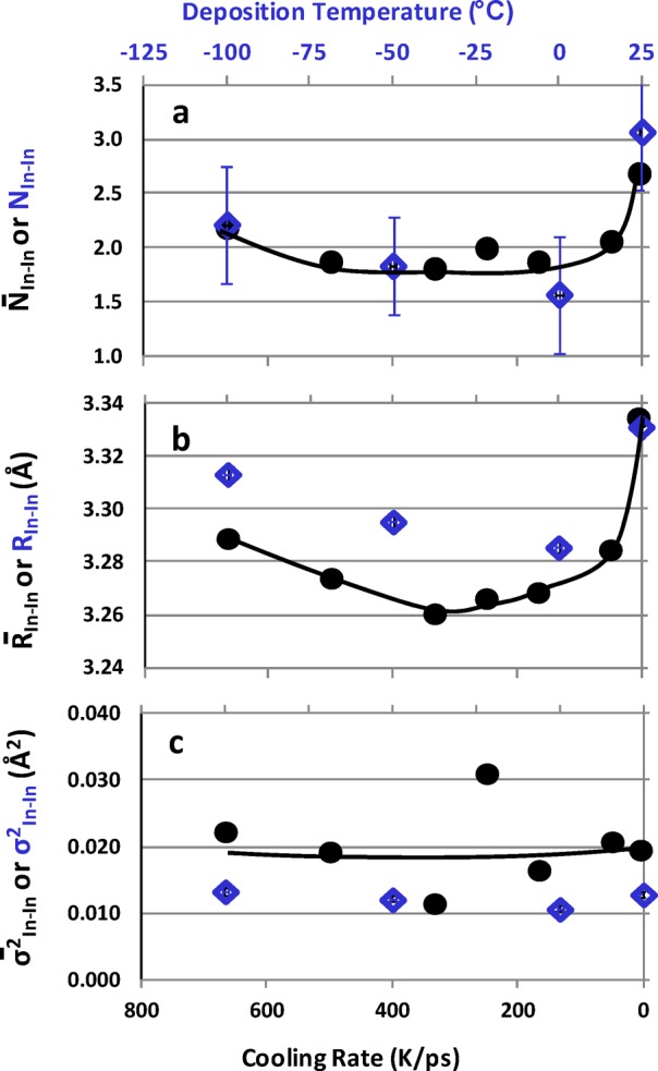
Second-shell, In–In. (a) Coordination number, (b) average bond distance, and (c) bond-distance statistical-spread obtained from the MD simulations for 80-atom cell a-IO with different cooling rates on the bottom axis (black circle markers). Blue diamond markers, low deposition temperature region (top axis) of EXAFS.
Figure 14.
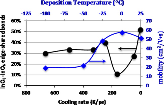
Percent contribution edge-shared InO6–InO6 polyhedra with respect to total (edge and corner) shared InO6 pairs as a function of cooling rate (black): Low temperature region of Hall mobility versus deposition temperature curve of Figure 5 (blue).
As already mentioned above, experimental description of the In–In distribution in amorphous oxides is challenging; theoretical works also lack important details about the In–In distances and coordination in amorphous oxides. The challenge arises from the proximity of the second and third shells (at 3.35 and 3.83 Å in c-IO), causing the corresponding pair distribution functions to overlap in the amorphous state. The total In–In distribution becomes over 1 Å wide, making the exponential fit in the ECN calculations inapplicable.
In order to distinguish between the second and third shells, the optimized atomic coordinates of the MD simulated structures were used to perform the following analysis. For every In atom, the number of In neighbors that share one, two, or three oxygen atoms with the central In atom was determined. The resulting average In–In coordination numbers represent corner, edge, or face-shared In–In, respectively. In this analysis, the maximum In–O distance to be considered as an In–O bond was set to 2.36 Å. This cutoff value is greater than the longest first-shell In–O distance in crystalline In2O3 and ensures that most of the first-shell In–O distances in the In–O pair distribution function (i.e., those that belong to the first-shell peak) are included. The In–In pair distribution functions calculated separately for edge-shared and corner-shared In atoms are given in Figure 11a. In addition, the average In–In distances, coordination numbers, and statistical spreads for both edge- and corner-shared In–In pairs were calculated, Figure 12. (The large statistical spread (Figure 12c) would certainly render the EXAFS data to contain little, if not be completely absent of, information on the third shell or corner-shared In–In interaction.) On the basis of the results, the following three important conclusions can be made:
Figure 11.
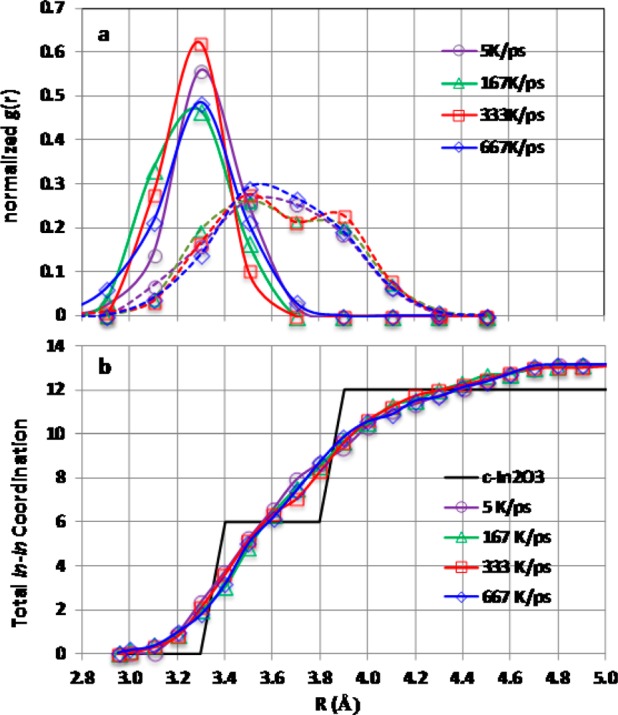
(a) Pair distribution functions for edge-shared In–In (solid lines: centered at ∼3.4 Å) and corner-shared In–In (dashed lines: centered at ∼3.7 Å) as obtained from the MD simulations for 80-atom cell a-IO with different cooling rates. (b) Total In–In coordination as a function of distance.
1. The edge-shared In–In distances are distributed between 3.0 and 3.8 Å with the peak located around 3.3 Å, Figure 11a, which corresponds to the second shell edge-shared In–In distance in c-IO. The average In–In distance calculated for the edge-shared In–In pairs, R̅In–In, varies with cooling rate, Figure 12b: the lowest values of 3.26–3.27 Å were obtained for the structures cooled at 333–167 K/ps. The trend in R̅In–In agrees well with the experimental observation for the second shell RIn–In, Figure 9b, where the lowest value of 3.28 Å was observed for the structure deposited at 0 °C. Furthermore, the calculated edge-shared In–In coordination, N̅In–In, remains at about 2.0 for all structures except for the one cooled at the slowest rate, in excellent agreement with the experiment, Figure 9a. The value of N̅In–In increases to 2.7 for the most “ordered” structure (5 K/ps) as might be expected toward the onset of crystallinity. Thus, the number of edge-shared In–In does not determine the transport properties in oxides.
2. Although the edge-shared In–In coordination is significantly suppressed (from 6 to 2) in a-IO, the total In–In coordination which combines face-, edge-, corner, and non-sharing In–In pairs, remains close to the one for the c-IO Figure 11b: the total In–In coordination reaches 6 at about 3.6 Å and 12 at about 4.2 Å in all amorphous IO structures independent of the cooling rates. Hence, a significant part (about 60%) of the edge-shared In–In pairs become corner-shared upon amorphization, as, indeed, can be seen from the average corner-shared In–In coordination of about 8, Figure 13, left axis.
Figure 13.
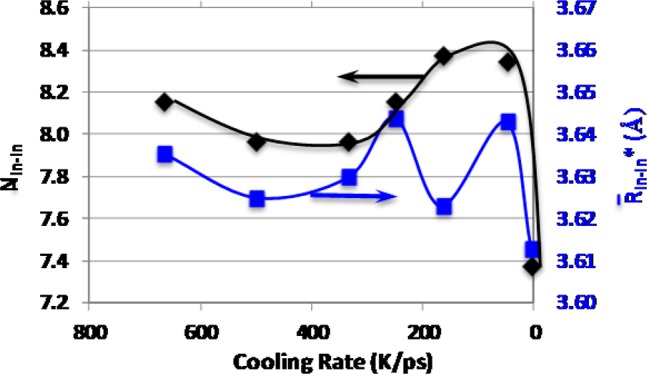
Third-shell, black diamonds: left axis, In–In* coordination number. Blue squares: right axis, average bond distance.
3. Accordingly, the corner-shared In–In distance distribution begins at around 3.0 Å, Figure 11a, resulting in a significant overlap with the edge-shared In–In distribution function. This finding highlights the challenge in distinguishing between the second and third shells from the general pair distribution function. Moreover, the corner-shared In–In distance distribution is almost twice as wide as the edge-shared one and includes long In–In distances at and above 4 Å. The average corner-shared In–In distance, R̅In–In*, is about 3.63 Å for all structures (Figure 13, right axis) which is smaller than the crystalline corner-shared In–In distance of 3.8 Å.
Because the In–O (first-shell) distances are generally preserved upon amorphization, c.f., Figures 6 and 10, the wide distribution of the corner-shared In–In distances determines the In–O–In angle distribution. The In–O–In angle defines the connection between the InOx polyhedra as well as the molecular p orbital of the oxygen atoms. To understand the role played by the In–O–In angle in the properties of amorphous oxides, the In–O–In angle distribution for corner- and edge-shared In–In pairs was calculated (given in the Supporting Information).
As expected, the edge-shared In–O–In angle distribution is narrow with the average value of 98° which is close to the edge-shared In–O–In angle value of 99.5° in c-IO. Also, the values of the average edge-shared In–O–In angle in a-IO vary insignificantly with the cooling rate. For the corner-shared In–In pairs, the average In–O–In angle is 115°, which does not have an analogous value in c-IO. The corner-shared In–O–In angle distribution function is wide, ranging from 95° to 130°, with two visible peaks at 109° and 124°. The latter angle value is close to the corner-shared In–O–In angle of 126° in c-IO. Importantly, the structures, obtained via intermediate cooling rates (333 K/ps and 250 K/ps), exhibit a plateau in the corner-shared In–O–In angle distribution having the weight of the first peak reduced, and a shoulder appears at 140°. Indeed, these structures exhibit the largest average In–O–In angle of 134° (calculated for corner-shared In–In distance range of 3.9–4.1 Å) as compared to 129–131° for both the fastest and slowest cooling rates.
Strikingly, the intermediate cooling rates resulted in the structures with the lowest distances, RIn–O (R̅In–O) and RIn–In (R̅In–In), and coordination numbers, NIn–O (N̅In–O) and NIn–In (R̅In–In), for the first and second shells as obtained both from the experiment and theoretical simulations. Since the structures with largest corner-shared In–O–In bond angle (obtained via intermediate cooling rates, 333 K/ps and 250 K/ps) seem to correspond to the highest mobility observed near the deposition temperature of 0 °C (Figure 4), it is critical to investigate this further. A large In–O–In angle may suggest a higher-symmetry molecular orbital for the oxygen p states, and, hence, a better overlap between the spherical s states of In atoms with the two directional p orbitals of the shared oxygen atom, giving rise to a smaller electron effective mass. However, the obtained angle deviations cannot result in a significant change in the effective mass; another mechanism should be responsible for the observed 3-fold mobility increase near the amorphous–crystalline transition. As mentioned above, the In–O–In angle determines the spatial distribution of the InOx polyhedral, i.e., the way the InOx polyhedra are connected. Large corner-shared In–O–In angles correspond to a longer In–In distances (of ∼4.0 Å on average); hence, one can suggest a formation of connected In–O–In chains in these structures. Spatially spread, connected chains may represent long conductivity paths and lead to an enhanced mobility.
To verify the above assumption, the atomic structures of the a-IO obtained via different cooling rates were analyzed. First, we identify the InO6 polyhedra in every structure and determine the number of the corner- and edge-shared pairs for the InO6 polyhedra only; Figure 14 is the percentage of edge-shared InO6–InO6 bonds as a function of cooling rate. We find that the slow-cooled structure (5 K/ps) possesses the largest number of edge-shared InO6–InO6 bonds (above 50%), whereas for fast-cooled structures (300 K/ps and above), the contribution from the edge-shared InO6 pairs remains at about 30%. Most strikingly, the number of edge-shared InO6 pairs is suppressed to as low as 10% for the structure obtained via 166 K/ps cooling rate so that the InO6 polyhedra are primarily connected via corner-sharing polyhedra. Also plotted on Figure 14 is the low temperature region of Figure 5, Hall mobility as a function of deposition temperature. The maximum in mobility coincides with the minimum in edge-shared InO6 pairs; the alignment of the deposition temperature and cooling rate scale is consistent with that used to compare the simulations with the EXAFS data.
In Figure 15, the spatial distributions of the InO6 polyhedra are plotted for the representative structures—those obtained via 500 K/ps, 250 K/ps, and 50K/ps quench rates. The following important observations are made. In the fast-cooled samples (500 K/ps and above), disconnected InO6 polyhedra and small clusters of 2–3 InO6 polyhedra connected via corner sharing were found. In contrast, the samples obtained via intermediate cooling rates (333–167 K/ps) feature long chains of mostly corner-shared InO6 polyhedra. As discussed above, these cooling rates correspond to an increased probability for large In–O–In angles and long In–In distances. Consequently, at these cooling rates the InO6 are connected throughout the cell, enabling continuing conductivity paths for charge carriers. At a slower cooling rate, the number of edge-shared In–In pairs increases, Figures 9a and 12a. Indeed, in the slow-cooled samples (50–5K/ps), large clusters of InO6 connected via edge and face sharing were found. Such clusters represent the on-set of nucleation of crystallites observed above the amorphous–crystalline transition (i.e., above the room temperature), Figure 4. The presence of such crystallites in the multiphase system leads to an enhanced scattering and, hence, to a decreased mobility. From additional MD simulations of a-IO within an 180-atom cell, the trends in the spatial distribution of InO6 polyhedra with the cooling rates were confirmed; moreover, it was found that at slow cooling rates (83 K/ps) the large InO6 clusters are disconnected from each other, even at an In–In distance as large as 4.0 Å.
Figure 15.
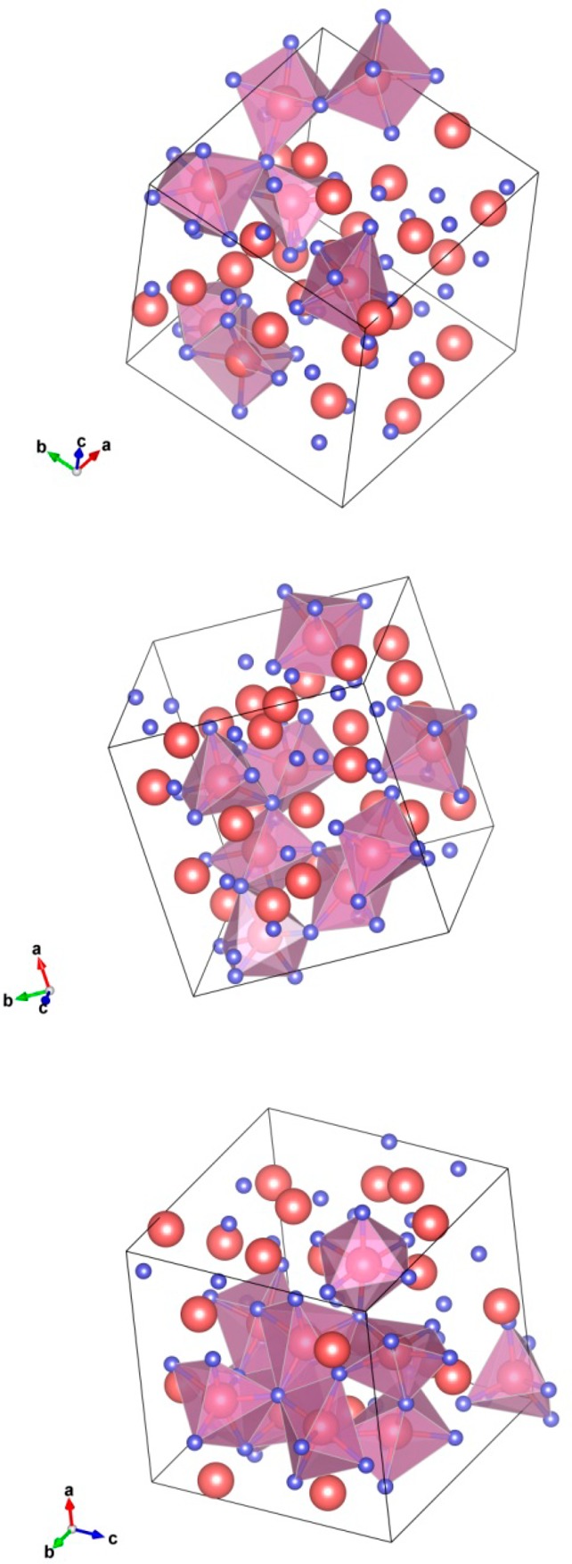
Spatial distribution and connectivity of the InO6 polyhedra in amorphous InO obtained via 500 K/ps (top), 250 K/ps (middle), and 50 K/ps (bottom) cooling rates. Indium and oxygen atoms are shown with large (red) and small (blue) balls. Only InO6 polyhedra are shown in these plots.
Conclusions
Thorough experimental and theoretical analyses of the structural characteristics of IO systems reveal the key mechanisms governing the properties of this oxide under amorphous-to-crystalline transition. The EXAFS and MD results for coordination numbers, bond distances, and statistical spreads are consistent with a concept of an amorphous oxide structure as one built of InOx polyhedra joined at the corners or edges to form a network structure in which the number of edge-sharing polyhedra are greatly diminished. Based on excellent agreement between EXAFS experimental results and MD liquid quench simulations obtained for the first and second shells of a-IO, important conclusions about the third shell (corner-shared In–In) were derived from the MD simulations.
The local maximum in Hall mobility observed at the onset of crystallinity has several plausible contributing factors. The minimum in the first shell (In–O) and the second shell (In–In) bond distances coincides with the maximum in mobility and can be a contributing factor to a small effective mass. Significant reduction of the edge-shared In–In coordination (from 6 to 2) is associated with a wide distribution of the corner-shared In–In distances and the corresponding In–O–In bond angles that determine the interconnection of the InOx polyhedra. Large In–O–In bond angles facilitate a higher symmetry p orbital on the shared oxygen atom leading to a better overlap with the s states of In atoms. A more significant factor that results from the increase in the In–O–In bond angle, however, is a transition from disconnected InOx clusters to extended connected chains of InOx polyhedra that can form long conductivity paths. The in-depth understanding of the structural characteristics opens up a route to attain optimal properties in technologically viable amorphous oxide semiconductors.
Acknowledgments
For this research, R.P.H.C., R.K., and J.E.M. were supported by the MRSEC program of the National Science Foundation at Northwestern University under grant no. DMR-1121262. D.B.B. was supported by the U.S. Department of Energy, Office of Science, Office of Basic Energy Sciences under the Award Number DE-FG02-06ER46320. This work made use of the J.B. Cohen X-ray Diffraction Facility supported by the MRSEC program of the National Science Foundation (DMR-1121262) at the Materials Research Center of Northwestern University; the Optical Microscopy and Metallography Facility MRSEC program of the National Science Foundation. X-ray absorption measurements were performed at the DuPont–Northwestern–Dow Collaborative Access Team (DND-CAT) located at Sector 5 of the Advanced Photon Source (APS). DND-CAT is supported by E.I. DuPont de Nemours & Co., The Dow Chemical Company, and Northwestern University. Use of the APS, an Office of Science User Facility operated for the U.S. Department of Energy (DOE) Office of Science by Argonne National Laboratory, was supported by the U.S. DOE under Contract No. DE-AC02-06CH11357. Computational resources were provided by the NSF-supported XSEDE program, grant TG-DMR080007. Electron microscopy was supported by the National Center for Research Resources (5 G12RR013646-12) and Department of Defense #64756-RT-REP. D.A., A.P., and M.J.-Y. also thank NSF PREM Grant # DMR 0934218.
Supporting Information Available
The EXAFS studies done on amorphous indium oxide base materials are reviewed, the rationale by which the parameters used in the EXAFS analysis were chosen and the problems encountered with the third shell analysis of the amorphous samples is presented, as well as the graphs of the In–O–In bond angle distribution of the edge and corner shared polyhedra obtained by the MD simulations. This material is available free of charge via the Internet at http://pubs.acs.org.
The authors declare no competing financial interest.
Funding Statement
National Institutes of Health, United States
Supplementary Material
References
- Freeman A. J.; Poppelmeier K. R.; Mason T. O.; Chang R. P. H.; Markd T. J. Film Stratagies for New Transparent Conducting Oxides. MRS Bull. 2000, 25, 45–51. [Google Scholar]
- Ginley D. S.; Bright C. Transparent Conducting Oxides. MRS Bull. 2000, 25, 15–18. [Google Scholar]
- Wagner J. F.; Keszler D. A.; Presley R. E.. Transparent Electronics; Springer: New York, 2008. [Google Scholar]
- Fortunato E.; Ginley D.; Hosono H.; Paine D. C. Transparent Conducting Oxides for Photovoltaics. MRS Bull. 2007, 32, 242–247. [Google Scholar]
- Hosono H. Ionic amorphous oxide semiconductors: Material design, carrier transport, and device application. J. Non-Cryst. Solids 2006, 352, 851–858. [Google Scholar]
- Ginley D. S.; Hosono H.; Paine D. C.. Handbook of Transparent Conductors; Springer: New York, 2010. [Google Scholar]
- Buchholz D. B.; Proffit D. E.; Wisser M. D.; Mason T. O.; Chang R. P. H. Electrical and band-gap properties of amorphous zinc-indium-tin oxide thin films. Prog. Nat. Sci.: Mater. Int. 2012, 1–6. [Google Scholar]
- Nomura K.; Ohta H.; Takagi A.; Kamiya T.; Hirano M.; Hosono H. Room-temperature fabrication of transparent flexible thin-film transistors using amorphous oxide semiconductors. Nature 2004, 432, 488–492. [DOI] [PubMed] [Google Scholar]
- Ito M.; Kon M.; Miyazaki C.; Ikeda N.; Ishizaki M.; Matsubara R.; Ugajin Y.; Sekine N. Amorphous oxide TFT and their applications in electrophoretic displays. Phys. Status Solidi A 2008, 205, 1885–1894. [Google Scholar]
- Chae G. S. A Modified Transparent Conducting Oxide for Flat Panel Displays Only. Jpn. J. Appl. Phys., Part 1 2001, 40, 1282–1286. [Google Scholar]
- Taylor M. P.; Readey D. W.; van Hest M. F. A. M.; Teplin C. W.; Alleman J. L.; Dabney M. S.; Gedvilas L. M.; Keyes B. M.; To B.; Perkins J. D.; Ginley D. S. The Remarkable Thermal Stability of Amorphous In-Zn-O Transparent Conductors. Adv. Funct. Mater. 2008, 18, 3169–3178. [Google Scholar]
- Kim W. M.; Ku D. Y.; Lee I.-k.; Seo Y. W.; Cheong B.-k.; Lee T. S.; Kim I.-h.; Lee K. S. The electromagnetic interference shielding effect of indium-zinc oxide/silver alloy multilayered thin films. Thin Solid Films 2005, 473, 315–320. [Google Scholar]
- Ryu M. K.; Yang S.; Park S.-H. K.; Hwang C.-S.; Jeong J. K. Appl. Phys. Lett. 2009, 95, 072104–1(3). [Google Scholar]
- Lee D. Y.; Lee J. R.; Lee G. H.; Song P. K. Study on In-Zn-Sn-O and In-Sn-Zn-O films deposited on PET substrate by magnetron co-sputtering system. Surf. Coat. Technol. 2008, 202, 5718–5723. [Google Scholar]
- Bellingham J. R.; Phillips W. A.; Adkins C. J. Electrical and optical properties of amorphous indium oxide. J. Phys.: Condens. Matter 1990, 2, 6207–6221. [Google Scholar]
- Harvey S. P.; Mason T. O.; Buchholz D. B.; Chang R. P. H. Carrier generation and inherent off-stoichiometry in Zn, Sn codoped indium oxide (ZITO) bulk and thin-film specimens. J. Am. Ceram. Soc. 2008, 91, 467–472. [Google Scholar]
- Buchholz D. B.; Liu J.; Marks T. J.; Zhang M.; Chang R. P. H. Control and Characterization of the Structural, Electrical, and Optical Properties of Amorphous Zinc-Indium-Tin Oxide Thin Films. ACS Appl. Mater. Interfaces 2009, 1, 2147–2153. [DOI] [PubMed] [Google Scholar]
- Kulkarnia A. K.; Schulzb K. H.; Lima T. S.; Khanb M. Dependence of the sheet resistance of indium-tin-oxide thin films on grain size and grain orientation determined from X-ray diffraction techniques. Thin Solid Films 1999, 345, 273–277. [Google Scholar]
- Tahar R. B. H.; Ban T.; Ohya Y.; Takahashi Y. Tin doped indium oxide thin films: Electrical properties. J. Appl. Phys. 1998, 83, 2631–2645. [Google Scholar]
- Rehr J. J.; Albers R. C. Theoretical approaches to x-ray absorption fine structure. Rev. Mod. Phys. 2000, 723621–654. [Google Scholar]
- Stern E. A.; Sayers D. E.; Lytle F. W. Extended x-ray-absorption fine-structure technique. III. Determination of physical parameters. Phys. Rev. B 1975, 11124836–4846. [Google Scholar]
- Nomura K.; Kamiya T.; Ohta H.; Uruga T.; Hirano M.; Hosono H. Local coordination structure and electronic structure of the large electron mobility amorphous oxide semiconductor In-Ga-Zn-O: Experiment and ab initio calculations. Phys. Rev. B 2007, 75, 035212. [Google Scholar]
- Aliano A.; Catellani A.; Cicero G. Characterization of amorphous In2O3: An ab initio molecular dynamics study. Appl. Phys. Lett. 2011, 99, 211913. [Google Scholar]
- Ramzan M.; Kaewmaraya T.; Ahuja R. Molecular dynamics study of amorphous Ga-doped In2O3: A promising materials for phase change memory devices. Appl. Phys. Lett. 2013, 103, 072113. [Google Scholar]
- Rosen J.; Warschkow O. Electronic structure of amorphous indium oxide transparent conductors. Phys. Rev. B 2009, 80, 115215. [Google Scholar]
- Walsh A.; Da Silva J. L. F.; Wei S.-H. Interplay between Order and Disorder in the High Performance of Amorphous Transparent Conducting Oxides. Chem. Mater. 2009, 21, 5119–5124. [Google Scholar]
- Davis S.; Gutierrez G. Structural, elastic, vibrational and electronic properties of amorphous Al2O3 from ab-initio calculations. J. Phys. Cond. Matter 2011, 23, 495401. [DOI] [PubMed] [Google Scholar]
- Kim M.; Kang I. J.; Park C. H. First-principle study of electronic structure of Sn-doped amorphous In2O3 and the role of O-deficiency. Curr. Appl. Phys. 2012, 12, S25–S28. [Google Scholar]
- Nishio K.; Miyazaki T.; Nakamura H. Universal Medium-Range Order of Amorphous Metal Oxides. Phys. Rev. Lett. 2013, 111, 155502. [DOI] [PubMed] [Google Scholar]
- Deng H.-X.; Wei S.-H.; Li S.-S.; Li J.; Walsh A. Electronic origin of the conductivity imbalance between covalent and ionic amorphous semiconductors. Phys. Rev. B 2013, 87, 125203. [Google Scholar]
- Ravel B.; Newville M. ATHENA, ARTEMIS, HEPHAESTUS: Data analysis for X-ray absorption spectroscopy using IFEFFIT. J. Synchrotron Radiat. 2005, 12, 537–541. [DOI] [PubMed] [Google Scholar]
- Kresse G.; Hafner J. Ab initio molecular-dynamics for liquid-metals. Phys. Rev. B 1993, 47, 558–561. [DOI] [PubMed] [Google Scholar]
- Kresse G.; Hafner J. Ab initio molecular-dynamics simulation of the liquid-metal-amorphous-semiconductor transition in germanium. Phys. Rev. B 1994, 49, 14251–14269. [DOI] [PubMed] [Google Scholar]
- Kresse G.; Furthmuller J. Efficiency of ab initio total energy calculations for metals and semiconductors using plane-wave basis set. Comput. Mater. Sci. 1996, 6, 15–50. [Google Scholar]
- Kresse G.; Furthmuller J. Efficient iterative schemes for ab initio total-energy calculations using a plane-wave basis set. Phys. Rev. B 1996, 54, 11169–11186. [DOI] [PubMed] [Google Scholar]
- Perdew J. P.; Burke K.; Ernzerhof M. Generalized Gradient Approximation Made Simple. Phys. Rev. Lett. 1996, 77, 3865–3868. [DOI] [PubMed] [Google Scholar]
- Stich I.; Car R.; Parrinello M. Amorphous silicon studied by ab initio molecular dynamics: Preparation, structure, and properties. Phys. Rev. B 1991, 44, 11092–11104. [DOI] [PubMed] [Google Scholar]
- Noh H.; Chang K. J. Electronic structure of oxygen-vacancy defect in amorphous In-Ga-Zn-O semiconductors. Phys. Rev. B 2011, 84, 115205. [Google Scholar]
- Marks N. A. Evidence for subpicosecond thermal spikes in the formation of tetrahedral amorphous carbon. Phys. Rev. B 1997, 56, 5. [Google Scholar]
- Yoshida T.; Tanabe T.; Yoshida H. XAFS Study of Silica Glasses Irradiated by High-Energy Particles. Phys. Scr. 2005, T115, 435–438. [Google Scholar]
- Buchholz D. B.; Zeng L.; Bedzyk M. J.; Chang R. P. H. Differences Between Amorphous Indium Oxide Thin Films. Prog. Nat. Sci.: Mater. Int. 2013, 23, 475–480. [Google Scholar]
- Hoppe R. The Coordination Number – an Inorganic Chameleon. Angew. Chem., Int. Ed. Engl. 1970, 9, 25–34. [Google Scholar]
- Hoppe R.; Voigt S.; Glaum H.; Kissel J.; Muller H. P.; Bernet K. A New Route to Charge Distribution in Ionic Solids. J. Less-Common Met. 1989, 156, 105–122. [Google Scholar]
Associated Data
This section collects any data citations, data availability statements, or supplementary materials included in this article.


