Abstract

We present metallic nanohole arrays fabricated on suspended membranes as an optofluidic substrate. Millimeter-sized suspended nanohole arrays were fabricated using nanoimprint lithography. We demonstrate refractive-index-based tuning of the optical spectra using a sucrose solution for the optimization of SERS signal intensity, leading to a Raman enhancement factor of 107. Furthermore, compared to dead-ended nanohole arrays, suspended nanohole arrays capable of flow-through detection increased the measured SERS signal intensity by 50 times. For directed transport of analytes, we present a novel methodology utilizing surface tension to generate spontaneous flow through the nanoholes with flow rates of 1 μL/min, obviating the need for external pumps or microfluidic interconnects. Using this method for SERS, we obtained a 50 times higher signal as compared to diffusion-limited transport and could detect 100 pM 4-mercaptopyridine. The suspended nanohole substrates presented herein possess a uniform and reproducible geometry and show the potential for improved analyte transport and SERS detection.
Introduction
The emerging field of optofluidics explores new possibilities to combine optical detection techniques with micro- and nanofluidics1−3 to develop miniaturized optical sensors with improved performance. The analytical techniques commonly used include surface plasmon resonance (SPR), surface-enhanced Raman spectroscopy (SERS), and fluorescence imaging.4 SERS, a powerful technique for biosensing and chemical identification, largely depends on the drastic enhancement of weak Raman signal obtained from analyte molecules, upon their interaction with optical near-fields of metallic nanostructures.5,6 As an analytical technique, SERS combines the benefits of label-free sensing, high sensitivity, and chemical specificity. An important aim is to further improve the capabilities of SERS for diverse applications such as healthcare and environmental monitoring using substrates that can be fabricated reproducibly and have a uniform geometry.7 As the enhancement of electromagnetic fields occurs in nanoscale regions, termed as plasmonic hotspots, integration of microfluidics capable of directing the analyte flow and resultant concentration toward these hotspots can improve the sensitivity and reduce the detection time for SERS.8−11 Among various options, we explore metallic nanohole arrays fabricated in suspended silicon nitride (Si3N4) membranes because they provide a unique option to integrate SERS with flow-through sensing, which has yet to be shown experimentally.
Nanohole arrays in thin metallic films can act as plasmonic substrates with multifarious applications. Enhancement of the electromagnetic field and extraordinary optical transmission (EOT) through the nanoholes has led to their application in plasmonic sensing.12−15 Primarily, they have been used as a platform for SPR refractive-index sensing.16−20 While groups have demonstrated nanohole-enhanced Raman spectroscopy,21−24 the reported Raman enhancement factors (below ∼105) are weaker than that of other SERS substrates. These previous experiments relied on low-throughput fabrication techniques such as focused ion beam (FIB) or electron-beam lithography to pattern nanoholes in a metal film. Suspended nanohole arrays have been utilized for SPR sensing, but have not been utilized for SERS. Flow-through suspended nanoholes have been utilized for overcoming diffusion-limited transport in SPR sensing.10,11,25−27 Most of these methods, however, require external sources for generating pressure gradients, which can often damage the fragile membrane, and microfluidic tubing or an external power supply for creating an electric field. A simple and robust sample delivery mechanism is needed for flow-through sensing.
In this work, nanoimprint lithography (NIL)28−31 is used to fabricate periodic Ag nanohole arrays over a millimeter-sized suspended silicon nitride (Si3N4) membrane with high throughput and reproducibility. To improve the Raman enhancement factor (EF) on these large-area substrates, plasmon resonances of suspended nanohole arrays are precisely tuned using a sucrose solution. We report a high Raman EF of up to 107 for silver-coated suspended nanoholes using this technique. Furthermore, suspended nanohole arrays are capable of fast flow through the nanoholes driven by surface tension forces, which promote adsorption of the analytes toward the plasmonic hotspot and further boost the SERS signal by 50 times compared to diffusion-limited transport. Using this optofluidic SERS substrate, we detect a 100 pM 4-mercaptopyridine (4-MP) sample.
Experimental Methods
Fabrication of Large-Area Suspended Nanohole Arrays
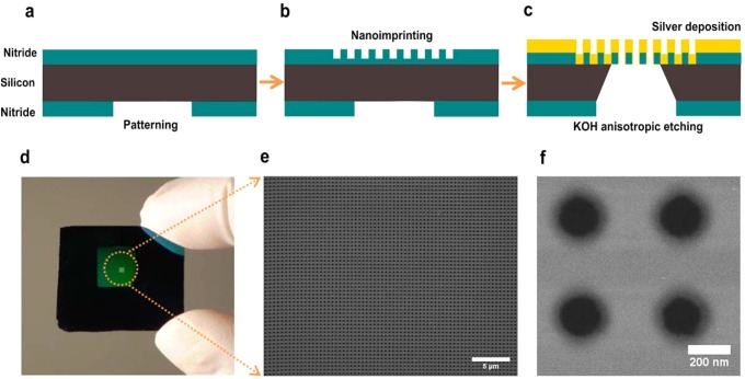
Suspended nanohole arrays were fabricated over a region of 1 mm2 in size using nanoimprint lithography (NIL), as shown in Figure 1a–c. Low-stress silicon nitride (200 nm) was deposited on both sides of single-sided polished (100) silicon wafers using low-pressure chemical vapor deposition (LPCVD). These wafers were then patterned using photolithography and dry etching such that some regions on the back of the wafers had nitride removed, exposing the silicon. Nanoimprint resist was then spun over the top surface of the wafer. A nanoimprint mold was carefully placed on the resist so that it aligned well with patterns etched on the back of the wafer. The mold used for nanoimprinting had pillars with a 200 nm diameter, 500 nm periodicity, and 300 nm pillar height over a 1 cm × 1 cm area. Nanoimprinting generated nanohole patterns in the resist layer. The sample was further processed to etch the nanohole arrays into the top nitride layer. The etching was done for a fixed time period such that the holes go about two-thirds of the way into the nitride. This was necessary to protect the silicon from subsequent KOH etching. The nanoimprint resist was then cleaned off, and samples were placed in a KOH bath for anisotropic etching. A suspended nitride membrane with nanohole array patterns was obtained. The samples were further dry-etched to remove the remaining nitride from the bottom of the nanoholes and obtain suspended open-ended nanoholes. Silver (120 nm) was then deposited on the top of the samples using an electron-beam evaporator.
Figure 1.
Fabrication of suspended nanohole array chip. (a) A silicon chip after 200 nm low-stress nitride deposition and photolithography to expose desired regions on the backside. (b) Nanoimprinting and dry etching was performed to transfer the nanohole array pattern to the top nitride membrane. Nanoimprint resist was then washed away. (c) Anisotropic KOH etching of silicon was used to obtain the suspended nitride membrane. A final dry etch removed the remaining nitride from the bottom of the holes. Silver was then evaporated from the top to obtain suspended metallic nanohole arrays. (d) A 1 in. × 1 in. chip with a 1 cm × 1 cm nanoimprinted region in the center. The nanoimprinted region further has a 1 mm × 1 mm suspended membrane in the center (circled). (e) SEM image of the suspended membrane with nanoholes. (f) SEM shows magnified image of the individual nitride nanoholes.
Raman Spectroscopy
For Raman measurements of benzenethiol (BZT) and 4-MP solutions, a quartz cuvette with a 1 mm path length was used. A 785 nm diode laser with an incident power of 10 mW was loosely focused onto the sample using a 10× objective. The Raman scattered light was collected in transmission mode using a 50× objective (NA 0.5) and passed onto a spectrometer (Ocean Optics QE65000) through a multimode fiber after removing the excitation light with a notch filter. The acquisition time was 30 s. Neat BZT (∼10 M) and 0.6 M 4-MP solution were used to acquire the Raman spectra. For formation of a self-assembled monolayer (SAM), chips were placed in 1 mM BZT (eth.) or 1 mM 4-MP (aq.) overnight. They were then rinsed thrice with ethanol (BZT samples) or deionized (DI) water (4-MP samples) over a period of 30 min. The parameters used for calculation of the enhancement factor are described in the Supporting Information.
Optical Analysis
The chips were placed on a Nikon Eclipse LV 100 upright microscope stage with a 10× objective, and a fiber-optic spectrometer was used to record transmission spectra through the nanoholes. Sucrose solutions of desired concentrations (0–1.5 M) were used to tune the transmission spectra. The SERS signal was then obtained from the samples. ImageJ software was used for analysis and coloring of the images. Data plots were prepared using Matlab (MathWorks, Inc.) and GraphPad Prism version 5.04 (GraphPad Software, Inc.).
Computational Modeling
Three-dimensional (3D) finite-difference time-domain (FDTD) simulations around the suspended nanoholes were performed using FullWAVE simulation software. (RSoft, Inc.) A single hole was simulated with periodic boundary conditions on the faces intersected by the metal film to represent an infinite hole array and absorbing boundary conditions on the final two faces. A grid size of 3 nm was used around the hole in all dimensions. The index of refraction for the nitride was set at 2, the optical constants for silver were measured via ellipsometry, and the refractive indices of materials surrounding the hole array were varied. The excitation wavelength was set to 785 nm to match experiments.
Surface-Tension-Induced Flow
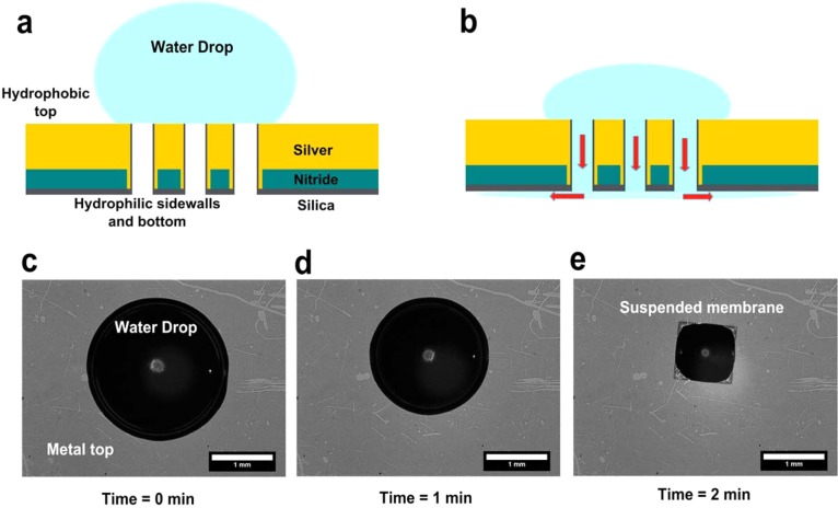
A 30 nm thick SiO2 film was deposited on the back of the samples using an electron-beam evaporator. Using this directional deposition technique, the sidewalls of the nanoholes, which lie parallel to the direction of evaporation, were coated with a much thinner layer of silica. The desired volume of aqueous solution was then added to the top surface of the chips, as shown in Figure 4.
Figure 4.
Schematic for surface-tension-induced flow through nanoholes. (a) Aqueous solution is placed over the nanoholes. The top metal surface is hydrophobic, whereas the silica layer within the holes and on the backside of the chip is hydrophilic. (b) Hydrophilic nanohole sidewalls suck in the solution, driving the flow toward the back of the chip (shown as red arrows). (c–e) Bright-field images showing flow of a 2 μL drop of water through the suspended nanohole array within 2 min. The water drop shrinks as it is sucked in through the hydrophilic nanohole sidewalls.
Bead and 4-MP Concentration
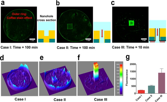
Fluorescent polystyrene beads were obtained from Bangs Laboratories (poly(Styrene/2%DiVinylBenzene/Vinyl-COOH), mean diameter: 2.19 μm) and were used at a final concentration of 106 beads/mL in DI water. A 10 μL solution containing beads was added on the top of the chips for the three cases I, II, and III, as shown in Figure 5. The samples were left undisturbed until the solution was consumed through evaporation or flow. The top was then imaged using a fluorescence microscope to monitor accumulation of particles. For SERS measurements, a 4-MP solution of desired concentration and volume was added to the top of the chips and allowed to completely flow through. Sucrose solution was used to obtain the optimized SERS signal from the chips, as discussed earlier. In the case of loss in the volume of sucrose from the top of the chip due to flow-through, fresh sucrose solution was added to the sensing region.
Figure 5.
Bead concentration and time taken for consumption of solution over nanohole arrays for three cases. (a) Case I: Accumulation of 2 μm polystyrene beads after evaporation of a 10 μL drop over dead-ended nanohole arrays. The schematic shows cross section of a single dead-ended nanohole for this case. (b) Case II: The same experiment performed over suspended nanohole arrays with metal-coated (hydrophobic) sidewalls. Evaporation from open end of nanoholes promotes directed flow and concentration. (c) Case III: These samples had silica deposited on the back surface and sidewalls, resulting in surface-tension-directed flow. (d–f) Surface plots corresponding to (a–c) representing the intensity of fluorescence over the suspended membrane. (g) Average fluorescence intensity calculated from beads accumulated over the suspended membranes after 3 rounds of experiments. These results demonstrate that Case III surface-tension-induced flow-through promotes the most effective concentration of particles over the nanoholes and is an order of magnitude faster than purely evaporation-driven concentration.
Results and Discussion
Suspended metallic nanohole arrays were fabricated on low-stress silicon nitride (Si3N4) membranes using NIL (Figure 1a–c). One such chip with a 1 cm × 1 cm area of imprinted nanohole arrays is shown in Figure 1d. The suspended membrane region, approximately 1 mm × 1 mm defined by KOH wet etching of Si, consisting of open-ended nanoholes is also indicated. A scanning electron micrograph (SEM) shows uniform suspended nanohole arrays (Figure 1e). An SEM image at higher magnification shows individual nanoholes in the silicon nitride membrane (Figure 1f). The holes are approximately 200 nm in diameter, and the array has a periodicity of 500 nm. Silver (thickness 120 nm) was deposited over the chips using electron-beam evaporation.
Optimization of SERS signal requires tuning of the plasmon resonances of the metallic substrate such that, for a given laser wavelength, there is maximum enhancement of electromagnetic field around nanoholes. Generally, modification of the design of the plasmonic substrate such as changing the periodicity of nanohole arrays or altering the wavelength of the laser source is used for this tuning.21,22,32 Here, we present a simple method to achieve desired plasmon resonance conditions on suspended nanohole arrays using refractive-index-based tuning. It has been established that surface-plasmon-mediated transmission can be modulated by the refractive index at the metal–dielectric interface. In fact, the shift in transmission peaks of nanohole arrays due to change in refractive index close to the sensor surface has been used for biosensing.16−19 We utilized this intrinsic property of metallic nanohole arrays to tune the resonance peaks. Here, we used sucrose solutions of appropriate concentration on the nanohole array surface to shift the transmission spectra as desired and tested the evolution of the SERS signal. Sugars like glucose and sucrose have been reported to be very difficult to detect using SERS owing to their small normal cross section and negligible adsorption to bare metal surfaces.33 This property makes them suitable to be used on a SERS substrate without adding unwanted Raman peaks.
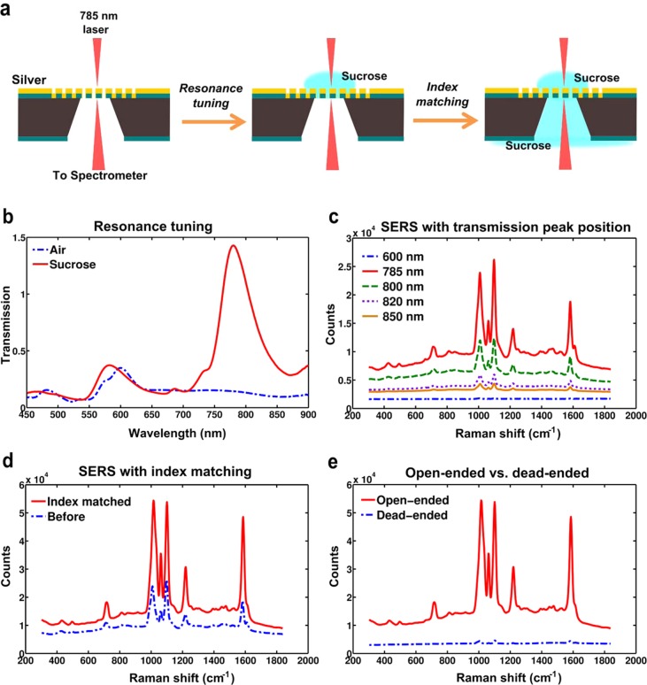
The schematic for SERS measurement and the steps for signal optimization from the suspended nanohole array chips are illustrated in Figure 2a. BZT and 4-MP were used to characterize the SERS response of the chips as these molecules are known to have large scattering cross sections and can easily form self-assembled monolayers (SAMs) owing to thiol–metal bonding on gold or silver. Chips with 4-MP SAM layers were used for the results shown in Figure 2. By increasing the concentration of the added sucrose solution, the transmission peak can be shifted to longer wavelengths. Upon addition of approximately 1 M sucrose solution, the transmission peak at 600 nm corresponding to the (1,0) silver–air interface was shifted to 785 nm (Figure 2b).
Figure 2.
Optimized SERS from suspended nanohole arrays. (a) Schematics showing the process of obtaining a SERS signal from chips with air as dielectric media, resonance tuning using sucrose to improve the signal, and index matching to further optimize the signal. (b) Figure showing normalized transmission maxima at around 600 nm corresponding to (1,0) metal–air interface shifts to 785 nm after addition of the desired concentration of sucrose. (c) SERS signal obtained from the same spot on the chip with the transmission peak tuned to different wavelengths. (d) SERS signal obtained from the same spot before and after index matching. There is close to 3 times increase in signal after index matching. (e) SERS signal obtained from 4-MP SAM layers on suspended nanohole arrays as compared to FIB milled dead-ended nanoholes. The signal from suspended nanoholes is about 50 times higher than that obtained from dead-ended samples.
SERS spectra were obtained from the sample with variation in the position of the transmission peak of the nanoholes (Figure 2c). These measurements were taken from the same spot on the sample to avoid any other sources of variation in signal. As expected, the maximum SERS signal was obtained when the peak transmission wavelength of the nanoholes matched the laser wavelength at 785 nm. Upon adding the same sucrose solution to the backside cavity of the suspended nanohole array membrane, a further increase (up to 300%) in the SERS signal was observed (Figure 2d). It has been known that surface-plasmon-enhanced transmission through nanoholes can be enhanced up to an order of magnitude by matching the refractive index on either side of the metal film.34
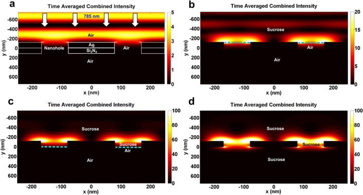
Three-dimensional (3D) finite-difference time-domain (FDTD) simulations were performed to demonstrate the increase in the plasmonic field around the nanohole arrays with refractive-index-based tuning (Figure 3). In the first case, air was used as the refractive index medium and weak plasmonic hotspots can be observed at the edges of the nanoholes (Figure 3a). With the addition of sucrose and filling of the nanoholes such that the transmission maxima is in resonance with the excitation wavelength (785 nm), more than an order of magnitude enhancement of the plasmonic field at the hotspots can be observed (Figure 3b,c). A further increase in electric field was obtained with sucrose present on both sides of the sample as well as inside the nanoholes (Figure 3d). The increase in electric field observed in these FDTD simulations correlates qualitatively with the measured increase in SERS signal (Figure 2c,d). For further comparison, samples with dead-ended hole arrays were prepared using FIB milling; 120 nm thick silver was deposited on suspended nitride membranes and nanoholes with diameter 200 nm and periodicity 500 nm were milled through the silver but not through the nitride membrane. These samples were also placed in a solution of 4-MP overnight to form a SAM layer. To measure the SERS signal from the dead-ended hole array samples, a drop of sucrose solution was added to the substrate such that the transmission peak matches the laser wavelength. The SERS signal obtained from an FIB milled dead-ended hole array sample as compared to the signal obtained from the suspended nanohole array under optimized transmission conditions is shown in Figure 2e. The signal obtained from suspended nanoholes was approximately 50 times higher as compared to dead-ended samples (Figure 2e). This difference could be attributed to a combination of a number of factors, including refractive index matching between the top and bottom sides of the suspended nanoholes, improved transmission, and nanoscale variations in geometry of the nanohole edges (hotspots) obtained via nanoimprinting as compared to ion milling.
Figure 3.
Three-dimensional FDTD simulations for suspended nanohole arrays with an excitation wavelength of 785 nm. Electric field intensity with (a) air as the dielectric medium around and inside the suspended nanoholes. (b) Sucrose present on the top metal surface. Air present inside and at the bottom end of the nanoholes. (c) Sucrose present on the top silver surface and filling top half of the nanoholes, whereas air is present elsewhere. Concentration of sucrose is adjusted such that the transmission maxima through the nanoholes matches the excitation wavelength (785 nm). (d) Sucrose present on both sides and completely filling the nanoholes.
Raman signals obtained from neat solutions of 4-MP and BZT were used to calculate enhancement factors for the chips. The vibration bands used for this calculation correspond to the in-plane ring breathing mode coupled to the C–S stretching for the BZT and 4-MP samples.35 When BZT adsorbed to the silver surface, the vibration band was observed to shift from 1092 to 1072 cm–1. Similarly for 4-MP, the vibration band shifted from 1115 cm–1 in aqueous solution to 1099 cm–1 upon adsorbing to the silver surface. Enhancement factors of ∼107 were obtained for the suspended nanoholes for both 4-MP and benzenethiol samples. These numbers were obtained repeatedly over multiple spots on different samples using both BZT and 4-MP as analytes. In comparison, previous studies on nanohole array SERS21,22,24 have reported EFs in the range of 104–105. This improvement in the EF values (∼100 times) obtained by our system confirms that suspended nanohole arrays can be used as excellent SERS substrates.
Nanohole-based biosensors with integrated flow-through fluidics can provide one route to overcome diffusion-limited transport of analytes, improving the detection time and detection limit of the sensor.10,11 To facilitate the flow-through process, silica (30 nm), which is hydrophilic, was deposited on the backside of the chips using electron-beam evaporation. As this deposition technique is highly directional, the sidewalls of the nanoholes, which lie parallel to the direction of evaporation, were coated with a much thinner layer of silica. The addition of the silica layer on the opposite side of sample injection drastically altered the flow properties of the chip. Figure 4 shows the schematic of chips with silica on the backside, and a hydrophobic top surface. When an aqueous solution of analyte or particles was placed on the top of the chip, flow through the nanoholes was initiated as soon as the solution came into contact with the hydrophilic inner walls. The solution then flowed and spread on the back surface of the chip. Figure 4c–e shows snapshots of the flow in process, where a 2 μL drop of water disappears through the nanohole membrane within 2 min. For membranes of size 1 mm2, we obtained an approximate flow rate of 1 μL/min.
The effect of flow-through concentration as compared to diffusion-limited adsorption or evaporation-driven concentration over suspended nanoholes was visualized using fluorescent 2 μm polystyrene beads. In Figure 5, we compare the accumulation of polystyrene beads (106 beads/mL) in three cases: (I) where the holes were dead-ended; (II) where the holes were open and concentration was driven by evaporation through the open-end of the nanoholes; and (III) holes were open and silica was deposited on the backside, leading to flow and concentration. Schematics for the cross section of a single nanohole accompany the fluorescence images for each of the three cases in Figure 5(a–c). During the evaporation of a liquid drop on a surface, evaporation of solution from the pinned outer edges generates an outward flow and concentrates particles at the edges. This phenomenon, known as the “coffee stain effect”,36 is clearly visible in images (a) and (b) in Figure 5. The particles were randomly distributed within the area of the drop, as shown in Figure 5a, as their position was determined by diffusion and the outer flow. In case II, open-ended holes with no silica also promoted evaporation-based localized flow and accumulation of particles over the nanohole array was obtained. There was no significant difference in the time scales of evaporation for cases I and II. For case III (open-ended holes with silica), the flow was based on surface tension and the time scale was an order of magnitude less than evaporation-based methods. This case demonstrates a significantly higher concentration as most of the solution was directed to flow through the nanoholes, improving particle aggregation over the holes (Figure 5c). The absence of a prominent outer ring for the drop indicates the dominance of nanohole directed flow and the relatively shorter time scale of the process. Surface plots revealing the intensity of fluorescence for these three cases are shown in Figure 5(d–f). The average fluorescence from the accumulated beads over the suspended membrane area was calculated over three rounds of experiments and is shown in Figure 5g.
These results illustrate that surface-tension-induced flow through nanoholes promotes the most efficient concentration of particles and is at least an order of magnitude faster as compared to evaporation-based techniques. This principle can also be utilized for overcoming diffusion-limited interaction of analytes with the nanoholes for plasmonic sensing. For small analyte molecules, the passive flow generated by surface tension forces drives them to pass within less than 100 nm (radius of the nanoholes) of the hotspot, i.e., edge of the nanoholes and the nanohole sidewalls. This short distance can be easily overcome by diffusion of analyte molecules increasing the probability of the analytes adsorbing on or close to the plasmonic hotspots, which can lead to enhancement of the Raman signal of analytes. The 4-MP molecules, which have a thiol group, can be captured on the nanohole array substrate through formation of covalent thiol–silver bonds. The molecules may also get physically adsorbed to silica layered regions inside the nanoholes through van der Waals forces.
To demonstrate the advantage of flow through the nanoholes over diffusion-based transport for SERS sensing, we performed experiments where the nanohole substrates were prepared in two different ways. In the first case, 20 μL of 100 nM 4-MP solution was allowed to completely flow through suspended nanoholes in about 20 min. For diffusion-based adsorption, substrates were submerged in a reservoir containing identical 4-MP solution for the same amount of time. The SERS signal obtained from both the samples is shown in Figure 6a. Samples with surface-tension-induced flow gave about 50 times higher signal as compared to diffusion-limited adsorption. The experiment was repeated over multiple sets of samples and similar results were observed (Figure S3, Supporting Information). To demonstrate detection of low concentration samples, 50 μL of 4-MP at a concentration of 100 pM (i.e., 5 fmol of 4-MP) was allowed to flow through the sample for about an hour. The SERS signal collected from this sample shown in Figure 6b demonstrates the capability of the method to detect low concentrations of analyte molecules. The high sensitivity in this case results from the combination of two factors: large Raman enhancement factor of the nanohole array substrate and flow-through-based concentration of molecules at the hot spot.
Figure 6.
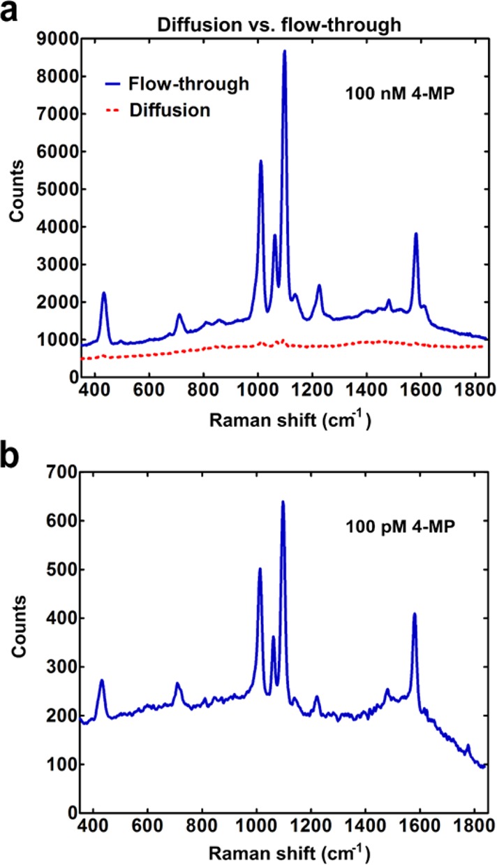
SERS with surface-tension-induced flow-through. (a) Comparison of SERS spectra obtained from flow-through of 100 nM 4-MP (red spectrum) as compared to diffusive transport (blue). (b) SERS spectra obtained after flow-through of 100 pM 4-MP for an hour.
The limit of detection of the setup, in terms of 4-MP concentration, would depend on the duration of time the solution is allowed to flow through the nanoholes. However, it can be estimated in terms of number of molecules of 4-MP in solution. Using the peak at 1099 cm–1 in the SERS signal shown in Figure 6b, the signal-to-noise (S/N) ratio was calculated to be approximately 55. Assuming a linear concentration vs signal response (Figure S2, Supporting Information), and calculating for a final S/N ratio of 3, gave us a limit of detection of approximately 272 amol of 4-MP molecules in solution.
Conclusion
We have demonstrated the fabrication of millimeter-sized suspended metallic nanohole arrays using NIL and their potential for flow-through SERS. Refractive-index-based tuning with sucrose solution was implemented on this suspended nanohole array substrate for optimized SERS. This tuning method was utilized to match the plasmon resonance peaks with the excitation laser wavelength. Sucrose solution was used because it has a very weak intrinsic Raman signal and, therefore, does not contribute detectable background to the measurements. This simple tuning method can also be utilized for plasmon-enhanced fluorescence37,38 where the plasmon resonance can be tuned based on the excitation or emission spectra of the fluorescent species. Furthermore, this technique can easily be translated to other plasmonic substrates utilizing the principle that, by changing the refractive index of the dielectric medium around the metal, plasmon resonance conditions can be changed to optimize the detection of the optical signal from analyte molecules. The suspended Ag nanohole arrays have a SERS enhancement factor on the order of 107, which is 2 orders of magnitude greater than those reported previously for nanohole arrays and compares well with other commonly used SERS substrates. Our demonstration of high SERS enhancement factor from nanohole arrays can open up many possibilities, because the nanohole geometry enables trapping of biomolecules and small particles,11,39 formation of model membranes such as suspended lipid bilayers,19,40−42 as well as flow-through sensing to overcome the diffusion limit.10,11,24−26 To combine nanohole-enhanced SERS with flow-through sensing, we have demonstrated surface-tension-induced passive flow and concentration of particles over the nanohole arrays. Passive flow rates of around 1 μL/min were obtained using this technique. This passive flow allowed us to overcome diffusion-limited transport of analytes and reduced the time required to consume the solution while bringing the analyte molecules closer to the plasmonic hotspots. Our device design utilizing passive flow obviates the use of a bulky external pump and fluidic interconnects, thus improving the simplicity and portability of the process. Thus, the simple and novel resonance tuning as well as passive flow-through technique discussed here on a suspended nanohole array platform can help alleviate the mass transport limitations and benefit wide applications in optofluidics.
Acknowledgments
This work was supported by grants from the National Science Foundation (NSF CAREER Award and DBI 0964216), the National Institutes of Health (NIH R01 GM 092993), and the Minnesota Partnership for Biotechnology and Medical Genomics. This work utilized resources at the University of Minnesota, including the Nanofabrication Center, which receives partial support from the NSF through the National Nanotechnology Infrastructure Network program, and the Characterization Facility, which has received capital equipment funding from the NSF through the Materials Research Science and Engineering Center. S.K. and T.W.J. acknowledge support from the University of Minnesota Doctoral Dissertation Fellowship. T.W.J. also acknowledges support from the NIH Biotechnology training grant.
Supporting Information Available
Parameters used for calculation of the enhancement factor and Figures S1–S3. This material is available free of charge via the Internet at http://pubs.acs.org.
The authors declare no competing financial interest.
Funding Statement
National Institutes of Health, United States
Supplementary Material
References
- Psaltis D.; Quake S. R.; Yang C. Nature 2006, 442, 381–386. [DOI] [PubMed] [Google Scholar]
- Monat C.; Domachuk P.; Eggleton B. J. Nat. Photonics 2007, 1, 106–114. [Google Scholar]
- Erickson D.; Sinton D.; Psaltis D. Nat. Photonics 2011, 5, 583–590. [Google Scholar]
- Fan X.; White I. M. Nat. Photonics 2011, 5, 591–597. [DOI] [PMC free article] [PubMed] [Google Scholar]
- Fleischmann M.; Hendra P. J.; Mcquillan A. J. Chem. Phys. Lett. 1974, 26, 163–166. [Google Scholar]
- Jeanmaire D. L.; Van Duyne R. P. J. Electroanal. Chem. 1977, 84, 1–20. [Google Scholar]
- Ko H.; Singamaneni S.; Tsukruk V. V. Small 2008, 4, 1576–99. [DOI] [PubMed] [Google Scholar]
- Sheehan P. E.; Whitman L. J. Nano Lett. 2005, 5, 803–807. [DOI] [PubMed] [Google Scholar]
- Squires T. M.; Messinger R. J.; Manalis S. R. Nat. Biotechnol. 2008, 26, 417–426. [DOI] [PubMed] [Google Scholar]
- Escobedo C.; Brolo A. G.; Gordon R.; Sinton D. Nano Lett. 2012, 12, 1592–1596. [DOI] [PubMed] [Google Scholar]
- Kumar S.; Wittenberg N. J.; Oh S.-H. Anal. Chem. 2012, 85, 971–977. [DOI] [PMC free article] [PubMed] [Google Scholar]
- Ebbesen T. W.; Lezec H. J.; Ghaemi H. F.; Thio T.; Wolff P. A. Nature 1998, 391, 667–669. [Google Scholar]
- Gordon R.; Sinton D.; Kavanagh K. L.; Brolo A. G. Acc. Chem. Res. 2008, 41, 1049–1057. [DOI] [PubMed] [Google Scholar]
- Coe J. V.; Heer J. M.; Teeters-Kennedy S.; Tian H.; Rodriguez K. R. Annu. Rev. Phys. Chem. 2008, 59, 179–202. [DOI] [PubMed] [Google Scholar]
- Garcia-Vidal F. J.; Martin-Moreno L.; Ebbesen T. W.; Kuipers L. Rev. Mod. Phys. 2010, 82, 729–787. [Google Scholar]
- Brolo A. G.; Gordon R.; Leathem B.; Kavanagh K. L. Langmuir 2004, 20, 4813–4815. [DOI] [PubMed] [Google Scholar]
- Lesuffleur A.; Im H.; Lindquist N. C.; Oh S.-H. Appl. Phys. Lett. 2007, 90, 243110. [Google Scholar]
- Sinton D.; Gordon R.; Brolo A. G. Microfluid. Nanofluid. 2008, 4, 107–116. [Google Scholar]
- Im H.; Wittenberg N. J.; Lesuffleur A.; Lindquist N. C.; Oh S.-H. Chem. Sci. 2010, 1, 688–696. [DOI] [PMC free article] [PubMed] [Google Scholar]
- Barik A.; Otto L. M.; Yoo D.; Jose J.; Johnson T. W.; Oh S.-H. Nano Lett. 2014, 14, 2006–2012. [DOI] [PMC free article] [PubMed] [Google Scholar]
- Brolo A. G.; Arctander E.; Gordon R.; Leathem B.; Kavanagh K. L. Nano Lett. 2004, 4, 2015–2018. [Google Scholar]
- Yu Q.; Guan P.; Qin D.; Golden G.; Wallace P. M. Nano Lett. 2008, 8, 1923–1928. [DOI] [PubMed] [Google Scholar]
- Lee S. H.; Bantz K. C.; Lindquist N. C.; Oh S.-H.; Haynes C. L. Langmuir 2009, 13685–13693. [DOI] [PubMed] [Google Scholar]
- Yu Q.; Braswell S.; Christin B.; Xu J.; Wallace P. M.; Gong H.; Kaminsky D. Nanotechnology 2010, 21, 355301. [DOI] [PubMed] [Google Scholar]
- Eftekhari F.; Escobedo C.; Ferreira J.; Duan X.; Girotto E. M.; Brolo A. G.; Gordon R.; Sinton D. Anal. Chem. 2009, 81, 4308–4311. [DOI] [PubMed] [Google Scholar]
- Yanik A. A.; Huang M.; Artar A.; Chang T. Y.; Altug H. Appl. Phys. Lett. 2010, 96, 021101. [Google Scholar]
- Jonsson M. P.; Dahlin A. B.; Feuz L.; Petronis S.; Höök F. Anal. Chem. 2010, 82, 2087–2094. [DOI] [PubMed] [Google Scholar]
- Chou S. Y.; Krauss P. R.; Renstrom P. J. Appl. Phys. Lett. 1995, 67, 3114–3116. [Google Scholar]
- Guo L. J. Adv. Mater. 2007, 19, 495–513. [Google Scholar]
- Im H.; Lee S. H.; Wittenberg N. J.; Johnson T. W.; Lindquist N. C.; Nagpal P.; Norris D. J.; Oh S.-H. ACS Nano 2011, 5, 6244–6253. [DOI] [PMC free article] [PubMed] [Google Scholar]
- Nabar B. P.; Çelik-Butler Z.; Dennis B. H.; Billo R. E. J. Micromech. Microeng. 2012, 22, 045012. [Google Scholar]
- McFarland A. D.; Young M. A.; Dieringer J. A.; Van Duyne R. P. J. Phys. Chem. B 2005, 109, 11279–11285. [DOI] [PubMed] [Google Scholar]
- Shafer-Peltier K. E.; Haynes C. L.; Glucksberg M. R.; Van Duyne R. P. J. Am. Chem. Soc. 2003, 125, 588–593. [DOI] [PubMed] [Google Scholar]
- Krishnan A.; Thio T.; Kim T. J.; Lezec H. J.; Ebbesen T. W.; Wolff P. A.; Pendry J.; Martin-Moreno L.; Garcia-Vidal F. J. Opt. Commun. 2001, 200, 1–7. [Google Scholar]
- Bryant M. A.; Joa S. L.; Pemberton J. E. Langmuir 1992, 8, 753–756. [Google Scholar]
- Deegan R. D.; Bakajin O.; Dupont T. F.; Huber G.; Nagel S. R.; Witten T. A. Nature 1997, 389, 827–829. [DOI] [PubMed] [Google Scholar]
- Brolo A. G.; Kwok S. C.; Moffitt M. G.; Gordon R.; Riordon J.; Kavanagh K. L. J. Am. Chem. Soc. 2005, 127, 14936–14941. [DOI] [PubMed] [Google Scholar]
- Saboktakin M.; Ye X.; Chettiar U. K.; Engheta N.; Murray C. B.; Kagan C. R. ACS Nano 2013, 7, 7186–7192. [DOI] [PubMed] [Google Scholar]
- Guo P.; Hall E. W.; Schirhagl R.; Mukaibo H.; Martin C. R.; Zare R. N. Lab Chip 2012, 12, 558–561. [DOI] [PubMed] [Google Scholar]
- Hennesthal C.; Steinem C. J. Am. Chem. Soc. 2000, 122, 8085–8086. [Google Scholar]
- Dahlin A.; Zäch M.; Rindzevicius T.; Käll M.; Sutherland D. S.; Höök F. J. Am. Chem. Soc. 2005, 127, 5043–5048. [DOI] [PubMed] [Google Scholar]
- Tiefenauer L. X.; Studer A. Biointerphases 2008, 3, FA74–FA79. [DOI] [PubMed] [Google Scholar]
Associated Data
This section collects any data citations, data availability statements, or supplementary materials included in this article.


