

Abstract
Photonic crystals – optical devices able to respond to changes in the refractive index of a small volume of space – are an emerging class of label-free chemical-and bio-sensors. This review focuses on one class of photonic crystal, in which light is confined to a patterned planar material layer of sub-wavelength thickness. These devices are small (on the order of tens to 100s of microns square), suitable for incorporation into lab-on-a-chip systems, and in theory can provide exceptional sensitivity. We introduce the defining characteristics and basic operation of two-dimensional photonic crystal sensors, describe variations of their basic design geometry, and summarize reported detection results from chemical and biological sensing experiments.
1 Introduction
The substantial, continuing need for ever-faster, simpler, and more sensitive methods for biomolecular detection in the context of basic biological research, clinical diagnostics, and biodefense has driven an intense global effort in the development of new strategies for direct (“label-free”) sensing over the past two decades. Parallel developments in the telecom industry, as well as fundamental research in materials science and nanotechnology, have driven the discovery of a plethora of new materials and complex material structures that undergo sensitive changes to their optical properties as a function of their local environment. This review focuses on one such class of structures: two-dimensional photonic crystals (2D PhCs). These sensors are notable for their small size (microns), extraordinary sensitivity (demonstrated single-particle detection capability) and compatibility with standard microelectronic manufacturing methods. Initially studied as fundamental theoretical constructs and later as silicon photonics components for telecom applications, we will limit ourselves here to the burgeoning use of 2D PhCs for applications in label-free sensing. One-dimensional PhCs have also been studied extensively as sensors; readers are directed to relevant reviews (described below) for those devices. Planar sensors that rely on periodic structured surfaces to induce fluorescence enhancement have also been referred to as photonic crystal sensors. Illuminance measurements performed with these sensors are more similar to those made in standard immunofluorescence assays than the spectral measurements characteristic of the devices highlighted in this review. Readers interested in the development of periodic surface structures used to strategically alter fluorescence emission are referred to extensive work by the Cunningham group,1-7 as well as the following references [8,9].
2 Principles of Operation
PhCs are defined by, and rely upon, a periodically repeating refractive index contrast. Such a structure constrains the propagation of light in certain ways such that the optical properties of the PhC are particularly sensitive to changes in refractive index. This in turn makes them useful for sensing purposes, since interaction of an analyte of interest with the PhC changes the local refractive index.
2.1 Basic Terminology
Many of the ideas that are central to understanding PhC behavior were adapted from analogous concepts that are well known in solid-state physics, so much of the terminology is also borrowed from that field. As mentioned above, the term photonic crystal refers to a heterogeneous structure composed of a periodic arrangement of low-loss dielectric materials with contrasting refractive indices. The periodicity of these materials can extend in one, two, or all three spatial dimensions. The pattern in which the dielectric materials are distributed is called a lattice. Schematic representations of PhC lattices with different dimensionalities are shown in Fig. 1.
Fig. 1.
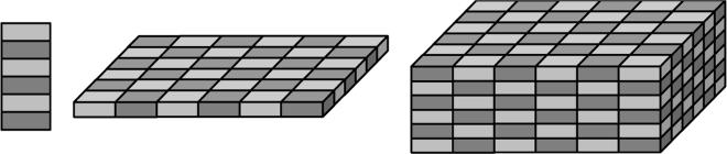
Schematic representations of photonic crystal lattices in 1 (left), 2 (center), and 3 (right) dimensions. Light and dark shadings represent different refractive indices.
The constructive and destructive interference that results from various reflections and refractions of photons within these contrasting materials, and more importantly at the boundaries between them, produce a phenomenon known as photonic bands. A photonic band is a continuous range of light frequencies (of a particular polarization, propagating in a particular direction) that are able to pass through the PhC. A photonic bandgap refers to the range of frequencies of light that cannot pass through a PhC (when propagating with a particular polarization in a particular direction). Photons with frequencies in the bandgap range are only able to penetrate the PhC evanescently and are reflected by the material. The arrangement of appropriate dielectric materials into a properly designed PhC lattice can provide an impressive amount of control over the propagation of light, thus enabling the development of new label-free optical sensing technologies.
2.2 Origin of Photonic Band
The natural starting point in explaining nearly all interesting optical phenomena, including photonic band structure, is with Maxwell's equations. In SI units, they are:
| (1) |
where ρ and J are the free charge and current densities, and E, D, B, and H are the electric, displacement, magnetic induction, and magnetic fields, respectively. All six variables depend on both time and position. For dielectric media that are non-magnetic, non-dispersive, linear, and isotropic, the electric fields E and D and magnetic fields H and B are related through the constitutive relations:
| (2) |
where ε is the dielectric function (of position and time) and ε0 and μ0 are the permittivity and permeability constants of free space. Note that under these assumptions, the refractive index is approximately equal to the square root of the dielectric function, . Combining equations 1 and 2, along with the assumption of harmonic time-dependence at any given frequency, yields the defining equations:
| (3a) |
| (3b) |
where ω is the angular frequency of propagating light. The steady-state distribution of magnetic fields within a PhC, specified by the dielectric function ε(r), is entirely determined by the solution to the differential equation 3a. Electric fields can then be computed using equation 3b.
The photonic band structure described above follows from the solutions to equation 3a. It is an eigenvalue equation, and depending on ε(r), both discrete solutions and bands of solutions may exist. A photonic band exists when equation 3a can be satisfied over a continuous range of frequencies. A photonic bandgap is a continuous range of frequencies for which equation 3a does not have a solution (for the given ε(r)). A discrete solution to equation 3a, corresponding to a specific isolated frequency, describes a confined optical cavity state at that frequency within a photonic bandgap. These discrete solutions are produced by particular geometric defects in the lattice periodicity, as discussed in section 2.5.
Unfortunately, equation 3a cannot be solved analytically for most practical PhC geometries, so researchers instead rely on numerical (computational) modeling to make predictions about the behaviors of various dielectric configurations. However, applying perturbation theory to an electric-field equivalent of equation 3a yields a useful relation when considering the small changes in refractive index that often occur in PhC sensors:
| (4) |
This equation indicates that the fractional change in the frequency of an optical mode of the PhC depends linearly on both the fractional change in refractive index and the fractional portion of electric-field energy in the region where the refractive index is perturbed.10 Since the change in refractive index is typically a property of the analyte being detected, researchers have sought to use the unique properties of PhCs to enhance sensitivity by localizing electric field only to the region where analyte interrogation will occur.
2.3 Photonic Crystal Dimensionality
First analyzed theoretically as early as 1887 by Lord Rayleigh, the multilayer dielectric stack is the simplest example of a 1D PhC.11 Also known as Bragg mirrors, these optical structures consist of alternating layers of high and low refractive index materials. The material composition in these structures is uniform in two dimensions, and periodic in the third: stacked planes with specific thicknesses. They have been used to create commercial coatings and films with engineered transmission and reflection properties throughout the last century. Although not the focus of this review, 1D PhC stacks have been used for sensing purposes; we refer the reader to references [12-20] for more information about them.
Despite the early theoretical foundations for 1D PhCs, the concept of photonic bandgaps existing in two- and three-dimensional structures was not introduced until a century later in separate papers by Yablonovitch21 and John22. Although not physically realizable, the simplest version of a 2D PhC would consist of a dielectric crystal pattern that is periodic throughout a two-dimensional plane, with photon propagation confined only to that plane. In reality, the dielectric materials extend homogeneously into the third dimension. In this respect, two rather different implementations of 2D PhCs exist: PhC fibers and slab-PhCs. PhC fibers approximate the infinitely thick projection of a 2D PhC pattern, and the bandgap properties of the 2D PhC structure are used to guide light along the length of the fiber. While the use of 2D PhC fibers for physical and biochemical sensing has been reported, we will not focus on those structures here and instead refer readers to references [23-25]. Slab-PhCs more closely approximate the zero-thickness case of 2D PhCs. The thickness of the dielectric materials in the third dimension for these devices is typically on the order of the crystal lattice spacing, and light confinement in that direction results from total internal reflection (TIR). Because a significant body of analytical sensing work has been performed using this type of PhC, the bulk of this review will focus on 2D slab-PhCs.
3D PhCs have lattices that exhibit periodicity along all three orthogonal axes. Several examples exist in the natural world, both in geological and biological structures (e.g. opals and iridescent insect scales).26,27 Two common methods of fabricating man-made 3D PhCs are layer-by-layer lithography and colloidal particle self-assembly. Although 3D PhCs are not a focus of this review, such structures are a field of active research both for fundamental purposes and engineered applications like analytical sensing. 3D colloidal crystals, in particular, have been used in various preliminary sensing experiments, and the interested reader is referred to references [15,19,20,28] to learn more.
2.4 2D Slab Photonic Crystals
As described above, slab-PhCs are essentially a 2D periodic array of structural features made from an otherwise uniform thin layer of dielectric material. The propagation of light through a slab-PhC is constrained laterally within the plane of the slab by the photonic band properties of the PhC. Light propagation is constrained in the direction perpendicular to the slab by TIR, so the dielectric layer from which the PhC is made must have a higher refractive index (RI) than the surrounding material. For slab-PhCs that have been implemented in sensing experiments, the dielectric layers thus far have been either polymers or semiconductors (RI > ~1.45) immersed in either a gaseous or aqueous environment (RI < ~1.45). Material composition and fabrication of slab-PhCs is discussed in greater detail in section 4.
There are two common structural arrangements that are most often used in creating slab-PhCs: a lattice of high-RI pillars in a low-RI cover material, and a lattice of low-RI holes in a high-RI slab. Schematic examples of these two geometries are shown in Fig. 2. The photonic bandgaps exhibited by these structures are incomplete; they depend on both the direction and polarization of optical mode propagation within the plane of the crystal. An arrangement of dielectric rods tends to support bandgaps for Transverse Magnetic (TM)-like modes, in which the electric-field vector is predominantly in the direction perpendicular to the PhC plane and magnetic-field vector is predominantly parallel to the PhC plane. The arrangement of holes in a slab tends to support bandgaps for Transverse Electric (TE)-like modes, in which the electric-field vector is predominantly parallel to the plane of the PhC and the magnetic-field vector is predominantly perpendicular to the plane. Because slab-PhCs rely on TIR for vertical confinement, the photonic band properties only apply to guided modes in the slab, and not to light within the light cone that can be radiated from the slab surface.
Fig. 2.

2D slab-PhC geometry schematics representing a square lattice of high-RI pillars (left) and a triangular lattice of low-RI holes in a high-RI dielectric layer (right).
The crystal lattice pattern, the spacing between lattice points (a.k.a. lattice constant), the size and shape of the lattice features, and the RI of cover materials all affect the photonic band structure of a 2D slab-PhC. Because the cover RI and lattice feature size influence band structure, researchers monitor changes in band structure properties (e.g. frequency of a band edge) to make determinations about the materials that infiltrate the slab-PhCs. The photonic band properties of these devices also depend on the thickness of the dielectric slab layer, which is often expressed in terms of the lattice constant. Pillar arrays tend to be 1-5 lattice constants thick, while hole arrays rarely exceed 1.2 lattice constants in thickness. Because lattice constants are often of sub-wavelength dimensions, the thicknesses of the slab-PhCs are also typically smaller than the free-space wavelength of the photons for which they’re designed. The fact that these structures are fashioned from thin planar dielectric layers makes them conducive to fabrication using lithography techniques that are standard in the micro-/nanoelectronics industry, as discussed in section 4. More information about the optical properties of guided modes in slab-PhCs can be found in reference [29].
2.5 Defects in 2D Slab Photonic Crystals
Frequencies of light within a crystal's photonic bandgap are prohibited from propagating through the crystal. A slab-PhC will therefore act as a mirror to photons with a frequency in the bandgap (assuming in-plane propagation and matching polarization). Removing a single lattice point creates a small space that is potentially surrounded by reflecting walls. As long as that new space supports an optical mode with a frequency inside the bandgap, light can become “trapped” there for an extended number of field oscillation cycles. Lattice point removal is not the only modification that causes this effect; perturbing the size or location of one or more lattice points can also cause localized optical modes to resonate in the altered region. As long as there is sufficient spectral separation between supported defect modes in the bandgap, sharp transmission peaks (or dips) at the corresponding frequencies can be observed in the optical transmission spectrum. The frequency of these localized optical resonances is sensitive to refractive index changes within the optical cavity and can therefore be monitored to indicate highly site-specific material interactions. There is significant diversity in the design of these point-like defects in which a region of lattice alterations is surrounded by many periods of unaltered crystal lattice. A selection of these defect designs that have been implemented in sensors is discussed in section 3.
One form of defect has become so ubiquitous in the slab-PhC research community that it warrants further introduction. A photonic crystal waveguide is a defect that is formed by altering a linear sequence of lattice points. For frequencies that are within the bandgap, light is confined to the modified lattice points and therefore propagates along the path of the sequence. This type of defect is used to strategically guide light between two locations within a slab-PhC. Although one of the unique features of PhC waveguides is the ability to make low-loss large angle bends at a single lattice point,30 almost all of the PhC waveguides used in analytical sensors collinearly connect two ridge waveguides at opposite edges of a slab-PhC. In some sensor designs, changes in the photonic properties of the waveguide serve as a transduction signal. Other sensor designs use the waveguide to route light either to and from a heterostructure defect or to side-couple light to point-like defects (as described later in section 3.2). In many cases the PhC waveguide enables a transmission spectrum to be recorded for light passing through the PhC sensor.
Although a number of different lattice point modifications have been used successfully in making PhC waveguides, the most common waveguide is the “W1” waveguide, where an entire row of holes is left filled in.31,32 Another commonly used waveguide is the slotted-photonic crystal waveguide, in which a thin line of dielectric material is removed along the center of a W1 waveguide over its entire length.33 SEM images of both the W1 waveguide and slotted-PhC waveguide are presented later in section 3.2 of this review.
2.6 1D Slab Photonic Crystals
There are several other sensor designs that rely on the photonic band properties produced by modification of a thin planar dielectric. While not covered in detail here, two of the most widely studied (a 1D grating PhC, and a periodic waveguide PhC) only apply periodicity in one dimension. In the first type, a periodic dielectric pattern is established along one planar direction, but the pattern is uniform in the perpendicular planar direction to create a planar grating. These 1D grating PhCs operate as reflectometric sensors.34 The second type creates a photonic crystal pattern in a ridge waveguide, relying on total internal reflection (TIR) to confine light in two directions and the PhC properties to control light propagation along the length of the PhC waveguide.35 Other devices that have recently been used for sensing purposes cloud the distinction between 1D and 2D PhCs. Referred to as a photonic crystal slot nanobeam waveguide,36 and quadrabeam photonic crystal cavity,37 these sensors respectively incorporate two and four adjacent suspended 1D beam-PhCs to create strong field localization in the slots between them.
3 Sensor Design
Among the 2D-slab PhC analytical sensors that have been used to make experimental measurements to date, there is significant diversity in sensor design. This diversity exists in both the measurement methodologies and in the physical geometries of the actual PhCs. In this section, we first review the various measurement schemes that have been implemented to monitor physical or chemical changes within PhCs. We then present a brief summary of the various geometrical configurations of 2D-slab PhCs that have been used for analytical sensing.
3.1 Methods of Measurement
The strong optical resonances that can be achieved in slab-PhC cavities have made them useful when implemented both in sensors with passive optical cavities and those integrating active gain media. For active cavities, source light is used to optically pump a gain medium, and laser emission from the cavity is measured. In this case, propagation of the input (pump) and output (emission) light is predominantly perpendicular to the plane of the slab. For PhCs with passive cavities, the incident source light is simply reflected from, transmitted through, or re-directed by the PhC cavity before being measured as output. Adding to the diversity of design for passive slab-PhC cavities, the direction of light input into the PhC can be oriented either perpendicular to the slab or parallel to the slab through in-plane waveguiding. Output light for slab-PhCs with passive cavities can also propagate either perpendicular (radiated) or parallel (waveguided) to the plane of the slab. Fig. 3 displays a rough taxonomy of slab-PhC sensor measurement schemes. In this subsection, we first discuss measurement using active-cavity PhCs, then perpendicularly illuminated passive PhCs, and finally PhCs with in-plane illumination.
Fig. 3.

Taxonomy of experimental measurement schemes relating to the input and output light in 2D slab-PhCs.
All optically active slab-PhC sensors share a similar measurement methodology. Pump illumination is shined on one or more layers of III-V semiconductor quantum structures embedded within the PhC, and the outward radiating stimulated emission is collected and analyzed. Because the emission wavelength is dependent on the RI of the low-RI regions of the PhC, shifts in emission wavelength indicate material changes within the PhC. Both planar quantum well layers38-43 and embedded quantum dots44,45 have been used in this configuration to make measurements.
To increase the number of measurements and eliminate the need for a spectrometer, Kita et al. suggested combining an array of PhC nanolaser structures with a band pass filter and InGaAs camera.39 With this set-up, target binding induces an emission shift across the filter edge wavelength so that the illumination passes from the nanolaser to the camera, allowing a large number of individual binding sensors to be simultaneously monitored.
The approach to measurement wherein both the input and output light propagates predominantly perpendicular to the 2D PhC slab surface is not exclusive to devices using active gain media. Several research groups have made measurements by illuminating a passive 2D PhC slab surface and then observing the reflected or transmitted light radiating perpendicularly from the slab. As with active PhC sensors, it is the spectrum of reflected or transmitted light that is often analyzed. In one approach, researchers monitored changes in overall intensity of a broad reflection peak;46-50 in another, changes in the reflectance spectrum were monitored.51 Huang et al. also monitored shifts in the wavelengths of spectral features, but for transmitted light.52 In an alternative measurement scheme, Amsden et al. recorded the angular spectrum of light diffracted through the PhC plane before and after chemical surface modification.53 Expanding the scale of parallel measurement of single binding events, Grepstad et al. collected images of a large PhC region illuminated at the wavelength of a transmission minimum. In that setup, bound nanoparticles caused enhanced local transmission and thus appeared as bright spots in the PhC image.54
Compared with a measurement scheme in which passive slab-PhCs are perpendicularly illuminated, many more sensors have been designed so that input light is guided within the plane of the PhC. Significant diversity exists in the specific PhC geometry among this group of sensors and is discussed in the next subsection. The input light is most often coupled into waveguide structures using an end-fire method through a tapered fiber or high-NA microscope objective, although grating couplers have also been used. The collection of output light then depends on whether the in-plane transmitted light or the free-space radiated light is being monitored for sensing purposes. If the in-plane transmitted light is being monitored, then it is coupled out of the chip via end-fire coupling and monitored with a either photodetector or optical spectral analyzer (OSA).55-82 Photodetectors are used when the incident light source is a tunable laser, and OSAs are used in conjunction with broadband LED or supercontinuum laser sources. If free-space radiated light is being monitored, then it is collected with a microscope objective and analyzed with a photodetector or CCD camera.65,83
3.2 Photonic Crystal Sensor Geometry
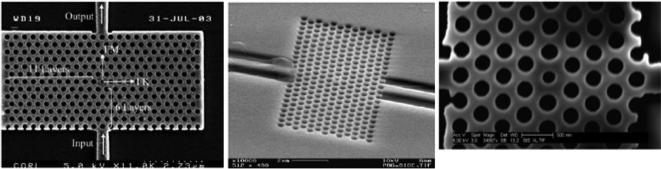
Although there is great diversity in the geometrical design of 2D slab-PhC sensors, they all share one defining trait: an in-plane photonic bandgap that results from 2D periodicity in the arrangement of dielectric material. While most of the sensors utilize a periodic array of holes (lower RI) in a dielectric slab (higher RI), arrays of high-RI pillars in a low-RI cover material have also been used. Several sensors have been used to make measurements in which there are no defect structures or inherent alterations to the periodicity of the crystal.46-54,67,84 Example SEM images of some of these structures are shown in Fig. 4.
Fig. 4.

SEM images of 2D slab-PhC sensors with uninterrupted lattice periodicity. Note that a triangular lattice is shown in (a), while (b) shows a uniform square lattice pattern. The checkerboard lattice shown in (c) employs two holes of differing radii in each unit cell. Also note that light transmission was in-plane for the PhC in (a), but entirely perpendicular for (b,c). (a) Scale bar 1 μm. From ref. [67] with permission from AIP Publishing LLC., copyright 2010. (b) From ref. [52] with permission from The Optical Society, copyright 2009. (c) From ref. [84] with permission from The Optical Society, copyright 2013.
The various defects and modifications that can be applied to the requisite structural periodicity of a 2D PhC were introduced in section 2.5. The remaining designs that will be discussed in this section rely on one or more of these alterations to the PhC periodicity in order to create specific features in the transmission or radiation spectrum that shift when there is a RI change within the PhC structure. For convenience, various PhC geometries will be discussed according to the following groupings: isolated point-like cavities, waveguide cavities, and point-like cavities that are side-coupled to waveguides.
For the purpose of this review, an isolated point-like cavity is any modification to an otherwise uniform periodic lattice that is completely surrounded by that uniform lattice, without being side coupled to a PhC waveguide. The simplest example of a point defect is a single modified lattice point. In references [56,58,66] the reduced radius of a single hole in a triangular lattice (see Fig. 5) resulted in electric field localization around that lattice point. Another common approach is to simply remove lattice points. This strategy was followed by Chakravarty et al., who removed a line of four adjacent holes from a triangular lattice to create what is known as an L4 cavity.44 A third common technique for creating optical cavities is to simply translate the location of lattice structures within the plane of the PhC. This approach was used by Kita et al. where the positions of four lattice holes in a triangular lattice were displaced outward away from the center point between them, as shown in Fig. 6.39 An isolated optical cavity spanning a larger number of lattice points was used by Xu et al. when concentric rectangular regions of a face-centered cubic lattice of pillars were given slightly different lattice constants,70 as shown in Fig. 7. Other isolated point-like cavities have been created by using a combination of changing lattice point size, location, and even shape.39-41,43,45,59,62,76 A sample of these geometries is shown in Fig. 8.
Fig. 5.
SEM images of PhC sensors in which a single lattice hole has a reduced radius size. (left) From ref. [56] with permission from The Optical Society, copyright 2004. (center) From ref. [58] with permission from The Optical Society, copyright 2007. (right) From ref. [66] with permission from Elsevier, copyright 2009.
Fig. 6.
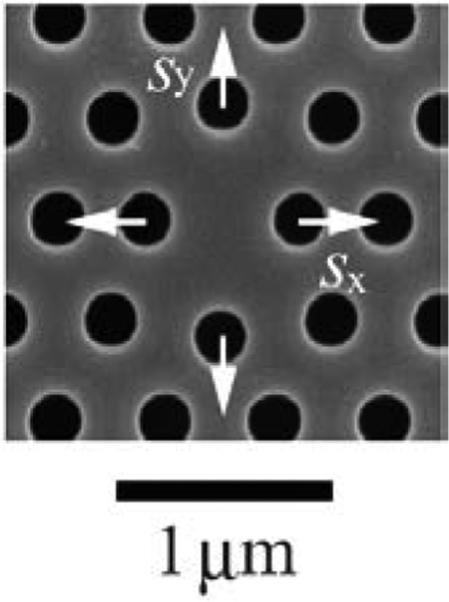
SEM image of a PhC design utilizing translated lattice points to create a localized optical cavity. From ref. [39] with permission from The Optical Society, copyright 2008.
Fig. 7.

SEM Image of a PhC design utilizing concentric regions of differing lattice constants. From ref. [70] with permission from The Optical Society, copyright 2010.
Fig. 8.

SEM images of various PhC designs with point-like cavities. Note the various lattice symmetry alterations used in creating localized cavities: lattice point size (a-e), lattice point location (c), lattice point deletion (b-d), lattice point shape (e). (a,b) From ref. [45] with permission from The Optical Society, copyright 2010. (c) From ref. [76] with permission from The Optical society, copyright 2012. (d) From ref. [59] with permission from The Optical Society, copyright 2007. (e) From ref. [38] with permission from AIP Publishing LLC., copyright 2003.
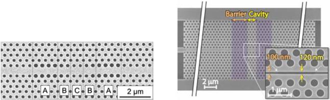
As described in section 2.5, PhC waveguides can be constructed by modifying or removing an entire lattice row from a PhC. The sensors considered in this and the next paragraphs all utilized that basic structure either alone, or in combination with other structural changes in order to confine light within a localized region of the PhC waveguide. For this group of sensors, the simplest design is the one in which the only modification is the removal of a single row of lattice points. This approach was taken by various research groups in order to measure surface binding of small molecules.57,63,68,69 In a slightly different version of this sensor design, a waveguide is created by reducing the radii of a line of lattice points rather than removing those points completely.55,63 SEM images of both types of designs are shown in Fig. 9. Another waveguide design further modifies the standard W1 waveguide by inserting a long line-defect along the length of the PhC where a row of lattice points has been removed. This slot-waveguide structure is applied to increase the interaction between analyte in the cover material and the electric field carried within the waveguide.85 Lai et al. have used this sensor design, shown in Fig. 10, to make separate measurements in both gases and liquids.72,73
Fig. 9.
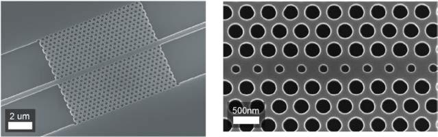
SEM images of W1 waveguide (left) and modified W1 waveguide (right) PhC designs. From ref. [63] with permission from The Optical Society, copyright 2008.
Fig. 10.

SEM image of a slotted PhC waveguide sensor design. From ref. [72] with permission from The Optical Society, copyright 2011.
By making modifications around a short section of either the basic W1 waveguide or its slotted equivalent, researchers have been able to confine light to within that local region for sensing purposes. These devices are often described as waveguide heterostructure cavities. In the simplest of these experiments, a wetted glass microtip was dragged over an otherwise unmodified W1 waveguide (see Fig. 11). The liquid infiltrated the PhC lattice holes due to capillary adhesion, and the RI perturbation along that section of the waveguide allowed the formation of a more localized optical cavity for analysis of the liquid.60 In other designs, the radii or positions of only a few lattice holes adjacent to a W1 waveguide were varied in order to create localized optical cavities.65,80,83 Similarly, heterostructure cavities were designed in slotted PhC waveguides by modifying the slot width86 or lattice constant64,74 along a short region of the slotted waveguide.85 SEM images of waveguide and slotted-waveguide heterostructure sensor designs are shown in Fig. 12.
Fig. 11.
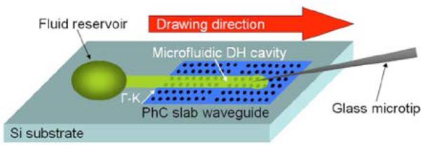
Schematic image of a waveguide heterostructure sensor design in which a localized optical cavity is caused by fluid infiltration. From ref. [60] with permission from The Optical Society, copyright 2008.
Fig. 12.
SEM images of waveguide heterostructure sensor designs in which localized optical cavities result from altered radii of lattice holes adjacent to the W1 waveguide (left) and varied width of a slot-defect (right). (left) From ref. [83] with permission from AIP Publishing LLC., copyright 2008. (right) From ref. [86] with permission from The Optical Society, copyright 2010.
The last grouping of sensor designs described here are the point-like cavities that are side-coupled to PhC waveguides. All of these designs have a point-like PhC cavity (surrounded by lattice structures on all sides) within a few lattice constants of a W1 waveguide, and they rely on the evanescent penetration of light from the waveguide to the cavity for confinement. Much like the point-like optical cavity designs already discussed, two common design techniques for waveguide side-coupled cavities are to remove lattice structures61,65,78 or change the size of lattice structures.61,65 Other designs incorporate a combination of lattice structure modifications including removal, altered size, altered position, and even insertion of other much smaller features.71,77,79,81,82 SEM images of some of these sensors are shown in Fig. 13.
Fig. 13.

SEM images of sensor designs in which a point-like defect is placed within the vicinity of a bus W1 waveguide to allow evanescent side coupling from the waveguide to the cavity. (left) From ref. [79] with permission from Elsevier, copyright 2012. (right) From ref. [65] with permission from Elsevier, copyright 2009.
4 Fabrication
For slab-PhCs to have photonic band properties at visible and IR wavelengths, the size of and spacing between structural features is typically on the order of hundreds of nanometers or less. Since most of the existing slab-PhC sensors are fabricated in semiconductor substrates, many of the fabrication techniques that are commonly used also carry over from the semiconductor electronics industry, where such feature sizes have been standard for decades. Although less common, innovative soft-lithography techniques have also been used to fabricate slab-PhCs in polymer-based materials.
4.1 Semiconductor-based Slab Photonic Crystals
The choice of substrate for semiconductor-based slab-PhCs depends on whether an active or passive optical cavity is used. The slab material must provide optical gain for active cavity devices, so compound semiconductors are chosen because of their desirable electronic band properties. For these types of devices, III-V alloys like GaAs or InGaAsP are typically used. Silicon based substrates (Si or SiN) are most often used for passive optical cavity sensors, although compound semiconductor alloys are also compatible. The most common substrate used for passive cavity slab-PhCs is silicon-on-insulator (SOI), in which a thin device layer of Si (< 500 nm) is situated on top of a thicker layer of SiO2. Nearly all passive-cavity slab-PhCs operate at IR wavelengths, although some SiN devices can potentially operate at visible wavelengths.
Regardless of the specific device material substrate, the general process of fabrication is similar for all semiconductor slab-PhCs. The PhC pattern is first written using some form of lithography before being transferred to the device layer via an etching technique. The most common method used for PhC sensor pattern exposure is electron beam (e-beam) lithography. E-beam pattern writing is commonly used in literature-reported devices despite its relatively high cost and slow speed due to its versatility in the prototyping process: no expensive photolithography masks need to be prepared. An e-beam-sensitive resist is first deposited on the substrate surface, and then a highly focused beam of electrons is used to write a pattern by serially scanning across desired pattern areas. Photolithography is another exposure method that can be used for pattern writing. In this parallel process, the pattern is first defined in a photomask. UV light is shined on the mask, and light transmitted through the mask interacts with the resist to either strengthen or weaken the material. Although more efficient and significantly cheaper for mass production, photolithography poses greater initial costs and no iterative design flexibility. For any slab-PhC sensor to be produced at commercial distribution scales, pattern writing must be achievable through photolithography. In either type of lithography, developing the resist removes either the exposed or unexposed areas of resist depending on whether the resist tone is positive or negative, respectively. The developing step leaves a mask layer of resist with the particular pattern that will be transferred to the substrate beneath it.
The PhC pattern is transferred from the resist layer to the device layer by chemical etching. Dry chemical etch processes (reactive ion etch (RIE) or inductively coupled plasma (ICP) etch) are the most common, although wet chemical etches have also been used. For some slab-PhC designs, the dry etch used to transfer the pattern to the device layer is followed by a wet etch to remove the layer underneath and leave a suspended device layer. In certain fabrication protocols, the PhC pattern is first transferred from the resist mask to a hardmask layer (e.g. SiO2) on top of the device layer through an initial etch process, and then an additional etch is used to transfer the pattern to the device layer itself.
4.2 Polymer-based slab Photonic Crystals
While semiconductor substrates are typically used for slab-PhC sensing devices, designs have also been reported in which periodic PhC patterns are produced in thin polymer layers. For one such sensor, nanoimprint lithography (NIL) was used to heat-transfer a periodic pattern of sub-micron features to a cyclo-olefin polymer film over areas spanning tens of square centimeters.46,47 While limited details were provided on the method, the authors highlighted that NIL is a low cost, high throughput production process.46 Although outside the context of sensor development, fabrication of planar PhCs using NIL is also presented in references [87,88]. In another device, a solution containing silk fibroin was poured over a master mold (with the inverse image of the PhC pattern) and allowed to dry.53 In both cases, the patterned polymer films were separated from the mold after curing; the mold could be re-used. It is worth noting that the molds for these polymer PhCs are fabricated using standard lithographic techniques discussed in section 4.1. It should additionally be noted that, while not reported for use as sensors, planar PhCs have also been fabricated using soft-lithography89 and multi-photon polymerization90,91 methods.
5 Experimental Approach
Regardless of device design and measurement format, the sensitive, specific, and reproducible detection of biomolecules using slab-PhCs requires a strategy for viable attachment of the probe molecules at the sensor surface. Additionally, the assay format employed for the delivery of target molecules to the probe immobilized crystal surface can have a considerable effect on detection limit, assay time and the amount of target sample required. In this section, we will discuss various surface chemistry strategies employed for attaching probe molecules to slab-PhCs along with the two widely used assay formats for target delivery.
5.1 Surface Chemistry
While the sensing mechanism of a slab-PhC device relies on the engineered optical properties of the PhC geometry, capturing the intended target that will be detected at the sensor surface still requires traditional surface functionalization steps. Detection of biomolecules, in particular, has often been realized by covalently attaching ligands (e.g. antibodies) to the photonic crystal surface and subsequently capturing the target of interest. A broad range of surface functionalization and probe molecule immobilization strategies have been developed by the biosensor community.92-95 While most of these are common to different sensor formats, it is nevertheless worthwhile to review these strategies in regard to slab-PhCs. Thus far, functionalization of most SOI-based photonic crystals has begun with the attachment of aminoalkoxysilanes to the oxide surface. This chemistry provides terminal amine groups so that biomolecules can either be attached directly or the surface can be further modified for the attachment of biomolecules. Either 3-aminopropyltriethoxysilane (APTES) or 3-aminopropyldimethylethoxysilane (APDMES) has been utilized to modify the PhC surface with amine groups.50,74,75,77,79,80,82,96 These surfaces are further modified using glutaraldehyde or N-hydroxysuccinimide-biotin (NHS-biotin). In the former case, one end of glutaraldehyde reacts with the surface amines and other end reacts with the primary amines typically found on the surface of proteins and peptides by imine formation, therefore covalently capturing biomolecules at the surface. In the latter case, NHS-biotin reacts with the amines on the surface and attaches the biotin by forming a stable amide bond. Once the biotin is attached to the surface, streptavidin labeled probe molecules are immobilized directly, or biotin-labeled probes are immobilized via an intervening streptavidin layer. These two surface chemistries are represented in Fig. 14.
Fig. 14.

Example surface functionalization strategies used for capturing probe molecules after modifying the oxide surface with 3-aminopropyltriethoxysilane (APTES). a) Amine terminated surface reacts with glutaraldehyde resulting in an aldehyde terminated surface that can react with the primary amines present on the surface of probe molecules resulting in their covalent capture to the surface. b) NHS-biotin reacts with the amine terminated surface for the specific capture of streptavidin. Biotinylated probe molecules can be captured specifically by this streptavidin modified surface.
In another functionalization scheme, Buswell et al. used mercaptopropyltrimethoxysilane to modify the oxide surface of their crystals before biotin was covalently attached to the surface via disulphide bond formation.63 Zlatanovic et al. used (trimethoxysilylpropyl) ethylene diamine triacetic acid to terminate the PhC surface with carboxylic acid groups.66 These terminal groups were activated using 1-ethyl-3-(3-dimethylaminopropyl)carbodiimide/N-hydroxysuccinimide (EDC/NHS), following which, biotinylated bovine serum albumin was immobilized to the surface via amide bonds. In the case of GaAsInP photonic crystals, Kita et al. modified the surface of their PhCs initially with N-2-(aminoethyl)-3-aminopropyltrimethoxysilane and subsequently with glutaraldehyde.40 After modifying the surface with chemical moieties, bovine serum albumin (BSA) was immobilized on the surface. Lu et al. adsorbed BSA on the surface of GaAsInP crystals after modifying the surface with 1-octadecanethiol.41 These chemical functionalization schemes are all represented in Fig. 15.
Fig. 15.

a) Oxide surface is modified with 3-isocyanatopropyltrimethoxysilane to produce an amine reactive surface. The isocyanate groups react with amines on the surface of probe molecules resulting in their covalent capture. b) Oxide surface is modified to produce carboxyl group terminated surface. Upon activation of these groups with EDC/NHS, probe molecules can be captured covalently. c) Mercaptosilane is used to obtain a thiol modified surface. Subsequently, biotinylated probe molecules in the presence of DMSO can be covalently captured by this surface.
5.2 Analyte Delivery
In sensing experiments with biomolecules, slab-PhC sensors have been used either in an end-point assay format or integrated into lab-on-a-chip (LOC) devices. In the former case, the capture probe-modified PhCs are incubated with a solution containing the target of interest before they are subsequently washed, dried and optical spectra are collected. LOC devices allow for real-time binding interactions to be monitored between the ligand and target in a microfluidic environment by simultaneously collecting optical spectra.
In the end-point assay format, the PhC chip is dry when the optical spectrum is collected. The high contrast in RI between the target analyte and air is significantly larger than between analyte and water, so a larger resonance change is observed for any given analyte on a dried sensor. Research groups have used this assay format to detect proteins, DNA, influenza virus and virus-like particles. More details regarding specific examples will be discussed in section 6.
On the other hand, integration of microfluidic channels with photonic crystals offers unique advantages. In addition to the potential for measuring binding interactions in real time, microfluidic channels accommodate small sample volumes (e.g. sub-microliter), a potentially crucial feature when analyzing precious samples. The footprint of most photonic crystals is on the order of tens of square microns, suggesting that individual crystals on a single chip can be uniquely addressed using microfluidic channels, thus facilitating multiplexed detection.
Soft lithography techniques employing an elastic polymer, typically polydimethylsiloxane (PDMS), are commonly used for fabricating microfluidic channels. The lithography molds required for this process are fabricated using standard microfabrication techniques (see section 4.1). Researchers have used PhCs integrated with microfluidic channels for real-time detection of anti-biotin66 and avidin,74 as will be discussed in section 6.2.3.
6 Experimental Results
Slab-PhCs have been used to detect changes in the RI of bulk media such as liquids and gases and also changes in RI at the sensor surface induced by adsorption of either chemical or biological molecules. In this section, we will provide an in-depth summary of the reported sensing results related to both bulk material and local surface RI changes.
6.1 Bulk Refractive Index Measurements
The primary transduction mechanism in most slab-PhCs is the shift in mode resonance that occurs when part of a resonant optical mode interacts with a sample of interest. An overall change in the bulk refractive index (Δn) due to the presence of a target analyte, when compared to a reference cover material, is perhaps the most basic sensing operation achieved by slab-PhC sensors. The bulk RI sensitivity, defined as a change in the resonant wavelength for a unit change in the bulk refractive index (Δλ/Δn; nm/RIU) is therefore widely used as a performance metric for comparing different slab-PhC designs.
6.1.1 Bulk RI Measurements of Liquids
Many research groups have determined the bulk RI sensitivity of their PhC sensors by monitoring the changes in optical properties that result from incubating their sensors with liquids of different RI values. First, the sensitivity of PhCs with passive point-like optical cavities will be considered. Chow et al. reported a sensitivity of 200 nm/RIU with a single reduced-radius lattice-point defect optical cavity using five silicon fluids with refractive indices ranging from 1.446 to 1.454 with increments of 0.002 RIU.56 Based on the noise level in the measurement system, they estimated the detection limit of their device (Δn) to be better than 0.001 RIU. Zlatanovic et al. determined the bulk RI sensitivity of slab-PhCs with a point-like cavity to be between 161-176 nm/RIU based on the shift in the resonant wavelength for both water and silicon oil from air for 19 such crystals.66 They attributed the variation in the sensitivities to changes in the fabrication process. Liu et al. demonstrated a RI sensitivity of 460 nm/RIU with a slab-PhC in which three pairs of small holes of differing size and lattice constant were fabricated along an L7 cavity.76 This was established by measuring the shift in the resonant wavelength between ethanol and water. Xu et al. reported a sensitivity of 350 nm/RIU with a pillar-based optical microcavity by using six optical fluids with RI values ranging from 1.392 to 1.442 with increments of 0.01 RIU.70 Based on the full-width-half-maximum of the transmission peaks, the estimated index resolution of their device was 3 × 10⁻⁴ RIU.
Several research groups have used slab-PhCs with point-like optical cavities that utilize active gain materials for stimulated emission in order to make bulk RI sensitivity measurements. Lončar et al. demonstrated a sensitivity of 176 nm/RIU by measuring the wavelength shifts for IPA and methanol with respect to air using a PhC nanocavity sensor.38 Kita et al. demonstrated a sensitivity of 350 nm/RIU with their slab-PhC device using liquids with RIs ranging from 1.00 to 1.37, and they reported the minimum detectable change in RI to be 9 × 10⁻⁵ RIU.39 Kim et al. used index-matched liquids at five different refractive indices ranging from 1.296 to 1.373 in increments of 0.019 and reported a sensitivity of 135 nm/RIU with an estimated RI resolution of 0.001 RIU for their slab-PhC.40 Dündar et al. used different concentrations of sugar-water solutions to determine the sensitivity of their slab-PhC to be 280 nm/RIU.45
Designs that implement only a PhC waveguide have also been used for sensing bulk RI changes. Skivesen et al. used a W1 waveguide slab-PhC and reported a sensitivity of 64 nm/RIU.57 The RI sensitivity was determined by measuring the shift of the bandgap cut-off wavelength for water and two immersion oils with RI values of 1.33, 1.48 and 1.518, respectively. These RI values for the liquids were measured at λ = 630 nm, although the cut-off wavelength of the crystal is ~1500 nm. Therefore, the authors suggested a ~1% offset in the shifts in the resonant wavelength upon considering dispersion corrections. Buswell et al. observed a sensitivity of 88 nm/RIU for a W1 waveguide PhC design.63 Modification of their design by adding a row of holes with radius smaller than the normal lattice holes along the W1 waveguide provided a sensitivity of 120 nm/RIU, a 40% improvement. The improved sensitivity was attributed to the higher surface area available for sensing in the region of high field confinement. Lai et al. used a PhC slot waveguide as a near-IR absorption spectrometer to observe xylene-water signatures.73 Differences in the intensity of light transmitted through the slab-PhC in the presence and absence of the target solution were used to calculate the absorbance of the analyte using Beer-Lambert law. With this methodology, the authors observed a good correlation between the experimentally determined absorbance spectrum of xylene in water and the theoretical spectrum. A detection limit of 100 ppb or 86 μg/L was reported for the detection of xylene in water using their device.
Some waveguide heterostructure PhC designs have also been characterized using bulk RI sensitivity measurements. Bog et al. demonstrated narrow transmission resonances for a waveguide heterostructure cavity created by infiltrating microscope immersion oil (n = 1.50) into a narrow region of the PhC waveguide.60 Without measuring the shift in the transmission resonances of the device for two different fluids, based on a single measurement and numerical calculations, they estimated the sensitivity and detection limit of their sensor to be 60 nm/RIU and 4.5 × 10⁻⁴ RIU, respectively. By immersing a width-modulated-cavity (WMC) design of slab-PhC in air, water, and IPA, Dorfner et al. reported a sensitivity of 103 ± 1 nm/RIU.65 Pal et al. observed a sensitivity of 64.5 nm/RIU using a W1 heterostructure slab-PhC by monitoring the resonant wavelength in air, water and isopropylalcohol (IPA).75 This device was found to have a detection limit of Δn/n = 10−2. Later, a Peltier thermo-electric cooling module was incorporated beneath the PhC to eliminate temperature-induced shifts in the resonant wavelength. This was necessary as silicon has a small, non-negligible thermo-optic coefficient.97 The temperature sensitivity of the resonance for that PhC sensor was subsequently determined to be 0.1 nm/K, supporting the use of temperature control in subsequent measurements.98 Di Falco et al. used caster sugar solutions with RI values ranging from 1.315 to 1.340 to determine the bulk RI sensitivity of their slotted-waveguide heterostructure cavity design.64 The RI values of caster sugar solutions were determined at the wavelength of the resonant mode (1550 nm) using a refractometer. For the three different concentrations of caster sugar solutions used, a sensitivity of 1538 nm/RIU was obtained; to our knowledge, this is the highest bulk RI sensitivity value reported for any slab-PhC device.
The slab-PhC structures in which point-like cavities are side-coupled to the PhC waveguide have also been implemented for sensing the RI of liquids. Dorfner et al. characterized the bulk RI sensitivity of two crystal designs: L3 and H1 (radius of a single hole is larger than the crystal lattice holes) cavities side coupled to a W1 waveguide.61 By monitoring the shift in the resonant wavelength of both these crystal structures for water and IPA from air as a reference, sensitivities of 63 nm/RIU and 155 nm/RIU were reported for the L3 and H1 cavities, respectively. Kang et al. reported RI sensitivity values of two crystal designs, both modifications of an L3 cavity.71 They measured the wavelength shift when air in the crystal was replaced with silicon oil. Observed sensitivities for the two cavity designs were 91 nm/RIU and 98 nm/RIU. Lai et al. demonstrated a sensitivity of 52 nm/RIU with a W1 side-coupled L13 PhC design by measuring the shift in the resonant wavelength for IPA from water.78 The same group later reported an improved sensitivity of 66 nm/RIU for the L13 cavities after modifying their PhC design to increase the group index of the propagating light in the W1 waveguide.81
Bulk RI sensitivity measurements have also been made for passive slab-PhCs in which the illumination is perpendicular to the plane of the PhC. A suspended slab- PhC design fabricated by Huang et al. was shown to have a bulk RI sensitivity of 510 nm/RIU.52 This was demonstrated by monitoring the resonant wavelength for the device in air, water, IPA and IPA-chloroform mixture. A nanopatterned 2D periodic crystal fabricated from silk protein has also been used for bulk RI sensing.53 RI changes in the vicinity of the crystal resulted in a colorimetric shift of light diffracted through the periodic structure. Because of this, the authors noted that their device could be used in either a qualitative or a quantitative mode. The bulk RI sensitivity was measured to be 400 nm/RIU after observing the spectral shifts for various concentrations of glucose solution, ranging from 0% to 40%. The data also suggested a bulk RI resolution of 0.007 RIU for the device. Nicolaou et al. reported a bulk RI sensitivity of a checkerboard photonic crystal slab design to be 832 nm/RIU.84 This was achieved by monitoring the position of the resonant wavelength of the device for three different liquids of known RI values.
6.1.2 Bulk RI Measurements of Gases
In a few cases, slab-PhCs have also been used for sensing gases. Sünner et al. demonstrated a sensitivity of 80 nm/RIU for their W1-coupled heterostructure cavity design by measuring the resonant wavelength of the crystal in helium, nitrogen, argon and sulfur hexafluoride in a temperature controlled environment.83 Jágerská et al. employed a slotted W1 waveguide heterostructure cavity for sensing gases and measured a sensitivity of 510 nm/RIU using air, helium, carbon dioxide and nitrogen.86 The RI values of the gases used in the study were calculated for λ = 1570 nm at atmospheric pressure and room temperature using ideal gas law. The precision of the resonance peak was determined to be ± 3 pm, suggesting a detection limit of 1 × 10⁻⁵ RIU for this crystal design. Using their PhC slot waveguide structure, Lai et al. performed near-IR absorption spectroscopy of methane and reported a detection limit of 100 ppm.72 Using a fluid incorporated PhC waveguide crystal structure, Casas-Bedoya et al. demonstrated humidity sensing.99 The ionic liquid that infiltrated all the lattice holes of the device had a refractive index which varied with the relative humidity (RH). Authors suggested that an increase in the RH could increase the pressure at the liquid surface, therefore reducing the liquid volume within the lattice holes, and thus affecting the RI of the crystal structure. A combination of both these effects was attributed to the observed shifts in the cut-off wavelength of the slab-PhC with changes in the RH within the chamber. This study demonstrated the utility of slab-PhCs as on-chip compact humidity sensors.
6.2 Protein Sensing
As previously mentioned, slab-PhCs can be operated either dry (the sensor is rinsed and dried following incubation with an analyte solution) or in one of two wet formats (either static, or as part of a flow-through, “lab-on-a-chip” device). Detection of proteins has been accomplished using all three of these formats.
6.2.1 Dehydrated Protein Layers
Since the detection mechanism for a slab-PhC depends on a change in RI in a region that is local to the sensor surface, a greater index contrast between the biomolecules and the cover material of the crystal will offer better sensitivity. Drying sensor chips after analyte exposure but before spectrum measurements in air maximizes the index contrast (Δn ~ 0.45) ensuring enhanced resonance change and improved sensitivity.
One of the earliest demonstrations of detection of dehydrated protein layers using slab-PhCs was reported by Lee et al.58 In this study, non-specific, covalent binding of BSA molecules to a glutaraldehyde-modified sensor surface was demonstrated using a slab-PhC with a point-like cavity. Considering the net red-shift in the resonant wavelength for the BSA layer and the surface area available for its binding, the calculated minimum detectable amount reported was 2.5 fg. Additionally, a proof-of-principle demonstration for specific detection of streptavidin using immobilized biotin as the capture probe was presented, without any mention of the detection limit. Specific detection of biomolecules using a slab-PhC was subsequently reported by Buswell et al.63 This was achieved by immobilizing biotin to a 3-mercaptopropyltrimethoxysilane modified surface of the waveguide slab-PhC, and then incubating the chip with a 10 μM solution of streptavidin. Based on ellipsometric measurements from a separate experiment, the thickness of the streptavidin layer was determined to be 2.5 nm. Without reporting detection limits, the authors mentioned that a 0.86 nm shift in the band cut-off wavelength could be expected for a 2.5 nm thick protein layer with their slab-PhC design.
Using a point-shifted nanocavity laser, Lu et al. detected adsorption of BSA to a 1-octadecanethiol modified crystal surface.41 Briefly, 1 mg/mL of BSA was allowed to adsorb for an hour; subsequently, the chip was rinsed and dried before collecting the spectrum. Adsorption was then monitored using three lasing modes of the crystal: monopole, whispering gallery (WG) and dipole modes. Net shifts in the resonant wavelength were observed in each case. Considering the surface area of the crystal with strong electric field confinement, 2.2 fg was the estimated limit for mass detection. Further, considering the spectral line width of the WG mode (0.6 nm), the calculated mass sensitivity of the device was reported to be ~0.8 fg.
Pal et al. demonstrated antibody-mediated, specific detection of human IgG (hIgG) using a W1 waveguide heterostructure design.75 The crystal surface was chemically modified with APDMES and GA, and the probe molecule, anti-hIgG, was subsequently immobilized. Following this, different concentrations of hIgG in 10-fold dilutions (6.7 μM to 0.67 nM) were tested. Based on the dose-response curve generated for observed shifts in the resonant wavelength for each tested concentration, a dynamic range of over 3 orders of magnitude and a detection limit of 6.7 nM for hIgG were reported. A calculated concentration sensitivity of the device was determined to be (2.3 ± 0.2) × 105 nm/M. Moreover, a Langmuir isotherm was fit to the dose-response curve and the equilibrium dissociation constant, KD, for the probe-target pair was determined to be 7.2 × 10⁻⁷ M, which is within the range of the values reported in the literature. Considering the surface area of crystal device where more than 50% of the electric field was confined and the lowest detectable concentration of hIgG, the estimated minimum detectable mass of hIgG was reported to be 1.5 fg. Furthermore, error-corrected (redundant) detection of proteins was successfully demonstrated for the first time by simultaneously monitoring the shifts in the resonant wavelength for three crystals upon specific binding of hIgG to the slab-PhCs. This also indicated the potential for multiplexed detection, provided individual crystals could be immobilized with unique probe molecules.
Using a cyclo-olefin polymer-based slab-PhC, Terada et al. demonstrated specific detection of concanavalin A (Con A) binding to surface immobilized glycopolymers, namely, mannose homopolymers (ManHP) and mannose -incorporated nanogel particles (ManNP).49 By monitoring the change in the intensity of the reflected light from the PhC, detection limits of 16.7 ng/mL and 6.0 ng/mL were reported for ConA binding to ManHP and ManNP, respectively. The lower detection limit in the case of ConA binding to ManNP was attributed to the three-fold increase in the binding capacity of nanogel particles in comparison with ManHP immobilized directly on the slab-PhC. This study establishes the utility of slab-PhCs for detecting specific interaction between proteins and sugars.
6.2.2 Protein Sensing in a Static Aqueous Environment
Detection of dehydrated proteins using slab-PhCs provides a proof-of-principle demonstration of the biosensing abilities of these devices. However, for application as a clinical diagnostic tool or for use in the field, sensing in a physiologically relevant medium such as buffer or serum is desirable. In this regard, many groups have measured the optical resonance changes for binding of biomolecules to the surface of slab-PhCs in an aqueous solution or in an otherwise “wet” condition.
Skievesen et al. presented the first demonstration of nonspecific BSA adsorption in a “wet” environment using a waveguide-coupled slab-PhC device.57 The crystal was incubated with 6 μL of BSA solution and the cut-off wavelength was monitored every 5 minutes for 20 minutes. For the two tested concentrations of BSA solutions (100 and 10 μg/mL), net red-shifts of the cut-off wavelengths saturated after 5 minutes of adsorption.
Dorfner et al. used a width modulated cavity (WMC) slab-PhC incorporated with a glass plate covered flow cell for detection of adsorbed BSA.65 Concentrations of BSA ranging from 45 nM to 226 μM were tested, and a dose-response curve was generated. This curve followed a Langmuir isotherm; the equilibrium adsorption constant, KL, was determined to be (2.6 ± 1) × 105 M−1. Based on the dose response behavior and by considering the active sensing area of the device, the estimated limit of detection for BSA adsorption, mass sensitivity and the detection limit for surface mass density were 4 fg, 25 nm/pg and 500 pg/mm2, respectively, in an aqueous environment. Later on, specific detection of anti-BSA to immobilized probe BSA was demonstrated by García-Rupréz et al. using a waveguide-coupled slab-PhC.69 Detection was realized after integrating a flow cell (width = 5.5 mm, height = 2 mm) with the PhC device subsequent to covalent immobilization of probe BSA and after blocking the unreactive sites with ovalbumin to minimize non-specific adsorption. The wavelength shifts in the four peaks along the band edge of the crystal were monitored when 10 μg/mL of anti-BSA was flowed through the flow cell at 15 μL/min for 60 minutes. Based on observed resonance shifts and by considering the surface area of high field intensity, the estimated limit of mass detection was reported to be ~0.2 fg. Additionally, based on the surface density of a monolayer of anti-BSA and the noise level in the resonance peak, the calculated detection limit for surface density was 2.1 pg/mm2. The detection of BSA molecules was also demonstrated by Kita et al. with a nanoslot based slab-PhC.43 After chemically modifying the crystal surface with silane and GA, different concentrations of BSA (100 fM to 10 μM) were covalently captured on the nanoslot crystal device. The shifts in the resonant wavelength were monitored with water as the cover material and a detection limit of 255 fM was reported.
Lai et al. have reported specific detection of rat monoclonal antibodies with an L7 coupled PhC design in the presence of fluid cover (phosphate buffer saline, PBS).78 For a 0.1 nM (15 ng/mL) droplet of the antibody solution tested, the estimated limits of mass detection and surface density for their device were reported to be 10.6 ag and 22 pg/mm2, respectively. From the same group, Zou et al. demonstrated specific detection of rat anti-human IL-10 antibodies to a minimum concentration of 0.1 nM using an L13 coupled slab-PhC.77 Based on the surface area of the active sensing region, this corresponded to an estimated limit of mass detection of 98 ag. Additionally, an integrated chip design was fabricated by incorporating a 1 × 4 multi-mode interference (MMI) power splitter such that the input light from the waveguide splits into four output waveguides along which crystals were located. Since individual crystals could be addressed using inkjet printing, different probe molecules were immobilized at these four photonic crystals, thus enabling multiplexed detection. Simultaneous detection of 600 nM concentrations of goat anti-rabbit IgG and anti-human IL-10 antibody was demonstrated using this integrated chip design. This work is one of the first demonstrations of simultaneous detection of two different antibodies in an aqueous environment. Using L13 cavities with PBS cover, the same group demonstrated a mass detection limit of ~8.8 ag for three probe-target pairs which significantly differed in their equilibrium dissociation constant.79 This mass detection value is the lowest reported for any slab-PhC operating in an aqueous environment. Furthermore, the L13 cavities in the 1 × 4 MMI power splitter design were utilized for multiplexed detection of ZEB 1 (transcription factor in lung cancer cells) from lysates of lung cancer cells in an aqueous environment.82 A sandwich-based assay was utilized in that experiment to amplify the shifts in the resonant wavelength for low concentrations of the ZEB 1 protein. The reported sensitivity of their device operating in a sandwich assay format for the secreted proteins was 2 cells/μL.
Recently, Zecca et al. demonstrated specific detection of IL-6 using a silicon nitride membrane-based slab-PhC modified with the antibody specific to the target analyte.51 By monitoring the shift in the reflected peak wavelength of their device for different concentrations of IL-6 in PBS buffer, a limit of detection (LOD) of 1.5 pg/mL was reported. Also monitoring reflectance, Hashimoto et al. demonstrated detection of protease activity by measuring changes in the reflected peak intensity from a polymer-based slab-PhC that was modified with the substrate specific to an enzyme and incubated with different concentrations of that enzyme.50 The authors reported a LOD of 0.1 ng/mL for the specific activity of urokinase type plasminogen activator (protease) with its substrate using their device.
6.2.3 Protein Sensing under Microfluidic Flow
As mentioned in section 5.2, the integration of microfluidic channels with the PhC device offers many unique advantages. Zlatanovic et al. reported the first demonstration of sensitive detection of anti-biotin to a surface-immobilized biotinylated BSA in real-time using a microcavity slab-PhC device.66 After chemically activating the surface, a microfluidic fixture was incorporated into the system, and biotin-BSA was subsequently immobilized. Following this, different concentrations of anti-biotin (20 pM up to 3.125 μM) were injected into the channel. After each concentration of anti-biotin, the sensor surface was regenerated using glycine-HCl. By monitoring the shifts in the resonant wavelength as a function of time for each tested concentration, binding curves were obtained. Fitting a Langmuir isotherm to these curves resulted in the measured equilibrium association constant, KA, to be 6.94 × 10⁷ M−1, which is within the range of values reported in the literature. The estimated limit of detection was reported to be 20 pM. Considering the active sensing area and the shifts in the resonant wavelength observed for a 20 pM concentration of anti-biotin, the estimated mass of bound molecules at the sensor surface was reported to be 21 ag.
Scullion et al. reported sensitive real-time detection of avidin using slotted PhCs integrated with microfluidic channels.74 The 200 μm wide and 40 μm tall microfluidic channel was fabricated in PDMS and bonded to the crystal chip after oxygen plasma treatment of both the surfaces. After chemical modification and biotin immobilization at the sensor surface, concentrations of avidin ranging from 1 ng/mL to 100 μg/mL were injected into the channel. Rather than employing continuous flow, the analyte solution was left to sit inside the channel for 30 minutes before the next concentration was injected. During those 30 minutes, the spectrum of the crystal was collected each minute. From the observed red-shifts in the resonant wavelength for tested concentrations of avidin, a detection limit of 1 μg/mL or 15 nM was achieved. Based on the detection data for their setup, a surface mass density of 60 pg/mm2 was estimated along with a limit of minimum detectable mass of 100 ag.
Endo et al. have reported detection of insulin in a microfluidic environment using a slab-PhC fabricated in a cyclo-olefin polymer. The microfluidic channel was fabricated in PDMS (channel height: 300 μm, width: 3 mm) and integrated with the crystal device after an anti-insulin antibody was immobilized.47 Following this, concentrations of insulin ranging from 1 μU/mL to 20 μU/mL were injected into the microfluidic channel and the flow was stopped once the channel was filled. After 30 minutes, detection of insulin was achieved by monitoring the changes in the intensity of the reflected light from the polymer PhC surface before and after insulin treatment. Based on the observed sensor signal, the limit of detection for the tested concentration range and the dynamic range was reported to be 1 μU/mL and between 1 and 20 μU/mL, respectively. Because the level of insulin in healthy patients is between 8-11 μU/mL, the observed sensitivity was within the range that would be needed for a device that could be used for monitoring insulin levels in patients. Thus, while still at early stages, these studies show the potential for the integration of slab-PhCs into lab-on-a-chip devices and for their eventual use as medical diagnostics.
6.3 Sensing ssDNA
Slab-PhCs have also been used for detection of nucleic acids. Toccafondo et al. used a waveguide-coupled slab-PhC device for detection of ssDNA in a liquid flow cell.68 Initially the crystal surface was chemically modified and streptavidin was covalently immobilized. In the next step, biotin-labeled probe ssDNA was attached to the crystal surface. Unreacted streptavidin sites were then blocked with ovalbumin. Subsequently, a flow cell was integrated with the device and a 0.5 μM solution of complementary ssDNA was introduced inside the flow cell at a constant flow rate of 15 μL/min. Considering the noise floor of the detection system and the net red-shift in the resonant wavelength observed for a 0.5 μM target concentration, the estimated detection limit of the device for DNA was 19.8 nM.
Hu et al. recently reported that in-situ synthesis of probe ssDNA at the slab-PhC surface results in 5-fold better sensitivity for detection of target complementary ssDNA in comparison with the traditional probe DNA functionalization schemes.100 The improved sensitivity was attributed to the higher probe density achieved via base-by-base synthesis of ssDNA at the sensor surface. This is a somewhat surprising result, it has been reported previously that increasing the density of probe oligonucleotides in a planar sensor format may decrease signal due to steric crowding.101 As the focus of this study was to compare the two functionalization schemes, the limit of detection for ssDNA using their slab-PhCs with air as the cover material was not reported.
6.4 Particle Sensing
As previously mentioned, slab-PhCs can confine the electric field to very small volumes on the order of a few cubic wavelengths; if a particle is delivered to this high-field region on the sensor surface, single particle sensitivity may be achieved. Therefore, there is a significant interest in developing slab-PhCs for the ultrasensitive detection of particles such as viruses. Building on promising preliminary experiments with latex particles, detection of influenza virus, human papillomavirus virus-like particles, and bacteria have been reported.
Lee et al. reported the use of a microcavity-coupled slab-PhC device for the detection of a single latex particle with a diameter of 370 nm.59 The slab-PhC consisted of a 685 nm diameter microcavity where a significant amount of the electric field was confined. Upon incubating the crystal device with a latex particle solution and subsequently drying, capture of a single latex particle in the cavity was observed (as confirmed by scanning electron microscopy) along with a net red-shift in the resonant wavelength of the crystal. This study confirmed the possibility of detecting a single biological particle provided it is specifically delivered to the microcavity. However, based on calculations, the authors reported that the sensitivity of this device was not promising for single particles less than 100 nm in diameter. The same group later fabricated a slot microcavity PhC sensor with the electric field strongly confined along the slot region of the microcavity.62 Preliminary experiments with 100 nm diameter latex particles resulted in a net red-shift of the resonant wavelength; particles were not only captured in the slot but also in the neighboring lattice holes of the crystal structure. Although this suggested the utility of this novel crystal design for detection of 100 nm diameter particles, further optimization was required for more sensitive detection. Baker et al. utilized a defect-free slab-PhC design to demonstrate size-selective detection of latex particles.67 In their experiments, the infiltration of latex particles with diameters of 260 and 320 nm within the PhC lattice holes of 280 nm in diameter was investigated. A significant red-shift in the band-edge of the crystal was observed for the infiltration of smaller particles, thus demonstrating size selective particle detection. With this crystal structure, a detection limit of < 200 particles was achieved; a theoretical LOD of < 10 particles was reported.
Endo et al. used polymer-based slab-PhCs in a reflection mode for sensitive and specific detection of influenza virus from human saliva.46 They immobilized anti-influenza antibody subsequent to formation of a self-assembled monolayer of a protein-reactive polymer on the crystal surface. The polymer used for antibody immobilization also incorporated polyethylene glycol (PEG) groups in order to limit nonspecific binding. After antibody immobilization, concentrations of influenza virus in PBS, ranging from 1 μg/mL down to 1 pg/mL, were added to the crystal device. Based on changes in the reflected light intensity, the dynamic range for influenza virus detection from buffered solutions was determined to be 100 ng/mL-10 pg/mL. Following this, human saliva spiked with influenza virus at concentrations of 100 ng/mL to 10 pg/mL were tested with the device. As saliva is a complex matrix, this resulted in significant non-specific binding despite the presence of the PEG groups, and limited the dynamic range for influenza virus detection to between 1 ng/mL to 100 ng/mL with a lower limit of 1 ng/mL. Nevertheless, this study constituted the first demonstration of detection of virus particles from a biological medium using slab-PhCs. Recently, using the same slab-PhC, Li et al. demonstrated detection of Legionella pneumophilia (bacteria) from PBS solution down to a limit of 200 cells/mL.48 Briefly, after immobilizing a fluorescent secondary antibody over the polymer-modified surface, a primary antibody specific to the bacterium was immobilized. Next, the crystal surface was treated with 10-fold dilutions of bacterial cells from 200,000 to 20 cells/mL. Based on the changes in reflectance with bacterial cell concentrations, a limit of detection of 200 cells/mL and a dynamic range of 200-200,000 cells/mL was achieved.
Pal et al. have reported specific detection of human papilloma virus-like particles (HPV VLPs) in serum using a W1 heterostructure slab-PhC design.80 After chemically modifying the crystal surface and immobilizing antibodies specific to HPV VLPs, 2-fold dilutions of particles ranging from 5.8 nM to 0.7 nM either in 10% fetal bovine serum or PBS buffer were incubated over the chip surface overnight. After extensive rinsing and drying, net red-shifts in the resonant wavelengths of the PhC sensors were measured for different concentrations of HPV VLPs. From the dose-response curve, the limit of detection for these particles both in 10% serum and in buffer was determined to be 1.5 nM. This was the first demonstration of detection of particles using a non-polymer-based slab-PhC device from a biological matrix.
The detection limits and dynamic range of all the slab-PhCs discussed thus far for sensing biomolecules is tabulated in Table 1. However, it is important to note that the field of slab-PhCs as label-free biosensors is still at an early stage. The optical mode overlap with the analyte molecule, the probe density and the assay mode are all vastly different among the crystal designs reported in the literature. Consequently, the reported LODs for analyte detection cannot be directly compared between different crystal designs. Additionally, many of these designs are reported as “proof of concept” structures, and are highly un-optimized. Therefore, the table should be strictly viewed as an overview of all the biosensing studies conducted thus far with slab-PhCs, and performance metrics should be assessed with substantial caution.
Table 1.
Reported detection limits (LODs) and dynamic range for sensing biomolecules and particles using slab-PhCs in three different assay modes.
| Assay Mode | Analyte | Analyte-Ligand | Reported LOD | Dynamic Range | Reference |
|---|---|---|---|---|---|
| Dry | Protein | BSA (covalently bound to glutaraldehyde modified surface) | 2.5 fg | 58 | |
| Streptavidin binding to Biotin | 0.86 nm shift for 2.5 nm thick protein layer | 63 | |||
| BSA (adsorbed to octadecanethiol modified surface) | 2.2 fg | 41 | |||
| IgG-anti-IgG | 6.7 nM, 1.5 fg | 3 orders of magnitude | 75 | ||
| ConA binding to mannose homopolymers (ManHP) and mannose-incorporating nanogel particles (ManNP) | 16.7 ng/mL (ManHP) and 6.0 ng/mL (ManNP) | 49 | |||
| Wet | Protein | BSA (adsorbed) | 10 μg/mL | 57 | |
| BSA (adsorbed) | 4 fg, 500 pg/ mm2 | 226 μM – 45 nM | 65 | ||
| anti-BSA binding to BSA | 0.2 fg, 2.1 pg/mm2 | 69 | |||
| BSA (covalenty bound to glutaraldehyde surface) | 255 fM | 10 μM – 100 fM | 43 | ||
| Rat Anti-human IL-10 IgG binding to human IL-10; Avidin binding to biotin | 98 ag, 10.6 ag (22 pg/ mm2); 8.8 ag | 77-79 | |||
| ZEB 1 from lung lysates | 2 cells/μL | 82 | |||
| Urokinase type plasminogen activator interaction with Gly-Arg-p-nitroanilide (substrate) | 0.1 ng/mL | 50 | |||
| Nucleic acid | Complimentary ssDNA to probe ssDNA | 19.8 nM | 68 | ||
| Microfluidic | Protein | Anti-biotin binding to biotinylated BSA | 20 pM, 21 ag | 66 | |
| Avidin binding to biotin | 1 μg/mL, 100 ag, 60 pg/ mm2 | 100 μg/mL – 1ng/mL | 74 | ||
| Insulin binding to anti insulin | 1 μU/mL | 1-20 μU/mL | 47 | ||
| Dry | Particle | Latex particle (~370 nm in diameter, adsorbed) | Single particle | 59 | |
| Latex particle (~100 nm in diameter, adsorbed) | 62 | ||||
| Latex particles (260 nm in diameter, adsorbed) | < 200 particles | 67 | |||
| Influenza virus binding to specific antibodies | 1 ng/mL (spiked in saliva) | Buffer: 1 μg/mL – 10 pg/mL Saliva: 100 – 1 ng/mL |
46 | ||
| Legionella pneumophilia (bacteria) binding to antibodies | 200 cells/mL | 200-200,000 cells/mL | 48 | ||
| HPV VLPs binding to specific antibodies | 1.5 nM (spiked in FBS) | 80 |
7 Conclusions
The work described in this review highlights the vibrant and rapidly evolving use of 2D slab-PhCs in sensing. Future efforts are likely to revolve around integration of slab-PhCs into more complex LOC devices, as well as efforts to drive limits of detection towards the single-particle possibilities predicted by theory and by some limiting experiments. With regard to the performance of the transducer itself, recent work in photonic crystal design suggests that very high sensitivity PhCs (“high Q”) are possible.102,103 Implementation of such structures in a sensing context may also further enhance the performance of these devices.
Beyond improvements to the intrinsic sensitivity of the PhC, a significant challenge for 2D PhC biosensors, as with all “nanoscale” sensing devices, remains that of efficiently delivering rare analytes to the active area of the sensor. As discussed by Sheehan and Whitman, the incorporation of microfluidics only provides a modest improvement in sensitivity over a static system, since one cannot move large amounts of fluid through a microfluidic channel at reasonably achievable pressures.104 Alternative strategies for analyte preconcentration will therefore require examination and integration with the PhC.105 For particles, it is possible to use optical trapping properties of the PhC to assist with capture and retention.106-108 Simple issues of selectively functionalizing the active area of the sensor are also important; we recently reported one possible approach to this in which topographically selective self-assembly of microgel particles was used to block “non-sensing” portions of the sensor chip. We found that this provided a substantial (> 1 log) improvement in lower limit of detection.96 Further developments along these lines, as well as additional consideration of the problem of material transport will be necessary for the eventual implementation of these devices as ultrasensitive biochemical sensors.
Acknowledgements
Support from the NIH (R01A108077-01, via NIAID, NIBIB, and NIGMS) is gratefully acknowledged. JEB was partially supported by NIAMS – T32AR007472.
Footnotes
† Electronic Supplementary Information (ESI) available: [details of any supplementary information available should be included here]. See DOI: 10.1039/b000000x/
References
- 1.Mathias PC, Ganesh N, Zhang W, Cunningham BT. J. Appl. Phys. 2008;103:094320. [Google Scholar]
- 2.Mathias PC, Ganesh N, Cunningham BT. Anal. Chem. 2008;80:9013–20. doi: 10.1021/ac801377k. [DOI] [PubMed] [Google Scholar]
- 3.Mathias PC, Wu H-Y, Cunningham BT. Appl. Phys. Lett. 2009;95:21111. doi: 10.1063/1.3184573. [DOI] [PMC free article] [PubMed] [Google Scholar]
- 4.Pokhriyal A, Lu M, Chaudhery V, Huang C-S, Schulz S, Cunningham BT. Opt. Express. 2010;18:24793–808. doi: 10.1364/OE.18.024793. [DOI] [PMC free article] [PubMed] [Google Scholar]
- 5.Mathias PC, Jones SI, Wu H-Y, Yang F, Ganesh N, Gonzalez DO, Bollero G, Vodkin LO, Cunningham BT. Anal. Chem. 2010;82:6854–61. doi: 10.1021/ac100841d. [DOI] [PMC free article] [PubMed] [Google Scholar]
- 6.Huang C-S, George S, Lu M, Chaudhery V, Tan R, Zangar RC, Cunningham BT. Anal. Chem. 2011;83:1425–30. doi: 10.1021/ac102989n. [DOI] [PMC free article] [PubMed] [Google Scholar]
- 7.Tan Y, Sutanto E, Alleyne AG, Cunningham BT. J. Biophotonics. 2014;7:266–75. doi: 10.1002/jbio.201300158. [DOI] [PMC free article] [PubMed] [Google Scholar]
- 8.Han J-H, Kim H-J, Sudheendra L, Gee SJ, Hammock BD, Kennedy IM. Anal. Chem. 2013;85:3104–9. doi: 10.1021/ac303016h. [DOI] [PMC free article] [PubMed] [Google Scholar]
- 9.Deasy K, Sediq K, Brittle S, Wang T, Davis F, Richardson T, Lidzey D. J. Mater. Chem. C. 2014 DOI: 10.1039/C4TC01320D. [Google Scholar]
- 10.Joannopoulos JD, Johnson SG, Winn JN, Meade RD. Photonic crystals: Molding the Flow of Light. 2nd edn. Princeton University Press; Princeton: 2008. p. 18. [Google Scholar]
- 11.ibid. :3. [Google Scholar]
- 12.Sailor MJ. ACS Nano. 2007;1:248–52. doi: 10.1021/nn700340u. [DOI] [PubMed] [Google Scholar]
- 13.Jane A, Dronov R, Hodges A, Voelcker NH. Trends Biotechnol. 2009;27:230–9. doi: 10.1016/j.tibtech.2008.12.004. [DOI] [PubMed] [Google Scholar]
- 14.Miller BL. In: in Optical Guided Wave Sensors and Biosensors. II, ed. Zourob M, Lakhtakia A, editors. Springer; New York: 2010. pp. 3–25. [Google Scholar]
- 15.Zhao Y, Zhao X, Gu Z. Adv. Funct. Mater. 2010;20:2970–88. [Google Scholar]
- 16.Threm D, Nazirizadeh Y, Gerken M. J. Biophotonics. 2012;616:601–16. doi: 10.1002/jbio.201200039. [DOI] [PubMed] [Google Scholar]
- 17.Pal S, Fauchet PM, Miller BL. Anal. Chem. 2012;84:8900–8. doi: 10.1021/ac3012945. [DOI] [PMC free article] [PubMed] [Google Scholar]
- 18.Pacholski C. Sensors. 2013;13:4694–713. doi: 10.3390/s130404694. [DOI] [PMC free article] [PubMed] [Google Scholar]
- 19.Xu H, Wu P, Zhu C, Elbaz A, Gu ZZ. J. Mater. Chem. C. 2013;1:6087–98. [Google Scholar]
- 20.Fenzl C, Hirsch T, Wolfbeis OS. Angew. Chem. Int. Ed. Engl. 2014;53:3318–35. doi: 10.1002/anie.201307828. [DOI] [PubMed] [Google Scholar]
- 21.Yablonovitch E. Phys. Rev. Lett. 1987;58:2059–62. doi: 10.1103/PhysRevLett.58.2059. [DOI] [PubMed] [Google Scholar]
- 22.John S. Phys. Rev. Lett. 1987;58:2486–89. doi: 10.1103/PhysRevLett.58.2486. [DOI] [PubMed] [Google Scholar]
- 23.Frazão O, Santos JL, Araújo FM, Ferreira LA. Laser & Photon. Rev. 2008;2:449–59. [Google Scholar]
- 24.Skibina YS, V Tuchin V, Beloglazov VI, Steinmeyer G, Bethge J, Wedell R, Langhoff N. Quantum Electron. 2011;41:284–301. [Google Scholar]
- 25.Pinto AMR, Lopez-Amo M. J. Sensors. 2012;2012:1–21. [Google Scholar]
- 26.Yablonovitch E. Sci. Am. 2001;285:46–55. [PubMed] [Google Scholar]
- 27.Galusha JW, Richey LR, Gardner JS, Cha JN, Bartl MH. Phys. Rev. E. 2008;77:050904. doi: 10.1103/PhysRevE.77.050904. [DOI] [PubMed] [Google Scholar]
- 28.Nair RV, Vijaya R. Prog. Quantum Electron. 2010;34:89–134. [Google Scholar]
- 29.Johnson SG, Fan S, Villeneuve PR, Joannopoulos JD. Phys. Rev. B. 1999;60:5751–58. [Google Scholar]
- 30.Tokushima M, Kosaka H, Tomita A, Yamada H. Appl. Phys. Lett. 2000;76:952. [Google Scholar]
- 31.Lončar M, Nedeljković D, Doll T, Vuc ković J, Scherer A, Pearsall TP. Appl. Phys. Lett. 2000;77:1937–9. [Google Scholar]
- 32.Olivier S, Rattier M, Benisty H, Weisbuch C, Smith CJM, De La Rue RM, Krauss TF, Oesterle U, Houdré R. Phys. Rev. B. 2001;63:113311. doi: 10.1364/ol.26.001019. [DOI] [PubMed] [Google Scholar]
- 33.Di Falco A, O’Faolain L, Krauss TF. Appl. Phys. Lett. 2008;92:083501. [Google Scholar]
- 34.Cunningham B, Lin B, Qiu J, Li P, Pepper J, Hugh B. Sensors Actuators B. 2002;85:219–26. [Google Scholar]
- 35.Mandal S, Goddard JM, Erickson D. Lab Chip. 2009;9:2924–32. doi: 10.1039/b907826f. [DOI] [PubMed] [Google Scholar]
- 36.Wang B, Dündar MA, Nötzel R, Karouta F, He S, van der Heijden RW. Appl. Phys. Lett. 2010;97:151105. [Google Scholar]
- 37.Yang D, Kita S, Liang F, Wang C, Tian H, Ji Y, Lončar M, Quan Q. Appl. Phys. Lett. 2014;105:063118. [Google Scholar]
- 38.Lončar M, Scherer A, Qiu Y. Appl. Phys. Lett. 2003;82:4648–50. [Google Scholar]
- 39.Kita S, Nozaki K, Baba T. Opt. Express. 2008;16:8174–80. doi: 10.1364/oe.16.008174. [DOI] [PubMed] [Google Scholar]
- 40.Kim S, Lee J, Jeon H, Kim HJ. Appl. Phys. Lett. 2009;94:133503. [Google Scholar]
- 41.Lu T-W, Lin P-T, Sio K-U, Lee P-T. Appl. Phys. Lett. 2010;96:213702. [Google Scholar]
- 42.Kita S, Hachuda S, Otsuka S, Endo T, Imai Y, Nishijima Y, Misawa H, Baba T. Opt. Express. 2011;19:17683–90. doi: 10.1364/OE.19.017683. [DOI] [PubMed] [Google Scholar]
- 43.Kita S, Otsuka S, Hachuda S, Endo T, Imai Y, Nishijima Y, Misawa H, Baba T. IEICE Trans. Electron. 2012;E95-C:188–98. [Google Scholar]
- 44.Chakravarty S, Topol'ancik J, Bhattacharya P, Chakrabarti S, Kang Y, Meyerhoff ME. Opt. Lett. 2005;30:2578. doi: 10.1364/ol.30.002578. [DOI] [PubMed] [Google Scholar]
- 45.Dündar MA, Ryckebosch ECI, Nötzel R, Karouta F, van Ijzendoorn LJ, van der Heijden RW. Opt. Express. 2010;18:4049–56. doi: 10.1364/OE.18.004049. [DOI] [PubMed] [Google Scholar]
- 46.Endo T, Ozawa S, Okuda N, Yanagida Y, Tanaka S, Hatsuzawa T. Sensors Actuators B. 2010;148:269–76. [Google Scholar]
- 47.Endo T, Sato M, Kajita H, Okuda N, Tanaka S, Hisamoto H. Lab Chip. 2012;12:1995–9. doi: 10.1039/c2lc40066a. [DOI] [PubMed] [Google Scholar]
- 48.Li N, Cheng XR, Brahmendra A, Prashar A, Endo T, Guyard C, Terebiznik M, Kerman K. Biosens. Bioelectron. 2013;41:354–8. doi: 10.1016/j.bios.2012.08.052. [DOI] [PubMed] [Google Scholar]
- 49.Terada Y, Hashimoto W, Endo T, Seto H, Murakami T, Hisamoto H, Hoshino Y, Miura Y. J. Mater. Chem. B. 2014;2:3324–32. doi: 10.1039/c4tb00028e. [DOI] [PubMed] [Google Scholar]
- 50.Hashimoto W, Endo T, Sueyoshi K, Hisamoto H. Chem. Lett. 2014 DOI: 10.1246/cl.140674. [Google Scholar]
- 51.Zecca D, Qualtieri A, Magno G, Grande M, etruzzelli P, Prieto-Simon B, D’Orazio A, De Vittorio M, Voelcker NH, Stomeo T. IEEE Photonics J. 2014 DOI: 10.1109/JPHOT.2014.2352625. [Google Scholar]
- 52.Huang M, Yanik AA, Chang T-Y, Altug H. Opt. Express. 2009;17:24224–33. doi: 10.1364/OE.17.024224. [DOI] [PubMed] [Google Scholar]
- 53.Amsden JJ, Perry H, V Boriskina S, Gopinath A, Kaplan DL, Dal Negro L, Omenetto FG. Opt. Express. 2009;17:21271–9. doi: 10.1364/OE.17.021271. [DOI] [PubMed] [Google Scholar]
- 54.Grepstad JO, Kaspar P, Solgaard O, Johansen I-R, Sudbø AS. Opt. Express. 2012;20:7954–65. doi: 10.1364/OE.20.007954. [DOI] [PubMed] [Google Scholar]
- 55.Topol'ancik J, Bhattacharya P, Sabarinathan J, Yu P-C. Appl. Phys. Lett. 2003;82:1143–5. [Google Scholar]
- 56.Chow E, Grot A, Mirkarimi LW, Sigalas M, Girolami G. Opt. Lett. 2004;29:1093–5. doi: 10.1364/ol.29.001093. [DOI] [PubMed] [Google Scholar]
- 57.Skivesen N, Têtu A, Kristensen M, Kjems J, Frandsen LH, Borel PI. Opt. Express. 2007;15:3169–76. doi: 10.1364/oe.15.003169. [DOI] [PubMed] [Google Scholar]
- 58.Lee MR, Fauchet PM. Opt Express. 2007;15:4530–5. doi: 10.1364/oe.15.004530. [DOI] [PubMed] [Google Scholar]
- 59.Lee MR, Fauchet PM. Opt. Lett. 2007;32:3284–6. doi: 10.1364/ol.32.003284. [DOI] [PubMed] [Google Scholar]
- 60.Bog U, Smith CLC, Lee MW, Tomljenovic-Hanic S, Grillet C, Monat C, O'Faolain L, Karnutsch C, Krauss TF, McPhedran RC, Eggleton BJ. Opt. Lett. 2008;33:2206–8. doi: 10.1364/ol.33.002206. [DOI] [PubMed] [Google Scholar]
- 61.Dorfner DF, Hurlimann T, Zabel T, Frandsen LH, Abstreiter G, Finley JJ. Appl. Phys. Lett. 2008;93:181103. [Google Scholar]
- 62.Lee MR, Miller BL, Fauchet PM. Integr. Photonics Nanophotonics Res. Appl. 2008:ITuC4. [Google Scholar]
- 63.Buswell SC, Wright VA, Buriak JM, Van V, Evoy S. Opt. Express. 2008;16:15949–57. doi: 10.1364/oe.16.015949. [DOI] [PubMed] [Google Scholar]
- 64.Di Falco A, O'Faolain L, Krauss TF. Appl. Phys. Lett. 2009;94:063503. [Google Scholar]
- 65.Dorfner D, Zabel T, Hürlimann T, Hauke N, Frandsen L, Rant U, Abstreiter G, Finley J. Biosens. Bioelectron. 2009;24:3688–92. doi: 10.1016/j.bios.2009.05.014. [DOI] [PubMed] [Google Scholar]
- 66.Zlatanovic S, Mirkarimi LW, Sigalas MM, Bynum MA, Chow E, Robotti KM, Burr GW, Esener S, Grot A. Sensors Actuators B. 2009;141:13–19. [Google Scholar]
- 67.Baker SE, Pocha MD, Chang ASP, Sirbuly DJ, Cabrini S, Dhuey SD, Bond TC, Létant SE. Appl. Phys. Lett. 2010;97:113701. [Google Scholar]
- 68.Toccafondo V, García-Rupérez J, Bañuls MJ, Griol A, Castelló JG, Peransi-Llopis S, Maquieira A. Opt. Lett. 2010;35:3673–5. doi: 10.1364/OL.35.003673. [DOI] [PubMed] [Google Scholar]
- 69.García-Rupérez J, Toccafondo V, Bañuls MJ, Castelló JG, Griol A, Peransi-Llopis S, Maquieira Á. Opt. Express. 2010;18:24276–86. doi: 10.1364/OE.18.024276. [DOI] [PubMed] [Google Scholar]
- 70.Xu T, Zhu N, Xu MY-C, Wosinski L, Aitchison JS, Ruda HE. Opt. Express. 2010;18:5420–5. doi: 10.1364/OE.18.005420. [DOI] [PubMed] [Google Scholar]
- 71.Kang C, Phare CT, Vlasov YA, Assefa S, Weiss SM. Opt. Express. 2010;18:27930–7. doi: 10.1364/OE.18.027930. [DOI] [PubMed] [Google Scholar]
- 72.Lai W-C, Chakravarty S, Wang X, Lin C, Chen RT. Opt. Lett. 2011;36:984–6. doi: 10.1364/OL.36.000984. [DOI] [PubMed] [Google Scholar]
- 73.Lai W-C, Chakravarty S, Wang X, Lin C, Chen RT. Appl. Phys. Lett. 2011;98:023304. [Google Scholar]
- 74.Scullion MG, Di Falco A, Krauss TF. Biosens. Bioelectron. 2011;27:101–5. doi: 10.1016/j.bios.2011.06.023. [DOI] [PubMed] [Google Scholar]
- 75.Pal S, Guillermain E, Sriram R, Miller BL, Fauchet PM. Biosens. Bioelectron. 2011;26:4024–31. doi: 10.1016/j.bios.2011.03.024. [DOI] [PMC free article] [PubMed] [Google Scholar]
- 76.Liu Y, Salemink HWM. Opt. Express. 2012;20:19912–20. doi: 10.1364/OE.20.019912. [DOI] [PubMed] [Google Scholar]
- 77.Zou Y, Chakravarty S, Lai W-C, Lin C-Y, Chen RT. Lab Chip. 2012;12:2309–12. doi: 10.1039/c2lc40081b. [DOI] [PMC free article] [PubMed] [Google Scholar]
- 78.Lai W-C, Chakravarty S, Zou Y, Chen RT. Opt. Lett. 2012;37:1208–10. doi: 10.1364/OL.37.001208. [DOI] [PMC free article] [PubMed] [Google Scholar]
- 79.Chakravarty S, Zou Y, Lai W-C, Chen RT. Biosens. Bioelectron. 2012;38:170–6. doi: 10.1016/j.bios.2012.05.016. [DOI] [PMC free article] [PubMed] [Google Scholar]
- 80.Pal S, Yadav AR, Lifson MA, Baker JE, Fauchet PM, Miller BL. Biosens. Bioelectron. 2013;44:229–34. doi: 10.1016/j.bios.2013.01.004. [DOI] [PMC free article] [PubMed] [Google Scholar]
- 81.Lai W-C, Chakravarty S, Zou Y, Guo Y, Chen RT. Appl. Phys. Lett. 2013;102:41111. doi: 10.1063/1.4789857. [DOI] [PMC free article] [PubMed] [Google Scholar]
- 82.Chakravarty S, Lai W-C, Zou Y, A Drabkin H, Gemmill RM, Simon GR, Chin SH, Chen RT. Biosens. Bioelectron. 2013;43:50–5. doi: 10.1016/j.bios.2012.11.012. [DOI] [PMC free article] [PubMed] [Google Scholar]
- 83.Sunner T, Stichel T, Kwon S-H, Schlereth TW, Ho fling S, Kamp M, Forchel A. Appl. Phys. Lett. 2008;92:261112. [Google Scholar]
- 84.Nicolaou C, Lau WT, Gad R, Akhavan H, Schilling R, Levi O. Opt. Express. 2013;21:31698–712. doi: 10.1364/OE.21.031698. [DOI] [PubMed] [Google Scholar]
- 85.Scullion MG, Krauss TF, Di Falco A. Sensors. 2013;13:3675–710. doi: 10.3390/s130303675. [DOI] [PMC free article] [PubMed] [Google Scholar]
- 86.Jágerská J, Zhang H, Diao Z, Le Thomas N, Houdré R. Opt. Lett. 2010;35:2523–5. doi: 10.1364/OL.35.002523. [DOI] [PubMed] [Google Scholar]
- 87.Schift H, Park S, Jung B, Choi C, Kee C, Han S, Yoon K, Gobrecht J. Nanotechnology. 2005;16:S261–S265. [Google Scholar]
- 88.Reboud V, Lovera P, Kehagias N, Zelsmann M, Schuster C, Reuther F, Gruetzner G, Redmond G, Sotomayor Torres CM. Appl. Phys. Lett. 2007;91:151101. doi: 10.1364/oe.15.007190. [DOI] [PubMed] [Google Scholar]
- 89.Pisignano D, Persano L, Gigli G, Visconti P, Stomeo T, De Vittorio M, Barbarella G, Favaretto L, Cingolani R. Nanotechnology. 2004;15:766–770. [Google Scholar]
- 90.Kondo T, Matsuo S, Juodkazis S, Mizeikis V, Misawa H. Appl. Phys. Lett. 2003;82:2758. [Google Scholar]
- 91.Lee G, Song SH, Oh C, Kim P. Opt. Lett. 2004;29:2539. doi: 10.1364/ol.29.002539. [DOI] [PubMed] [Google Scholar]
- 92.Tomizaki K-Y, Usui K, Mihara H. Chembiochem. 2005;6:782–99. doi: 10.1002/cbic.200400232. [DOI] [PubMed] [Google Scholar]
- 93.Rusmini F, Zhong Z, Feijen J. Biomacromolecules. 2007;8:1775–89. doi: 10.1021/bm061197b. [DOI] [PubMed] [Google Scholar]
- 94.Bañuls M-J, Puchades R, Maquieira Á. Anal. Chim. Acta. 2013;777:1–16. doi: 10.1016/j.aca.2013.01.025. [DOI] [PubMed] [Google Scholar]
- 95.Pujari SP, Scheres L, Marcelis ATM, Zuilhof H. Angew. Chem. Int. Ed. Engl. 2014;53:6322–56. doi: 10.1002/anie.201306709. [DOI] [PubMed] [Google Scholar]
- 96.Lifson MA, Basu Roy D, Miller BL. Anal. Chem. 2014;86:1016–22. doi: 10.1021/ac401523e. [DOI] [PMC free article] [PubMed] [Google Scholar]
- 97.Cocorullo G, Rendina I. Electron. Lett. 1992;28:83–5. [Google Scholar]
- 98.Sriram R, Baker JE, Fauchet PM, Miller BL. Proc. SPIE. 2013;8570:857007. [Google Scholar]
- 99.Casas-Bedoya A, Shahnia S, Di Battista D, Ma gi E, Eggleton BJ. Appl. Phys. Lett. 2013;103:181109. [Google Scholar]
- 100.Hu S, Zhao Y, Qin K, Retterer ST, Kravchenko II, Weiss SM. ACS Photonics. 2014;1:590–97. [Google Scholar]
- 101.Peterson AW, Heaton RJ, Georgiadis RM. Nucl. Acids Res. 2001;29:5163–5168. doi: 10.1093/nar/29.24.5163. [DOI] [PMC free article] [PubMed] [Google Scholar]
- 102.Minkov M, Savona V. Sci. Rep. 2014;4:5124. doi: 10.1038/srep05124. [DOI] [PMC free article] [PubMed] [Google Scholar]
- 103.Lai Y, Pirotta S, Urbinati G, Gerace D, Minkov M, Savona V, Badolato A, Galli M. Appl. Phys. Lett. 2014;104:241101. [Google Scholar]
- 104.Sheehan PE, Whitman LJ. Nano Lett. 2005;5:803–7. doi: 10.1021/nl050298x. [DOI] [PubMed] [Google Scholar]
- 105.Baker JE, Sriram R, Fauchet PM, Miller BL. Proc. SPIE. 7888:78880M. [Google Scholar]
- 106.Heiniger AT, Miller BL, Fauchet PM. Proc. SPIE. 2011;7888:78880L. [Google Scholar]
- 107.Descharmes N, Dharanipathy UP, Diao Z, Tonin M, Houdré R. Phys. Rev. Lett. 2013;110:123601. doi: 10.1103/PhysRevLett.110.123601. [DOI] [PubMed] [Google Scholar]
- 108.Descharmes N, Dharanipathy UP, Diao Z, Tonin M, Houdré R. Lab Chip. 2013;13:3268–74. doi: 10.1039/c3lc50447f. [DOI] [PubMed] [Google Scholar]