Abstract
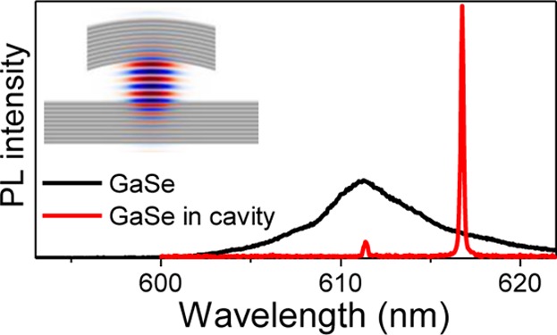
Integration of quasi-two-dimensional (2D) films of metal–chalcogenides in optical microcavities permits new photonic applications of these materials. Here we present tunable microcavities with monolayer MoS2 or few monolayer GaSe films. We observe significant modification of spectral and temporal properties of photoluminescence (PL): PL is emitted in spectrally narrow and wavelength-tunable cavity modes with quality factors up to 7400; a 10-fold PL lifetime shortening is achieved, a consequence of Purcell enhancement of the spontaneous emission rate.
Keywords: Molybdenum disulfide, gallium selenide, 2D materials, tunable microcavities, Purcell effect, photonics
The discovery and research into remarkable properties of graphene1 has sparked interest in two-dimensional (2D) metal chalcogenides (MCs).2−4 MCs are a large family of compounds that include layered van der Waals crystals. Among them are many semiconducting materials with a variety of band gap energies attractive for use in optoelectronics.2−8 For light-emitting applications, some of the layered materials such as for example molybdenum and tungsten dichalcogenides need to be thinned down to a single atomic unit cell (e.g., S–Mo–S for MoS2), as only in this form do they behave as direct band gap semiconductors.9−11 Layered III–VI crystals such as GaSe, InSe, and so forth are also attractive for 2D photonics as they exhibit direct band-gaps in films with a variety of thicknesses from a few to tens of nanometers,12,13 thus enabling flexibility in the device design. However, for materials of both types, use of thin films in photonic applications will require overcoming relatively low emission and absorption efficiency generally characteristic of thin layers of any semiconducting material.
One of the ways to enhance light absorption/emission in a semiconductor is to embed it in a microcavity (Fabry–Perot, photonic crystal, etc.)14−16 or a waveguide.17 So far, this has mainly been applied to graphene.18,19 Enhancement of photoluminescence (PL) in semiconducting MoS2 and WSe2 films coupled to photonic crystal cavities has also been demonstrated.20,21 More recently, strong exciton–photon coupling has been observed in a dielectric cavity containing synthesized MoS2 layers, emphasizing the dramatic effect optical cavities may have on the properties of thin films.22
Here we demonstrate tunable external cavity devices where thin films are deposited on a planar distributed Bragg reflector (DBR) and the cavity is completed by another DBR having a concave shape.23−26 We show that in this mirror configuration it is possible to form cavity modes confined in three dimensions and having mode volumes as low as 1.6 μm3 and quality factors, Q, up to 7400. This design allows tunability of the cavity size by adjusting the vertical displacement of the two mirrors and, therefore, allows spectral matching of the cavity mode wavelength with that of the emitter embedded in the device: we demonstrate wavelength tuning over 80 nm limited by the spectral width of the emitter only. We realize such devices for single atomic layers of molybdenum disulfide (MoS2) and few monolayer thick gallium selenide (GaSe) films and observe major modification of the emission spectra and strong peak PL intensity increase compared with the same films but with the top mirror moved out of the optical path. Using time-resolved PL spectroscopy, we directly observe the Purcell enhancement of the spontaneous emission rate for films placed in the cavity by measuring a 10-fold shortening of PL lifetimes in GaSe films. The enhancement of the radiative rate is further confirmed in continuous-wave (cw) PL: we observe clear PL saturation at high powers for a GaSe film on a flat DBR and no saturation for PL of the same film inside a cavity. By performing finite-difference time-domain (FDTD) calculations, we show that the observed PL intensity enhancement is also due to the highly directional cavity mode emission having narrow angular distribution and enabling improved light coupling to the collection optics.
Experimental Procedure
Figure 1a schematically shows a tunable microcavity formed by a planar bottom DBR and a top DBR having a concave shape.23−26 Both mirrors have reflectivity exceeding 99% for the design wavelength of 650 nm and a stop band of 200 nm as shown in Figure 1b. The calculated electric field distribution inside the cavity in Figure 1a shows confinement of the mode in both vertical and lateral directions (see Supporting Information). Arrays of concave mirrors with different nominal radii of curvature, Rc, from 5.6 to 25 μm are patterned using focused ion beam milling of a high flatness silica substrate (Supporting Information). Both the top and the bottom DBRs are fabricated by coating the substrates with 10 pairs of quarter-lambda SiO2/TiO2 layers.
Figure 1.
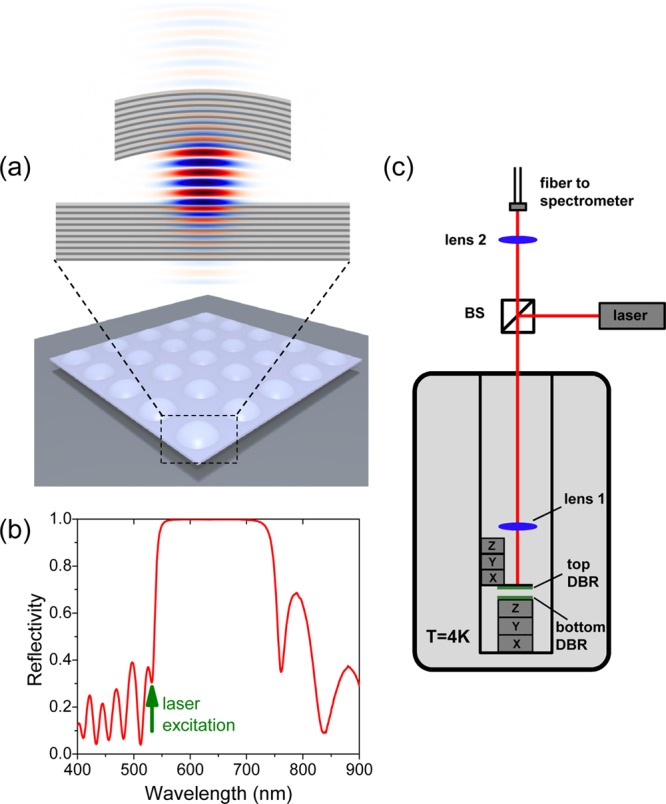
Microcavity design and schematic diagram of the experimental setup. (a) The microcavity is formed by a planar and a concave dielectric mirror having precisely controllable vertical displacement. Monolayer MoS2 and thin sheets of GaSe are transferred onto the flat mirror. The concave mirror provides the cavity mode confinement in three dimensions as shown in the calculated electric field distribution. (b) The reflectivity of the deposited DBR shows a wide stop-band in a range of ≈550–720 nm. The cw 532 nm laser excitation used for most of the measurements is shown with a vertical arrow and is spectrally just outside the stop-band. A transmission of 70% is observed for 532 nm. (c) Experimental setup showing the tunable open-access microcavity placed at T = 4.2 K inside a liquid helium cryostat.
Monolayer MoS2 and thin sheets of GaSe of thicknesses ranging from 30 to 100 nm have been obtained by mechanical cleavage of bulk crystals. GaSe films were deposited straight on the flat DBR substrate, whereas the MoS2 films were first deposited on a polymer and then transferred onto the flat DBR using standard transfer techniques.28 The thickness of the sheets was verified using atomic force microscopy.
Optical measurements were performed with the DBRs and samples placed at a temperature of 4.2 K. Both the flat and the concave DBR substrates were attached to XYZ nanopositioners. This permitted two types of PL experiments: (i) PL detection from the film on the flat DBR with the top DBR moved out of the optical path (the “half-cavity” configuration); (ii) PL from the films placed inside a full cavity, for which the top mirror was moved above the place on the film excited with the laser. Importantly, this experimental arrangement also permits control of the vertical cavity length, Lcav, enabling wavelength tuning of the cavity modes as described with the following expression:
| 1 |
Here, q, m, and n are longitudinal (q) and transverse (m, n) mode numbers for Hermite Gauss cavities. Lopt is the effective optical length of the cavity, which differs from the physical length Lcav due to penetration of the cavity mode into the DBRs. In our case, Lopt = Lcav + 1.25 μm, which is determined experimentally so that the mode wavelengths can be described with eq 1.
A laser diode at 532 nm and charge-coupled device were used for cw PL studies. For the time-resolved measurements a frequency-doubled pulsed titanium sapphire laser (at 415 nm) was used for excitation, and PL detection was carried out with a streak camera. The excitation laser was focused onto the sample with a lens having a focal length of 7.5 mm (lens 1 in Figure 1), resulting in a spot size on the film of 7 μm. The PL was collected by the same lens and was focused outside the cryostat by another lens (lens 2 in Figure 1) in a fiber delivering light to the detection system.
Results
Spectral Modification of PL by the Cavity
Figure 2 shows low-T PL spectra for MoS2 and GaSe films excited by a 532 nm cw laser. Broad spectra are obtained for the films in the “half-cavity” configuration. Here an excitation power density on the film of 6.5 kW/cm2 was used. The PL line width for both materials is determined by inhomogeneous broadening caused by variations of the exciton potential within the film area illuminated by the laser. In Figure 2a PL from a MoS2 monolayer is observed in a wide range from 640 to 740 nm (1.67–1.94 eV).9,29 Figure 2b shows PL for a 43 nm thick GaSe film with a spectrum in the range 600–625 nm (1.98–2.07 eV) corresponding to the emission from localized exciton states, probably occurring due to the interlayer stacking defects.30
Figure 2.
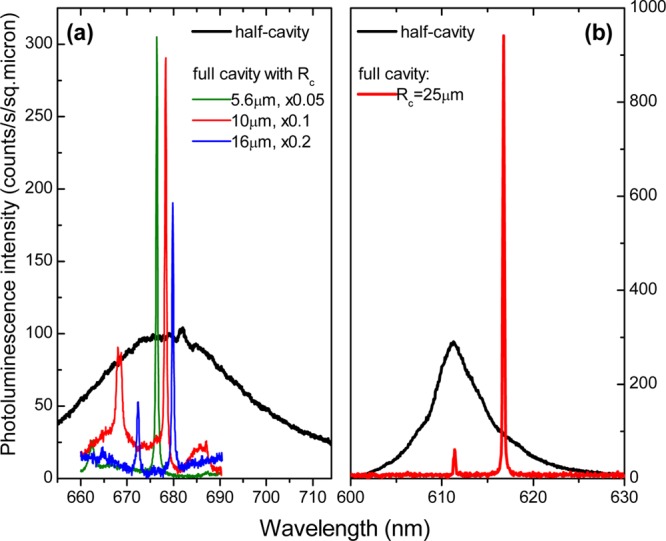
Thin film and cavity mode photoluminescence spectra. The broadband photoluminescence (PL) is collected from 2D films placed on the flat bottom DBR with the concave DBR moved out of the optical path. The narrow cavity modes are measured in PL when the microcavity is formed by placing the concave top mirror in the optical path. PL is measured at T = 4.2 K. (a) A PL spectrum of a monolayer MoS2 (black) is shown together with the cavity emission for the top mirror radii of curvature (Rc) of 5.6, 10, and 16 μm. Note the multiplication factors used for the cavity mode PL. (b) PL of GaSe 43 nm film and cavity PL in resonance with the low energy shoulder of the GaSe spectrum. Both in (a) and (b), the PL intensity is presented in counts per second per square micron of the emitter (see text for explanation of normalization procedure).
The cavity is formed by moving the top mirror above the optically excited area of the film, with the laser coupled through the top DBR (the “full-cavity” configuration). In this configuration the PL is coupled into cavity modes having typical Q-factors of a few 103 and for some mirrors reaching up to 7400 (Supporting Information). Although the laser spot is similar to the experiments with the half-cavities, the waist diameter of the longitudinal modes is ≈1 μm.25 Thus, in the case of the full cavity, PL is collected from a film area about 50 times smaller than in the case of a film placed on a planar DBR. This is accounted for in Figure 2 by using units of counts per second per square micron for PL intensity: the emission is assumed to originate from a spot with diameter of 1 and 7 μm for the “full-” and “half-cavity” configurations, respectively.
Figure 2 shows PL spectra observed for 2D film emission in a cavity for the same laser excitation density of 6.5 kW/cm2 incident on the film. The spectra with sharp peaks in Figure 2a show PL measured for a cavity with a MoS2 monolayer. The strongest peaks around 675–680 nm correspond to longitudinal modes described in eq 1 with m, n = 0. The green, red, and blue lines show spectra measured for different top mirrors with nominal radii of curvature, Rc, of 16, 10, and 5.6 μm, respectively. The measured Q-factors for the strongest modes in the spectra are 4000, 3000 and 1800, respectively. PL from modes with m, n ≠ 0 is also observed at shorter wavelengths.
For the full cavity having a concave DBR with Rc = 16, 10, and 5.6 μm, the intensity (in counts/s/μm2) at the wavelengths corresponding to the mode PL peaks is greater than the MoS2 monolayer PL by ≈10, 30, and 60 times, respectively. Note that for each experiment one of the longitudinal modes was tuned in resonance with MoS2 PL roughly at the same wavelength. For this, the vertical size of the cavity was adjusted to values varying for different Rc: PL measurements in Figure 2a were taken for Lcav ≈ 1.9 μm for the mirrors with Rc = 5.6 and 10 μm, and Lcav ≈ 2.9 μm for the mirror with Rc = 16 μm. PL enhancement by a factor of 10 is also observed for the GaSe film in Figure 2b. Here a cavity with Lcav ≈ 4.2 μm and a concave mirror with Rc = 25 μm was used, and a Q-factor of 3100 was observed.
By changing the distance between the two mirrors, and therefore the cavity length, the cavity resonance wavelength, λq,m,n, is tuned according to eq 1. In experiment, this is achieved by changing the voltage on the piezo element of the nanopositioner where the top DBR is attached. Figure 3 demonstrates the tuning for a cavity with a MoS2 monolayer. It is seen that the cavity modes can be tuned over a range of about 40 nm by gradually changing the cavity length. The bright peak marked in the plot corresponds to a fundamental longitudinal mode with q = 12 for the optical cavity length of around Lcav = 4.2 μm. Apart from this mode, several other transverse modes with m, n ≠ 0 are also visible. The emission of the MoS2 monolayer is centered at around 680 nm, and the intensity of the cavity modes is enhanced when they are tuned past this spectral window. Using a similar pair of mirrors, we were also able to tune the modes around the emission window of GaSe down to ≈600 nm. In general, the tuning is only limited by the size of the stop band, which is ≈200 nm in our case (see Figure 1b).
Figure 3.
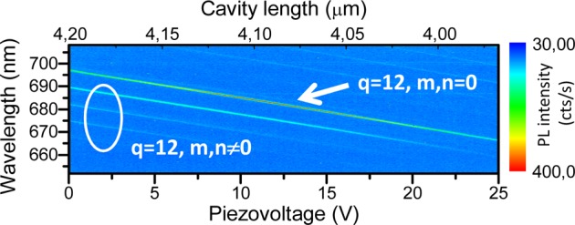
Tuning of the mode wavelength by adjusting the vertical length of the cavity. The distance between the DBRs is adjusted by changing the applied voltage on the piezo-nanopositioner. The figure shows a PL map obtained for such length tuning for the cavity containing a monolayer MoS2 film. PL of the modes is observed in a wide spectral range overlapping with the PL of the MoS2 film: the mode PL is enhanced when in resonance with MoS2 emission.
Temporal Modification of PL by a Cavity: Purcell Enhancement
The PL enhancement observed in Figure 2 can arise as a combined result of angular redistribution of light emission and enhancement of the spontaneous emission rate (Purcell enhancement). Here direct evidence for the Purcell enhancement is obtained from time-resolved PL measurements on GaSe films by comparing the radiative lifetimes with and without the effect of the cavity. Figure 4a shows PL decay curves for a 43 nm GaSe film excited at 415 nm with a pulsed laser. In both half- and full-cavity configurations the time-averaged excitation density was 2.6 kW/cm2. The cavity length is adjusted to Lcav ≈ 2.9 μm (an Rc = 10 μm cavity is used) so that a longitudinal cavity mode is coupled into the low energy shoulder of the GaSe emission at 613 nm as in Figure 2b. As seen in Figure 4a, without the effect of the cavity, PL decay with a lifetime of τhc ≈ 700 ps is observed, whereas in the full-cavity configuration the PL lifetime τfc ≈ 70 ps (both times are obtained using fitting with monoexponential decay functions). This measurement signifies the enhancement of the spontaneous emission rate in the tunable cavity device.
Figure 4.
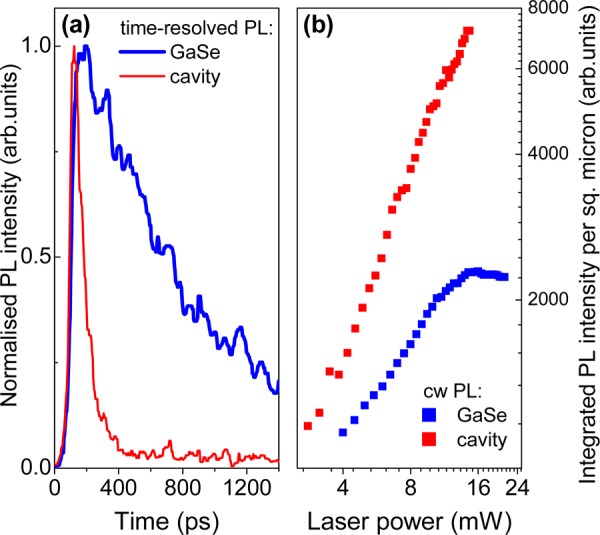
Observation of Purcell enhancement for GaSe thin film emission in a tunable microcavity. (a) PL traces under excitation with a pulsed laser at 415 nm, measured at T = 4.2 K using a streak-camera (spectral resolution of 0.2 nm). The traces are obtained by integrating the PL signal centered at 613 nm within the bandwidth of ≈2 nm in the spectrum measured by the streak-camera. The red curve shows the full-cavity PL decay, for which a lifetime of 70 ps is found. The blue trace shows PL decay with a lifetime of 700 ps in a film in the half-cavity configuration. (b) Photoluminescence power dependence for a GaSe film in a microcavity. PL measurements were performed at T = 4.2 K by varying the excitation power of a continuous-wave 532 nm laser. At high laser powers, a clear saturation of the GaSe film PL is observed (blue squares) when measured without the top concave mirror. In the full cavity, the cavity mode PL (red squares), fed by the GaSe film emission, shows no saturation. In the graph, the excitation power of the cavity mode is corrected by the measured transmission through the top mirror.
Figure 4b presents further evidence for the enhancement of the radiative recombination rate in a microcavity. Here we show PL power-dependences of the 43 nm thick GaSe film in the half- and full-cavity configurations measured with a 532 nm cw laser. For the full cavity we use the same Lcav and Rc as for the time-resolved experiments. The plot shows integrated PL intensity calculated under the full-cavity mode spectrum centered at 613 nm and having a fwhm of 0.15 nm (red squares), and under the same bandwidth of GaSe PL at the same center wavelength in the half-cavity case (blue squares). The reduced transmission of the green laser through the top DBR is taken into account, and the data are plotted as functions of the actual laser power incident on the GaSe film. In the case of the half-cavity configuration, a clear sublinear PL intensity growth with power is seen. PL saturation is observed at around P = 10 mW, indicating that the optical pumping rate exceeds the relatively low recombination rate 1/τhc (τhc ≈ 700 ps) of the localized exciton states in GaSe.30,31 In contrast to this, a much stronger PL increase with power is found for the cavity mode in the full-cavity configuration. No PL saturation is observed, indicating that the spontaneous recombination rate remains higher than the excitation rate in the whole range of powers used. This striking difference clearly indicates that the carrier radiative lifetime is markedly shorter in the case when the full cavity is formed,32 the effect quantified with the 10-fold PL decay time shortening in Figure 4a.
Calculation of the PL Enhancement in a Cavity
We start by estimating the PL enhancement due to increased directionality of the cavity mode toward the collection optics. For this the angular width of the fundamental cavity mode was calculated and compared with the radiation pattern for a dipole placed directly on the lower DBR but with no upper mirror using the FDTD technique33 (see Supporting Information for more details).
Figure 5 shows the simulated power radiated per unit solid angle in the far field for several mirror radii-of-curvature and separations as well as for the case without a top mirror. Only the upward flux is shown although the total flux radiated in all directions was calculated. We consider three cavities with parameters corresponding to the devices experimentally measured in Figure 2a: cavities C1, C2, and C3 are used having Rc of 16, 10, and 5.6 μm and Lcav of 2.98, 2.05, and 1.82 μm, respectively.
Figure 5.
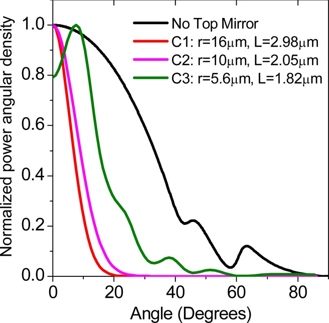
Calculated angular distribution of light emission from a 2D film with and without the cavity. The plot shows the normalized power angular density for the four cases: without the top mirror (the dipole placed on the flat DBR), and for the three different cavities, C1, C2, and C3 with the radii of curvature, Rc, and cavity length, Lcav, given on the graph.
In Figure 5, it is observed that in the case when no top mirror is present, the PL is emitted in a broad range of angles, whereas markedly more directional distributions are observed for the three cavities. We estimate that for the light to be collected by the objective placed above the microcavity (lens L1 in Figure 1c), light should be emitted within a 16.7° cone. We then obtain that in the case where no top mirror is present only 9% of the total power is collected through the objective. We find that for the cavities C1, C2, and C3, the fractions of power within ±16.7° are 47%, 44% and 20% respectively. The marked lowering for the cavity with the smallest Rc occurs because of scattering at the discontinuity between curved and planar regions of the top mirror (in the real cavity structures this discontinuity may be less sharp and its effect less pronounced). We thus find, that compared to the case when no top mirror is present, “geometrical” PL enhancements with factors Fg of 5.3, 4.9, and 2.2 occur in cavities C1, C2, and C3, respectively.
Further to the angular distribution, the FDTD method employed above can be used to calculate the Purcell enhancement factors, FP, using the calculated values for V and Q (Supporting Information). We obtain the following Purcell factors for the three considered cavities: FP1 = 41, FP2 = 59, and FP3 = 70. We also calculate the Purcell factor FP = 51 for the cavity used in the time-resolved measurements with Lcav ≈ 2.9 μm and Rc = 10 μm. These values for FP are for the emitter in perfect spatial and spectral overlap with the cavity mode. These values of FP provide an upper limit to the Purcell factor achievable in a cavity. In the experiment, we deal with an inhomogeneously broadened ensemble of spectrally narrow emitters distributed in a few μm diameter area of a 2D film. This means that spatial and spectral averaging of the Purcell enhancement will occur and a value of FP lower than given above is expected34 as discussed in the next subsection.
Discussion
First we note that the effect of nonradiative processes needs to be taken into account for the interpretation of the experimentally measured data and comparison with the theory. Using a simple approximation, we will take into account only three processes: optical pumping, a nonradiative decay with a time τnr, and a radiative decay with τr/FP (FP = 1 for a bare thin film and FP > 1 is expected for emitters in resonance with the cavity mode). The “state-filling” effects as observed in Figure 4b will be neglected. It is easy to show that the cw PL intensity IPL ∝ τnr/(τnr + τr/FP) and the characteristic PL decay time τPL = τnr(τr/FP)/(τnr + τr/FP).
In our work, direct evidence for the Purcell enhancement is obtained for the GaSe film in Figure 4. It can be shown that the ratio of ≈10 of the experimentally measured τPL values in the half- and full-cavity configurations corresponds to the lower limit for the Purcell enhancement factor (reached if τnr ≫ τr). The observation of the Purcell enhancement is itself an indirect evidence that τr is of the order or shorter than τnr for the localized excitons in GaSe.
In the case of MoS2 monolayer films τr/FP ≫ τnr9,35 for reasonable values of FP. (We measure PL decay times of ≈10 ps for MoS2 monolayer films in the half-cavity configuration.) In this case, nonradiative processes dominate, and the Purcell enhancement is not expected to be observable in time-resolved PL measurements. On the other hand, it is easy to show that in the absence of “state-filling” effects (as is the case for MoS229) and for τr/FP ≫ τnr, the cw PL intensity IPL ∝ FP in a cavity. Taking into account the geometrical enhancement due to the more directional cavity PL emission into the collection optics, IPL ∝ FPFg. By dividing the experimentally observed total PL enhancements of 10, 30, and 60, reported in Figure 2a, by the maximum expected Fg of ≈5, we obtain the lower limit for the PL enhancements caused purely by the Purcell effect. Thus, for Figure 2a the lower limits for FP from ≈2 to ≈12 are estimated.
For cavities investigated in both the time-resolved and cw measurements, the calculated maximum Purcell enhancements in the range of 41–70, as found in the previous subsection, exceed those observed in the experiment. One of the reasons for this discrepancy is the lowering of the measured Q-factors from their calculated values occurring as a result of cavity imperfections. In our work the calculated Q-factors are ≈2.5 times higher than the measured values. Furthermore, in order to reflect the finite in-plane size of the mode and varied coupling to the mode of independent emitters at different wavelengths, spatially and spectrally averaged Purcell enhancement should be calculated.34 In general the averaged Purcell factors are lower than the maximum values for the perfect spatial and spectral emitter-mode overlap. The averaging procedure requires the summation of IPL (in the case of cw PL enhancement) or of the simulated PL decay curves (in the case of lifetime shortening) over the emitters in the ensemble. The total PL or average characteristic PL decay time may then be determined. However, the result is sensitive to the ratio (τr/FP)/τnr since both τPL and IPL depend on these parameters. At this stage, insufficient information exists about the nonradiative decay processes in 2D films for such averaging to be carried out accurately.
Conclusions
In conclusion, we report on fabrication of tunable dielectric microcavities confining the photonic field in all three directions and comprising 2D films of metal–chalcogenides and show that the films’ spectral and temporal PL properties are strongly modified by the cavity. We observe strong cw PL enhancement for MoS2 and GaSe films placed inside the microcavity by up to a factor of 60 and directly measure the shortening of the PL lifetime in GaSe films by a factor of 10. Both cw and time-resolved observations provide evidence for the Purcell enhancement of the spontaneous emission rate in the studied cavities.
This work opens a route to a wide range of devices using 2D films and various van der Waals heterostructures as optically active materials. An advantage such devices would offer compared with traditional semiconductors is compatibility with a wide range of substrate materials including various dielectrics, polymers, and flexible substrates, permitting a wide choice of materials for fabrication of microcavities and waveguides.
Currently, the most advanced metal–chalcogenide heterostructures are built from exfoliated films, and the use of vertical cavity geometry in photonic applications is the most practical and advantageous, as the lateral device sizes are of the order 10–50 μm only. Use of other geometries such as waveguide, widely employed in semiconductor lasers and modulators, will only be applicable for synthetic films with sizes as large as a few hundreds of micron or larger.
Finally, we note that excitons in transition–metal dichalcogenides (MoS2, WS2, etc.) also exhibit large binding energies and high oscillator strength and are therefore promising for observation of room temperature polariton effects,22 opening a new field of devices utilizing highly nonlinear optical phenomena and cavity QED in a new material system of van der Waals crystals.
Acknowledgments
We thank the financial support of FP7 ITN S3NANO, ERC grant EXCIPOL 320570, the EPSRC Programme Grant EP/J007544/1, and Graphene Flagship grant 604391. A.A.P.T., M.S., D.N.K. and J.M.S. acknowledge support from the Leverhulme Trust. K.S.N. was supported by ERC and the Royal Society. F.W. was supported by the Royal Academy of Engineering. D.N.B. and N.N.K. acknowledge support by DPS RAS project II-5-B5.
Supporting Information Available
Additional details for the sample and device design and fabrication, further characterization data for the microcavities used in the experiments, and detailed account of the results of FDTD calculations of the optical modes in the external cavity devices used in our work. This material is available free of charge via the Internet at http://pubs.acs.org.
The authors declare no competing financial interest.
Supplementary Material
References
- Novoselov K. S.; Geim A. K.; Morozov S. V.; Jiang D.; Zhang Y.; Dubonos S. V.; Grigorieva I. V.; Firsov A. A. Science 2004, 306, 666. [DOI] [PubMed] [Google Scholar]
- Novoselov K. S.; Jiang D.; Schedin F.; Booth T. J.; Khotkevich V. V.; Morozov S. V.; Geim A. K. Proc. Natl. Acad. Sci. U.S.A. 2005, 102, 10451–10453. [DOI] [PMC free article] [PubMed] [Google Scholar]
- Wang Q. H.; Kalantar-Zadeh K.; Kis A.; Coleman J. N.; Strano M. S. Nat. Nanotechnol. 2012, 7, 699–712. [DOI] [PubMed] [Google Scholar]
- Xu X.; Yeo W.; Xiao D.; Heinz T. F. Nat. Phys. 2014, 10, 343. [Google Scholar]
- Radisavljevic D.; Radenovic A.; Brivio J.; Giacometti V.; Kis A. Nat. Nanotechnol. 2011, 6, 147. [DOI] [PubMed] [Google Scholar]
- Britnell L.; Ribeiro R. M.; Eckmann A.; Jalil R.; Belle B. D.; Mishchenko A.; Kim Y.-J.; Gorbachev R. V.; Georgiou T.; Morozov S. V.; Grigorenko A. N.; Geim A. K.; Casiraghi C.; Castro Neto A. H.; Novoselov K. S. Science 2013, 340, 1311. [DOI] [PubMed] [Google Scholar]
- Geim A. K.; Grigorieva I. V. Nature 2013, 499, 419. [DOI] [PubMed] [Google Scholar]
- Pospischil A.; Furchi M. M.; Mueller T. Nat. Nanotechnol. 2014, 9, 257. [DOI] [PubMed] [Google Scholar]
- Mak K.; Lee C.; Hone J.; Shan J.; Heinz T. Phys. Rev. Lett. 2010, 105, 136805. [DOI] [PubMed] [Google Scholar]
- Splendiani A.; Sun L.; Zhang Y.; Li T.; Kim J.; Chim C.-Y.; Galli G.; Wang F. Nano Lett. 2010, 10, 1271–1275. [DOI] [PubMed] [Google Scholar]
- Ross J. S.; Wu S.; Yu H.; Ghimire N. J.; Jones A. M.; Aivazian G.; Yan J.; Mandrus D. G.; Xiao D.; Yao W.; Xu X. Nat. Commun. 2013, 4, 1474. [DOI] [PubMed] [Google Scholar]
- Hu P.; Wen Z.; Wang L.; Tan P.; Xiao K. ACS Nano 2012, 6, 5988–5994. [DOI] [PubMed] [Google Scholar]
- Mudd G. W.; Svatek S. A.; Ren T.; Patan A.; Makarovsky O.; Eaves L.; Beton P. H.; Kovalyuk Z. D.; Lashkarev G. V.; Kudrynskyi Z. R.; Dmitriev A. I. Adv. Mater. 2013, 25, 5714–5718. [DOI] [PMC free article] [PubMed] [Google Scholar]
- Koyama F. J. Lightwave Technol. 2006, 24, 4502–4513. [Google Scholar]
- Hennessy K.; Badolato A.; Winger M.; Gerace D.; Atature M.; Gulde S.; Falt S.; Hu E. L.; Imamoglu A. Nature 2007, 445, 896. [DOI] [PubMed] [Google Scholar]
- Nowak A. K.; Portalupi S. L.; Giesz V.; Gazzano O.; Dal Savio C.; Braun P.-F.; Karrai K.; Arnold C.; Lanco L.; Sagnes I.; Lemaitre A.; Senellart P. Nat. Commun. 2014, 5, 3240. [DOI] [PMC free article] [PubMed] [Google Scholar]
- Holonyak N.; Kolbas R.; Dupuis R. D.; Dapkus P. D. IEEE J. Quantum Electron. 1980, 16, 170–186. [Google Scholar]
- Furchi M.; Urich A.; Pospischil A.; Lilley G.; Unterrainer K.; Detz H.; Klang P.; Andrews A. M.; Schrenk W.; Strasser G.; Mueller T. Nano Lett. 2012, 12, 2773–2777. [DOI] [PMC free article] [PubMed] [Google Scholar]
- Engel M.; Steiner M.; Lombardo A.; Ferrari A. C.; v. Lhneysen H.; Avouris P.; Krupke R. Nat. Commun. 2012, 3, 906. [DOI] [PMC free article] [PubMed] [Google Scholar]
- Gan X.; Gao Y.; Fai Mak K.; Yao X.; Shiue R.-J.; van der Zande A.; Trusheim M. E.; Hatami F.; Heinz T. F.; Hone J.; Englund D. Appl. Phys. Lett. 2013, 103, 181119. [DOI] [PMC free article] [PubMed] [Google Scholar]
- Wu S.; Buckley S.; Jones A. M.; Ross J. S.; Ghimire N. J.; Yan J.; Mandrus D. G.; Yao W.; Hatami F.; Vučković J.; Majumdar A.; Xu X. 2D Mater. 2014, 1, 011001. [Google Scholar]
- Liu X.; Galfsky T.; Sun Z.; Xia F.; Lin E.-C.; Lee Y. H.; Kna-Cohen S.; Menon V. M.. arXiv: 1406.4826 [physics.optics], 2014. [Google Scholar]
- Dolan P. R.; Hughes G. M.; Grazioso F.; Patton B. R.; Smith J. M. Opt. Lett. 2010, 35, 3556–8. [DOI] [PubMed] [Google Scholar]
- Barbour R. J.; Dalgarno P. A.; Curran A.; Nowak K. M.; Baker H. J.; Hall D. R.; Stoltz N. G.; Petroff P. M.; Warburton R. J. J. Appl. Phys. 2011, 110, 053107. [Google Scholar]
- Dufferwiel S.; Fras F.; Trichet A.; Walker P. M.; Li F.; Giriunas L.; Makhonin M. N.; Wilson L. R.; Smith J. M.; Clarke E.; Skolnick M. S.; Krizhanovskii D. N. Appl. Phys. Lett. 2014, 104, 192107. [Google Scholar]
- Greuter L.; Starosielec D.; Najer D.; Ludwig A.; Duempelmann L.; Rohner D.; Warburton R. J.. arXiv: 1408.1357 [cond-mat.mes-hall], 2014. [Google Scholar]
- Kretinin A. V.; et al. Nano Lett. 2014, 14, 3270–3276. [DOI] [PubMed] [Google Scholar]
- Sercombe D.; Schwarz S.; Del Pozo-Zamudio O.; Liu F.; Robinson B. J.; Chekhovich E. A.; Tartakovskii I. I.; Kolosov O.; Tartakovskii A. I. Sci. Rep. 2013, 3, 3489. [DOI] [PMC free article] [PubMed] [Google Scholar]
- Capozzi V.; Maschke K. Phys. Rev. B 1986, 34, 3924–3931. [DOI] [PubMed] [Google Scholar]
- Taylor R. A.; Rayn J. F. J. Phys. C: Solid State Phys. 1987, 20, 6175. [Google Scholar]
- Happ T. D.; Tartakovskii I. I.; Kulakovskii V. D.; Reithmaier J.-P.; Kamp M.; Forchel A. Phys. Rev. B 2002, 66, 041303. [Google Scholar]
- Oskooi A. F.; Roundy D.; Ibanescu M.; Bermel P.; Joannopoulos D. J.; Johnson S. G. Comput. Phys. Commun. 2010, 181, 687–702. [Google Scholar]
- Gérard J. M.; Sermage B.; Gayral B.; Legrand B.; Costard E.; Thierry-Mieg V. Phys. Rev. Lett. 1998, 81, 1110–1113. [Google Scholar]
- Xu X. Private communication.
Associated Data
This section collects any data citations, data availability statements, or supplementary materials included in this article.


