

Abstract
Purpose:
Active matrix flat panel imagers (AMFPI) have limited performance in low dose applications due to the electronic noise of the thin film transistor (TFT) array. A uniform layer of avalanche amorphous selenium (a-Se) called high gain avalanche rushing photoconductor (HARP) allows for signal amplification prior to readout from the TFT array, largely eliminating the effects of the electronic noise. The authors report preliminary avalanche gain measurements from the first HARP structure developed for direct deposition onto a TFT array.
Methods:
The HARP structure is fabricated on a glass substrate in the form of p-i-n, i.e., the electron blocking layer (p) followed by an intrinsic (i) a-Se layer and finally the hole blocking layer (n). All deposition procedures are scalable to large area detectors. Integrated charge is measured from pulsed optical excitation incident on the top electrode (as would in an indirect AMFPI) under continuous high voltage bias. Avalanche gain measurements were obtained from samples fabricated simultaneously at different locations in the evaporator to evaluate performance uniformity across large area.
Results:
An avalanche gain of up to 80 was obtained, which showed field dependence consistent with previous measurements from n-i-p HARP structures established for vacuum tubes. Measurements from multiple samples demonstrate the spatial uniformity of performance using large area deposition methods. Finally, the results were highly reproducible during the time course of the entire study.
Conclusions:
We present promising avalanche gain measurement results from a novel HARP structure that can be deposited onto a TFT array. This is a crucial step toward the practical feasibility of AMFPI with avalanche gain, enabling quantum noise limited performance down to a single x-ray photon per pixel.
Keywords: amorphous selenium, avalanche gain, flat panel imager, solid-state
1. INTRODUCTION
1.A. Importance of flat panel imager (FPI) with avalanche gain
Active matrix flat panel imagers (AMFPI) are replacing screen film and computed radiography because of their instantaneous readout and superior image quality. However, at low doses, AMFPI have limited performance due to the degradation effect of electronic noise in the thin film transistor (TFT) array readout.1 To overcome this limitation, either the electronic noise must be reduced or the signal amplified in the photoconductor prior to storage in the pixel capacitor and subsequent readout. We propose to use a uniform layer of amorphous selenium (a-Se), known as high gain avalanche rushing photoconductor (HARP) to amplify photogenerated charge prior to readout in the TFT array.2
Two of the proposed detectors3 which utilize solid-state avalanche a-Se are shown in Fig. 1, to produce x-ray quantum noise limited performance down to one x-ray photon per pixel. The indirect detection method [Fig. 1(a)], which is called SHARP-AMFPI, uses a thin HARP layer (e.g., 15 μm) to detect the optical photons generated from a high resolution x-ray scintillator and amplify the signal.2,4,5 The direct detection method [Fig. 1(b)], which is called field shaping multi-well avalanche detector (SWAD),6 creates a separate avalanche region inside the wells while maintaining nonavalanche fields in the bulk, where the majority of x-ray interactions occur.7,8 This removes the depth dependence in the avalanche gain9 and reduces the field at the electrode contacts to minimize dark current due to injection of charge carriers. The goal of this work is to develop large area HARP that can benefit both AMFPI concepts.
FIG. 1.
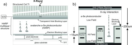
Two concepts of AMFPI with avalanche gain: (a) Indirect detection method which incorporates a structured scintillator with avalanche gain throughout the entire layer of a-Se. (b) Direct detection method which incorporates a thick absorption layer of a-Se and a separate avalanche region inside the wells above pixel electrodes.
1.B. Existing a-Se sensor technology
HARP structures consist of an intrinsic (i) layer of a-Se sandwiched between a hole blocking (n-type) and an electron blocking (p-type) layer to prevent charge injection from the positive and negative bias electrodes, respectively. These blocking layers are crucial for minimizing dark current while allowing the photogenerated charge to exit the a-Se. The existing HARP structure is fabricated in an n-i-p deposition sequence onto a transparent substrate (for light entrance) coated with indium tin oxide (ITO), which acts as the positive high voltage (HV) electrode. This structure has been used in HARP tubes,10,11 a hybrid-CMOS sensor through indium bump-bonding of HARP (Ref. 12) and electroded HARP.13 The largest HARP used in existing devices is 1 in. in diameter. On the other hand, large area a-Se direct conversion AMFPI have been used routinely for medical imaging for over a decade14–18 with well-established reliability and uniformity; however, they operate at ∼10 V/μm,15 while avalanche gain requires fields greater than 70 V/μm.19
1.C. Large area HARP for medical imaging
Both SHARP-AMFPI and SWAD requires a p-i-n deposition sequence of HARP. The main challenges are two-fold: the low temperature deposition of an n-layer to prevent the formation of polycrystalline aggregates in a-Se (which occurs at >50 °C)20 and the spatial uniformity of avalanche gain for large area medical image sensors. In addition, the n-layer needs to be transparent for indirect type sensors. The hole blocking layer in existing HARP requires high temperature deposition (220 °C) to achieve low dark current.21 Recently, various n-type organic polymers with low temperature deposition, e.g., C60 doped polymer and perylenetetracarboxylic bisbenzimidazole (PTCBI) have been used with direct con version a-Se but have not supported electric fields (ESe) greater than 45 V/μm.22,23
In this work, we present the first avalanche-gain measurements from a p-i-n HARP structure fabricated using deposition methods scalable to large area. Our promising results demonstrate the potential of combining the previous successes in small area HARP imaging tube in avalanche mode and large area direct AMFPI in nonavalanche mode, to develop AMFPI with programmable avalanche gain for medical imaging.
2. METHODS
2.A. Sample structure
We developed a p-i-n HARP structure shown in Fig. 2(a). The glass substrate is coated with ∼100 nm of chromium (Cr), which acts as the negative bias electrode. Then, a 2 μm thick p-layer is thermally deposited, which traps injected electrons while permitting hole transport. The i-layer, for optical sensing and avalanche multiplication, is stabilized a-Se with a thickness of 15 μm. A 2 μm thick, wide band gap, transparent organic polymer is then vacuum deposited, at room temperature, onto the i-layer to block hole injection. The top electrode is a semitransparent Cr layer ∼20 nm thick to allow for transmission of optical photons. The entire structure is encapsulated with a transparent organic insulator which was shown to improve the reliability of the device. For a clinical SHARP-AMFPI, a top electrode with high light transmission is required. Established room-temperature ITO sputtering technology can be utilized.24 Figure 2(b) shows one of the samples tested. There are four separate HV electrodes (sensors) to test gain uniformity across each sample. All samples were fabricated simultaneously in an experimental a-Se coater that was geometrically scaled down to mimic the properties of a commercial coater capable of producing AMFPI up to 17 in. × 17 in.
FIG. 2.

(a) Cross section schematic of the p-i-n HARP structure. (b) Top view of a HARP test structure. There are four Cr HV electrodes (sensors) per test structure.
2.B. Experimental procedures
Measurements were performed in a grounded, light tight metal box. The samples were exposed to 440 nm blue laser excitation pulses with a full width at half maximum (FWHM) of 40 ps. The common bottom electrode on the glass substrate was used to collect signal charge. The signal was read through a 1 GHz oscilloscope with a 1 MΩ input resistance to produce a charge integrating circuit with a sensitivity of 13 mV/pC. The top electrode was biased with positive high voltage, which was varied from 10 to 2260 V in 10 V increments. This corresponds to ESe of 0.5–105 V/μm. Each bias voltage was held for ∼5 s. Dark current remains low and is subtracted as an offset to obtain the signal due to photogenerated charge and avalanche gain. Between repeated measurements, the high voltage was removed and the sample was exposed to light pulses to remove any space charge at layer interfaces. The samples were tested over the course of one week.
3. RESULTS
3.A. Avalanche gain fitted to theory
Figure 3 shows the average integrated signal charge from the four sensors on one HARP structure as a function of ESe. A two-part empirical fitting has been performed using Origin 9.1 (OriginLab, Nothampton, MA). The measurement at ESe < 70 V/μm was fitted to the Onsager theory of photogenerated charge recombination.25 At ESe > 70 V/μm, the avalanche gain is fitted to the impact ionization model by Juška19
| (1) |
where D is the thickness of the a-Se and δIIC is the impact ionization parameter given by
| (2) |
FIG. 3.

Average gain measurements from one sample fitted to theory: measurements at ESe < 70 V/μm are fitted to the Onsager theory and the measurements at ESe > 70 V/μm are fitted to avalanche gain theory [Eq. (1)].
where β1 and β2 are fitting parameters. The fitted values for β1 and β2 are 4101 ± 400 μm −1 and 990 ± 100 V/μm, respectively. Published values for β1 range from 949 to 1700 μm −1 and values for β2 range from 849 to 930 V/μm.26,27 Variations in these fitting parameters often arise due to uncertainties in ESe, which are typically a result of variations in the a-Se thicknesses and blocking layers.28
3.B. Gain uniformity
Three samples with four sensors each were tested individually for gain. Figure 4 shows the gain measured from one sensor of each sample. The variation in gain between samples was under 10% at all applied fields. Eleven out of twelve sensors produced avalanche gain. Inspection of the failed sensor showed delamination of the encapsulation layer due to excessive tension to the HV cable and not a result of fabrication imperfections. There was no measurable degradation of the samples over the entire course of our study.
FIG. 4.

Uniformity of gain across the sensors from three different samples.
4. DISCUSSION
4.A. Improvements to the HARP structure
Due to poor electron transport in the hole blocking layer, a buildup of negative charge occurs at the interface between the hole-blocking layer and a-Se. While the low mobility could be used as a protection mechanism against permanent material breakdown,3,25 it needs to be optimized against memory effects. A large body of work in organic semiconductors has shown that doping polymer with electron transporting material can vary the electron mobility by several orders of magnitude and may help future efforts in optimizing the n-layer.29,30 The correct choice of polymers can also protect a-Se from recrystallization.31
4.B. Integration with a TFT array
While the hole blocking layer can be further optimized, our immediate plan is to deposit the new HARP structure onto a large area TFT array to better understand the spatial uniformity of gain and the additional challenges imposed by the TFT arrays. The TFT arrays used for AMFPI have surface variations on the micron scale from the lithography processes used in fabrication. We have previously developed planarization techniques to prepare it for HARP deposition.32 The most crucial step in future development of AMFPI with avalanche gain is the elimination of electric field hot spot (ESe > 120 V/μm) in HARP.6
5. CONCLUSION
We presented the first HARP structure with the potential to be placed on a TFT array for future development of large area AMFPI with avalanche gain. We have shown gain of 80 with good spatial uniformity and temporal repeatability. Our future work will continue to optimize the charge transport in the blocking layers and deposit the new HARP structure onto a TFT array to investigate avalanche gain with a pixelated readout.
ACKNOWLEDGMENTS
The authors gratefully acknowledge financial support from the National Institutes of Health (R01 EB002655 and R01 CA148053). Research on blocking layers was carried out in part at the Center for Functional Nanomaterials, Brookhaven National Laboratory, which is supported by the U.S. Department of Energy, Office of Basic Energy Sciences, under Contract No. DE-AC02-98CH10886.
REFERENCES
- 1.Koch A. et al. , “Detective quantum efficiency of an x-ray image intensifier chain as a benchmark for amorphous silicon flat panel detectors,” Proc. SPIE 4320, 115–120 (2001). 10.1117/12.430919 [DOI] [Google Scholar]
- 2.Wronski M. M. et al. , “A solid-state amorphous selenium avalanche technology for low photon flux imaging applications,” Med. Phys. 37, 4982–4985 (2010). 10.1118/1.3483096 [DOI] [PMC free article] [PubMed] [Google Scholar]
- 3.Goldan A. H. et al. , “Nanopattern multi-well avalanche selenium detector with picosecond time resolution,” in IEEE Nuclear Science Symposium and Medical Imaging Conference (IEEE NSS/MIC) (IEEE, Seattle, WA, 2013). [Google Scholar]
- 4.Zhao W. et al. , “Indirect flat-panel detector with avalanche gain: Design and operation of the avalanche photoconductor,” Proc. SPIE 5745, 352–360 (2005). 10.1117/12.597295 [DOI] [Google Scholar]
- 5.Wronski M. et al. , “Scintillator high-gain avalanche rushing photoconductor active-matrix flat panel imager: Zero-spatial frequency x-ray imaging properties of the solid-state SHARP sensor structure,” Med. Phys. 39, 7102–7109 (2012). 10.1118/1.4760989 [DOI] [PMC free article] [PubMed] [Google Scholar]
- 6.Goldan A. H. and Zhao W., “A field-shaping multi-well avalanche detector for direct conversion amorphous selenium,” Med. Phys. 40, 010702 (3pp.) (2013). 10.1118/1.4769110 [DOI] [PMC free article] [PubMed] [Google Scholar]
- 7.Goldan A. et al. , “Unipolar time-differential pulse response with a solid-state Charpak photoconductor,” Appl. Phys. Lett. 101, 213503 (2012). 10.1063/1.4766726 [DOI] [Google Scholar]
- 8.Goldan A. et al. , “Reduced photocurrent lag using unipolar solid-state photoconductive detector structures: Application to stabilized nip amorphous selenium,” Appl. Phys. Lett. 96, 053507 (2010). 10.1063/1.3302454 [DOI] [Google Scholar]
- 9.Hunt D., Tanioka K., and Rowlands J., “X-ray imaging using avalanche multiplication in amorphous selenium: Investigation of depth dependent avalanche noise,” Med. Phys. 34, 976–986 (2007). 10.1118/1.2437097 [DOI] [PubMed] [Google Scholar]
- 10.Tanioka K., “High-gain avalanche rushing amorphous photoconductor (HARP) detector,” Nucl. Instrum. Methods Phys. Res., Sect. A 608, S15–S17 (2009). 10.1016/j.nima.2009.05.066 [DOI] [Google Scholar]
- 11.Li D. and Zhao W., “SAPHIRE (scintillator avalanche photoconductor with high resolution emitter readout) for low dose x-ray imaging: Spatial resolution,” Med. Phys. 35, 3151–3161 (2008). 10.1118/1.2937652 [DOI] [PMC free article] [PubMed] [Google Scholar]
- 12.Takiguchi Y. et al. , “CMOS imager hybridized to an avalanche multiplied film,” IEEE Trans. Electron Devices 44, 1783–1788 (1997). 10.1109/16.628837 [DOI] [Google Scholar]
- 13.Bubon O. et al. , “Electroded avalanche amorphous selenium (a-Se) photosensor,” Curr. Appl. Phys. 12, 983–988 (2012). 10.1016/j.cap.2011.12.023 [DOI] [PMC free article] [PubMed] [Google Scholar]
- 14.Rowlands J. A. et al. , “Flat-panel digital radiology with amorphous selenium and active-matrix readout,” RadioGraphics 17, 753–760 (1997). 10.1148/radiographics.17.3.9153709 [DOI] [PubMed] [Google Scholar]
- 15.Zhao W. and Rowlands J., “X-ray imaging using amorphous selenium: Feasibility of a flat panel self-scanned detector for digital radiology,” Med. Phys. 22, 1595–1604 (1995). 10.1118/1.597628 [DOI] [PubMed] [Google Scholar]
- 16.Zhao W. et al. , “Imaging performance of amorphous selenium based flat-panel detectors for digital mammography: Characterization of a small area prototype detector,” Med. Phys. 30, 254–263 (2003). 10.1118/1.1538233 [DOI] [PubMed] [Google Scholar]
- 17.Hunt D., Tousignant O., and Rowlands J., “Evaluation of the imaging properties of an amorphous selenium-based flat panel detector for digital fluoroscopy,” Med. Phys. 31, 1166–1175 (2004). 10.1118/1.1707755 [DOI] [PubMed] [Google Scholar]
- 18.Bloomquist A. K. et al. , “Lag and ghosting in a clinical flat-panel selenium digital mammography system,” Med. Phys. 33, 2998–3005 (2006). 10.1118/1.2218315 [DOI] [PubMed] [Google Scholar]
- 19.Juška G. and Arlauskas K., “Impact ionization and mobilities of charge carriers at high electric fields in amorphous selenium,” Phys. Status Solidi A 59, 389–393 (1980). 10.1002/pssa.2210590151 [DOI] [Google Scholar]
- 20.Stephens R., “Relaxation effects in glassy selenium,” J. Non-Cryst. Solids 20, 75–81 (1976). 10.1016/0022-3093(76)90108-3 [DOI] [Google Scholar]
- 21.Kikuchi K. et al. , “Hole-blocking mechanism in high-gain avalanche rushing amorphous photoconductor (HARP) film,” Phys. Status Solidi C 8, 2800–2803 (2011). 10.1002/pssc.201084055 [DOI] [Google Scholar]
- 22.Abbaszadeh S. et al. , “Investigation of hole-blocking contacts for high-conversion-gain amorphous selenium detectors for x-ray imaging,” IEEE Trans. Electron Devices 59, 2403–2409 (2012). 10.1109/TED.2012.2204998 [DOI] [Google Scholar]
- 23.Abbaszadeh S., Allec N., and Karim K. S., “Improving amorphous selenium photodetector performance using an organic semiconductor,” Key Eng. Mater. 543, 451–454 (2013). 10.4028/www.scientific.net/kem.543.451 [DOI] [Google Scholar]
- 24.Gorjanc T. et al. , “Room temperature deposition of ITO using rf magnetron sputtering,” Thin Solid Films 413, 181–185 (2002). 10.1016/S0040-6090(02)00425-X [DOI] [Google Scholar]
- 25.Pai D. M. and Enck R. C., “Onsager mechanism of photogeneration in amorphous selenium,” Phys. Rev. B 11, 5163–5174 (1975). 10.1103/PhysRevB.11.5163 [DOI] [Google Scholar]
- 26.Tsuji K. et al. , “Avalanche phenomenon in amorphous selenium,” Optoelectronics-Devices and Technology 9, 367–378 (1994). [Google Scholar]
- 27.Hunt D. C., Kirby S. S., and Rowlands J. A., “X-ray imaging with amorphous selenium: X-ray to charge conversion gain and avalanche multiplication gain,” Med. Phys. 29, 2464–2471 (2002). 10.1118/1.1513157 [DOI] [PubMed] [Google Scholar]
- 28.Tanaka K., “Avalanche breakdown in amorphous selenium (a-Se) and related materials: Brief review, critique, and proposal,” J. Optoelectron. Adv. Mater. 16, 243–251 (2014). [Google Scholar]
- 29.Watano H. and Sato M., “Development of high-image quality and high-durbality direct conversion digital radiography system ‘FDR AcSelerate’,” Fujifilm Res. Dev. 55, 6–9 (2009). [Google Scholar]
- 30.Murti D. K. et al. , “Electron transport in a molecularly doped polymer,” J. Phys. D: Appl. Phys. 24, 953–957 (1991). 10.1088/0022-3727/24/6/021 [DOI] [Google Scholar]
- 31.Nariyuki F. et al. , “New development of large-area direct conversion detector for digital radiography using amorphous selenium with a C60-doped polymer layer,” Proc. SPIE 7622, 762240-1–762240-7 (2010). 10.1117/12.840788 [DOI] [Google Scholar]
- 32.Hsiao H. and Zhao W., “WE-A-201B-03: Resistive interface layer for Flat-Panel imager (FPI) with avalanche gain,” Med. Phys. 37, 3412–3413 (2010). 10.1118/1.3469335 [DOI] [Google Scholar]