

Abstract
Efficient selection of semiconducting single-walled carbon nanotubes (SWNTs) from as-grown nanotube samples is crucial for their application as printable and flexible semiconductors in field-effect transistors (FETs). In this study, we use atactic poly(9-dodecyl-9-methyl-fluorene) (a-PF-1-12), a polyfluorene derivative with asymmetric side-chains, for the selective dispersion of semiconducting SWNTs with large diameters (>1 nm) from plasma torch-grown SWNTs. Lowering the molecular weight of the dispersing polymer leads to a significant improvement of selectivity. Combining dense semiconducting SWNT networks deposited from an enriched SWNT dispersion with a polymer/metal-oxide hybrid dielectric enables transistors with balanced ambipolar, contact resistance-corrected mobilities of up to 50 cm2·V–1·s–1, low ohmic contact resistance, steep subthreshold swings (0.12–0.14 V/dec) and high on/off ratios (106) even for short channel lengths (<10 μm). These FETs operate at low voltages (<3 V) and show almost no current hysteresis. The resulting ambipolar complementary-like inverters exhibit gains up to 61.
Keywords: semiconducting single-walled carbon nanotubes, selective dispersion, polymer wrapping, ambipolar field-effect transistor, inverter
Introduction
Semiconducting single-walled carbon nanotubes (SWNTs) are attractive materials for application in logic circuits and optoelectronic devices1 such as field-effect transistors,2 inverters, ring oscillators,3 and light-emitting devices.4 They are processable from solution and are of great interest for stretchable and flexible electronics.5−8 Because all synthesis methods for SWNTs, such as chemical vapor deposition, laser ablation, or plasma torch growth, produce a mixture of metallic (m-SWNTs) and semiconducting SWNTs (s-SWNTs), various sorting methods have been developed over the years. Popular methods to enrich s-SWNTs or to obtain single-species dispersions are gel-permeation chromatography,9 density gradient ultracentrifugation,10 and selective dispersion with conjugated polymers.11−14 However, it remains difficult to achieve both high selectivity and high yield. The dispersion of SWNTs with conjugated polymers in organic solvents, in particular with polyfluorene derivatives, is in many ways the simplest and most promising method. Although the exact selection mechanism is still unclear, a few guidelines have been established. The number and type of side-chains attached to the polyfluorene backbone strongly influence the amount and diameter-range of the dispersed SWNTs. One alkyl-chain seems to be sufficient to selectively disperse s-SWNTs.15 Longer side-chains shift the range of wrapped s-SWNTs toward larger diameters and increase the yield.16 We previously showed that the molecular weight of the dispersing polyfluorene derivative and the viscosity of the organic solvent also have an impact on the selectivity, possibly due to modified reaggregation kinetics.17 Less viscous dispersion media (i.e., lower molecular weight of the dissolved polymer, lower viscosity of the solvent, or both) lead to higher selectivities but also to a lower yield. In particular, the choice of solvent can lead to very different selectivities for the same polymer.18 Toluene and xylenes were found to give the best selectivities for many polymers.
For the application of SWNT networks as active layers in field-effect transistors (FETs), only s-SWNTs are desired because m-SWNTs drastically increase the off-current of the channel. This is especially important for short channel devices (channel lengths, L < 10 μm) and dense SWNT films, which are necessary for high effective carrier mobilities and high drive-currents. High on/off ratios are achievable with low-density networks,19 but as soon as the network density increases, the on/off ratio drops as m-SWNTs start to form percolation paths. Even for long channels (100 μm), m-SWNTs (e.g., in unsorted SWNTs20) lead to increased off-currents when the SWNT density reaches values above 1 SWNT/μm. High carrier mobilities and high on/off ratios seem almost mutually exclusive for short channel devices due to residual m-SWNTs.
Another factor that may influence the on/off ratio of SWNT FETs is their ambipolar nature. For one-dimensional ambipolar semiconductors with transparent injection barriers the theoretically achievable on/off ratio decreases with the band gap.21 This is of particular importance for larger diameter s-SWNTs (>1 nm) with small bandgaps (<0.8 eV). Thus, large bandgap SWNTs would be preferable for maximum on/off ratios, but SWNTs with larger diameters (smaller bandgaps) also exhibit higher intrinsic mobilities and lower injection barriers.16,22−25
The ambipolar nature of SWNTs allows for the fabrication of complementary-like inverters, which consist of two transistors and are the central building block of logic circuits.3 Ambipolar inverters have the advantage of requiring only a single layer of semiconductor and can be used at positive and negative supply voltages. Low drive voltages, fast switching speeds, high gains, and large noise-margins are the most important parameters for inverters. All of them require transistors with high carrier mobilities, steep subthreshold swings, and negligible current hysteresis. To accomplish these properties with SWNT networks, unwanted trap states have to be minimized. These are often associated with water at the dielectric surface and defects created during the deposition of the dielectric.26,27 Back-gated devices with SiO2 as the dielectric, which are widely used for SWNT network transistors, often suffer from hysteresis19 unless they are encapsulated, for example, with a hydrophobic polymer.28 Low drive voltages, which are essential for practical application can be achieved by high capacitance dielectrics, such as ionogels,3 thin metal-oxide layers,22 (e.g., aluminum oxide or hafnium oxide) or self-assembled molecular dielectrics.29 In summary, in order to realize reproducible, high-performance SWNT network transistors and circuits, both nanotube selection as well as device structure and processing must be optimized.
Here, we use a polyfluorene derivative with asymmetric side chains (atactic poly(9-dodecyl-9-methyl-fluorene, a-PF-1-12) to disperse large diameter s-SWNTs with high yield and high selectivity. We demonstrate that lower molecular weights significantly improve the selectivity. Dense network transistors fabricated from those enriched s-SWNT dispersions with a polymer/metal oxide hybrid dielectric in top-gate geometry operate at low voltages with excellent on/off ratios and negligible hysteresis. They exhibit high and balanced ambipolar mobilities and can thus be applied in complementary-like inverters with high gains. We also demonstrate the detrimental impact of residual metallic SWNTs on device performance depending on channel length.
Experimental Section
Synthesis of Polymers
Three different molecular weights of atactic poly(9-dodecyl-9-methyl-fluorene) (a-PF-1-12, Figure 1b) were synthesized according to previously established protocols.30,31 Briefly, the lowest molecular weight (Mn = 8.5 kg·mol–1, Mw = 13.0 kg·mol–1, PDI = 1.54) was obtained from a Suzuki-type aryl–aryl cross coupling of /rac/-(2-bromo-9-dodecyl-9-methylfluorene)-7-(4,4,5,5-tetramethyl-1,3,2-dioxaborolane). The medium (Mn = 65.6 kg·mol–1, Mw = 128.0 kg·mol–1, PDI = 1.94) and high molecular weights (Mn = 391.0 kg·mol–1, Mw = 772.0 kg·mol–1, PDI = 1.97) were synthesized via a Yamamoto-type aryl–aryl coupling of the corresponding dibromo-monomer (2,7-dibromo-9-dodecyl-9-methylfluorene). All polymers were purified by solvent extraction with methanol, acetone, ethyl acetate, and chloroform. The molecular structure was confirmed by 1H NMR and 13C NMR, and the molar mass distributions were determined by gel permeation chromatography versus narrowly distributed polystyrene (PS) standards (Supporting Information, S1).
Figure 1.
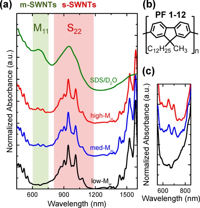
(a) Normalized absorbance spectra of plasma torch-grown SWNTs dispersed in SDS/D2O and a-PF-1-12/toluene with different molecular weights. (b) Molecular structure of a-PF-1-12. (c) Magnification of M11 region of the absorbance spectra.
Preparation of SWNT Dispersions
Single-walled carbon nanotubes (NanoIntegris, Inc., RN-220, plasma torch SWNTs, diameter 0.9–1.9 nm, SWNT content 60–70%, approximately 70% semiconducting SWNTs) were dispersed in a a-PF-1-12/toluene solution (2 mg·mL–1) at a concentration of 1.5 mg·mL–1 by bath ultrasonication for 75 min. To remove agglomerates and other residues (catalyst particles, amorphous carbon, etc.), we centrifuged the dispersions at 60 000 g (Beckman Coulter Avanti J26XP) and 268 000 g (Beckman Coulter OptimaMax XP table-top using polyallomer centrifuge tubes) for 1 h each. To reduce the amount of excess polymer in the dispersion, the SWNTs were pelletized by ultracentrifugation of the supernatant at 268,000 g for 14 h. The polymer solution was discarded. The pellet was washed several times with toluene and finally redispersed in toluene by bath sonication. Reference samples were obtained by dispersion of 1.5 mg·mL–1 of SWNTs (Super Purified Plasma SWNTs, Nanointegris, Inc.) in a 14 mg·mL–1 sodiumdodecylsulfate (SDS)/D2O solution.
Device Fabrication
Source-drain electrodes were patterned on glass substrates (Schott AF32 Eco) by photolithography (double-layer photoresist LOR5B/S1813) followed by electron-beam evaporation of 2 nm of chromium and 30 nm of gold, and lift-off with N-methyl-pyrrolidone. Channel lengths, L, (and widths, W) were 5, 10, 20 (10 000), and 40 μm (5000 μm) for field effect transistors and 5 (5 000) and 20 μm (20 000 μm) for inverter structures. SWNT thin films were deposited by spin-coating enriched SWNT dispersions with an absorbance of about 0.7 at 942 nm (1 cm cuvette). The SWNT thin films were annealed at 80 °C for a few minutes after each of the four coating steps and then rinsed with tetrahydrofuran and isopropanol to remove residual polymer. For inverter structures, the SWNT films were patterned by photolithography and oxygen plasma to reduce cross-talk between the transistors. SWNT films were annealed at 290 °C in dry nitrogen for 30 min to remove water and oxygen before applying a 10 nm thick poly(methyl methacrylate) layer (PMMA, Polymer Source, Inc., Mw = 315 kg·mol–1, PDI = 1.05) by spin-casting a 6 mg·mL–1 PMMA/n-butylacetate solution. Subsequently, a 50 nm thick HfO2 layer was deposited by atomic layer deposition (ALD, Ultratech Savannah 100). Tetrakis(dimethylamino) hafnium (TDMAH) was used as the hafnium precursor and water as the oxygen source at 100 °C. Finally, thermal shadow mask evaporation of 35 nm of silver as top gate electrodes completed the devices.
Characterization
SWNT dispersions were characterized by absorption spectroscopy using a Varian Cary 6000i UV–vis−NIR absorption spectrometer. The morphology of the SWNT thin films was determined by tapping-mode atomic force microscopy (AFM, Veeco Dimension V) and scanning electron microscopy (SEM, Carl Zeiss AURIGA at 1 kV operating voltage). Current–voltage characteristics of the transistors were recorded with an Agilent 4156C semiconductor parameter analyzer.
Results and Discussion
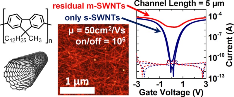
SWNT dispersions with different molecular weights of a-PF-1-12 (low-Mw = 13 kg·mol–1, med-Mw = 128 kg·mol–1, and high-Mw = 772 kg·mol–1) were prepared as described above, and their selectivity was determined by absorption spectroscopy. Figure 1 shows normalized absorption spectra including an SDS/D2O dispersion as a reference for unsorted SWNTs. Similar to dispersions with poly(9,9-di-n-dodecylfluorene-2,7-diyl)16,24 a strong selectivity toward semiconducting SWNTs with large diameters is found. In addition, the absorption peaks in the M11 region (600–750 nm) reveal that the relative amount of m-SWNTs strongly increases with the molecular weight of the dispersing polymer (Figure 1c). This trend corroborates our previous findings for other polyfluorene derivatives that dispersion selectivity increases with decreasing molecular weight.17 We assume that by increasing the molecular weight (i.e., increasing the viscosity of the polymer solution), the diffusion constant of the SWNTs decreases. Thus, metastable SWNT-polymer hybrids (i.e., m-SWNT) are kinetically stabilized in high-Mw dispersions, while they quickly reaggregate in low-Mw dispersions during the selection process. This again highlights the importance of knowing and reporting the molecular weight of the dispersing polymer. With respect to processing, this molecular weight dependence is advantageous. Low molecular weight polymers are easier to synthesize, often commercially available, they readily dissolve in organic solvents, and the SWNT-polymer dispersions are also less likely to form gels, which is a common processing problem. Although an exact quantification is difficult due to background absorption, it is clear that dispersions with low-Mw polymer contain an almost negligible amount of m-SWNTs. We thus expect transistors based on these dispersions to outperform those based on dispersions that still contain small amounts of metallic nanotubes (i.e., medium-Mw and high-Mw a-PF-1-12). In particular, residual m-SWNTs should have a strong impact on the on/off ratios of dense network transistors with short channel lengths. Thus, the selectivity of the dispersions can be further verified by transistor measurements.
The geometry of the fabricated top-gate/bottom-contact transistors and an SEM image of the dense random nanotube network are shown in Figure 2a,b. The linear density of the SWNT networks was approximately 15 SWNTs/μm (Supporting Information, S2), which is ideal for high effective mobilities and drive-currents. However, it is also high enough for the formation of percolation paths of m-SWNTs in short-channel devices (L < 10 μm), which would lead to high off-state conductivity. These network densities are uniform across the whole FET channel and reproducible for all fabricated samples. Raman spectra of the SWNT network reveal low intrinsic defect density and indicate no strong interaction between the SWNTs and the substrate that could influence the trap density within the film (Supporting Information, S3). Figure 2c shows the transfer characteristics in the linear regime (drain voltage VD = −10 mV) for transistors with different channel lengths based on a low-Mw dispersion. They show perfectly balanced ambipolar transport with turn-on voltages (VON) of −0.14 ± 0.04 V for holes and 0.16 ± 0.03 V for electrons. The transistors operate at very low gate voltages (VG) with subthreshold swings of 0.12 to 0.14 V/dec (Table 1) that are close to the theoretical limit (58.5 mV/dec at 295 K).32 These values confirm the absence of a significant number of trap states, as does the virtual absence of any current hysteresis, which is usually a major problem for SWNT transistors, in particular for ambipolar transistors. The gate leakage currents are very low and do not scale with the drain current. Clearly, the use of a hybrid dielectric of PMMA and HfO2 leads to excellent overall device characteristics. The interface between PMMA and the SWNT network results in a low trap density. The HfO2 layer enables low-voltage operation, low leakage currents, high breakthrough strength and provides natural encapsulation of the devices in a top-gate geometry. Device yield was nearly 100% with very little parameter spread. Only about 5% of the devices showed increased gate leakage, which was still orders of magnitude lower than the drain current.
Figure 2.
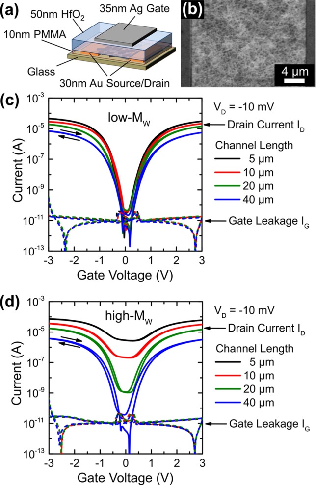
(a) Top-gate/bottom-contact transistor geometry with spin-coated SWNT network and PMMA/HfO2 hybrid dielectric. (b) SEM image of SWNT network within the channel. (c and d) Representative transfer characteristics of transistors with different channel lengths at VD = −10 mV with SWNT networks obtained from dispersions with low-Mw and high-Mw a-PF-1-12, respectively.
Table 1. Device Parameters of Transistors with SWNT Networks Obtained from Low-Mw Dispersions.
| VON (V) | μRC (cm2 V–1 s–1) | LOG(Ion/Ioff) | subthreshold swing (V/dec) | RCW (Ω·cm) | |
|---|---|---|---|---|---|
| electrons | 0.16 ± 0.03 | 49.6 | 5.6 ± 0.2 | 0.14 ± 0.01 | 313 |
| holes | –0.14 ± 0.04 | 49.6 | 5.8 ± 0.3 | 0.12 ± 0.01 | 205 |
μRC: Contact resistance-corrected mobility, RCW: Width-normalized contact resistance at VG = ± 3 V
For the operation of SWNT network transistors a high on/off ratio even for short channel lengths is most important and can serve as an indicator for the presence or absence of metallic nanotubes. As shown in Figure 2c the off-currents for transistors with SWNTs from low-Mw dispersions are close to the gate-leakage currents, while on-currents for VD = −10 mV reach tens of μA. For higher drain voltages, on-currents up to several mA are possible (see Supporting Information S4). Overall this leads to on/off current ratios of up to 106 (at VD = −10 mV). We would like to emphasize that these on/off ratios are conservative values compared to other reports. We extracted the off-currents from the low-current point for the reverse sweep, which was always above the gate leakage (Figure 2c). This method avoids artifacts such as transient “off”-currents that dip below the gate current and lead to inflated on/off ratios.
Ambipolar transistors are expected to have lower on/off ratios than unipolar transistors due to the overlap of hole and electron injection at higher drain voltages. To avoid this issue we applied very low drain voltages in all measurements, which also results in lower on-currents. A maximum on/off ratio of 107 can be reached for a transistor with L = 5 μm by increasing the drain voltage up to −300 mV (Supporting Information, S4). This value is quite high considering the theoretical limits for ambipolar transistors with a one-dimensional low-bandgap semiconductor as shown by Zhao et al.21 The maximum theoretical on/off ratios for single SWNTs with bandgaps of 0.6 and 0.8 eV are marked in Figure 3a. These bandgap values roughly represent the span of the S11 transitions and thus bandgaps of s-SWNTs sorted with a-PF-1-12. The theoretical on/off ratios are calculated for a single SWNT spanning the entire channel assuming transparent or low Schottky barriers. High Schottky barriers increase the on/off ratio substantially.21 As shown below, our SWNT transistors have ohmic contacts and the good on/off ratios cannot originate from Schottky barriers. Most likely, the presence of multiple nanotube–nanotube junctions in a network allows for lower off-currents. Nevertheless, the bandgap of the nanotubes used in network transistors should be considered when optimizing for on/off ratio. For high on/off ratios, smaller diameter SWNTs with larger bandgaps would be preferable. This is particularly important for transistors with very short channel lengths (<1 μm) and thus fewer nanotube junctions.
Figure 3.
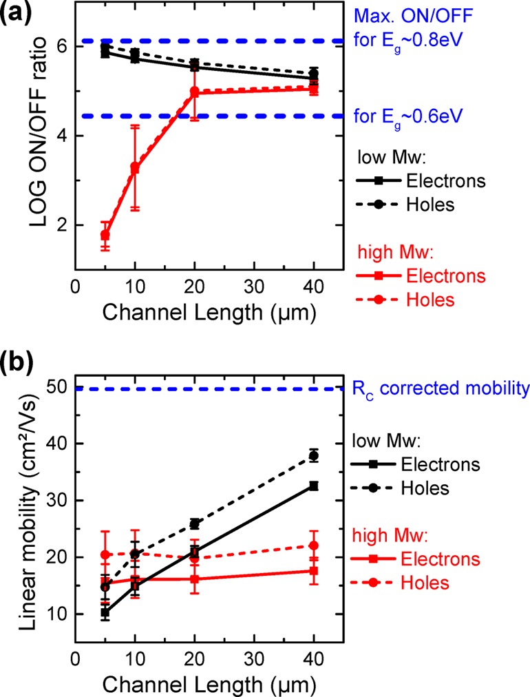
(a) On/off ratios and (b) field-effect mobilities as a function of channel length for network FETs based on SWNTs dispersed in low-Mw and high-Mw a-PF-1-12, respectively. Error bars indicate the standard deviations. Blue dashed lines indicate (a) the theoretical maximum on/off ratios for one-dimensional ambipolar semiconductors with a bandgap of 0.6 or 0.8 eV according to Zhao et al.21 and (b) the contact resistance-corrected mobility (for low-Mw dispersed SWNTs).
Further, the channel length has to be considered. Transistors with long channel lengths (>20 μm) can exhibit high on/off ratio even when metallic nanotubes are still present. This is shown in Figure 2d for transistors with SWNT networks based on high-Mw dispersions. For a channel length of 40 μm the on/off ratio is similar to that of devices based on low-Mw dispersions. Importantly though, this ratio drops dramatically as the channel length is reduced. In contrast to that, the on/off ratios for low-Mw dispersion transistors do not decrease but actually increase with shorter channel lengths. The negative impact of residual m-SWNTs is evident, as shown in Figure 3a. Overall, these data further corroborate the absorbance data. Networks deposited from the high-Mw dispersions contain a significant amount of residual m-SWNTs leading to an increased off-state conductance due to percolation paths of m-SWNTs. The number of such paths should follow a statistical distribution. This becomes evident in the standard deviations for the on/off ratios (indicated by the error bars in Figure 3a). While short and long channel devices show little spread in the on/off values, the numbers for L = 20 μm and L = 10 μm vary substantially. This suggests that the critical channel length for the formation of a significant number of metallic percolation paths in these devices lies between 5 and 10 μm.
For networks with many metallic nanotubes high on/off ratios and high mobilities are mutually exclusive, because high effective mobilities require very dense SWNT networks. We extracted the linear mobilities for holes and electrons for the presented transistors from the transconductance at VD = −10 mV (Supporting Information, S5). Due to the high capacitance of the hybrid dielectric high charge carrier densities can be accumulated within the SWNT thin film. Filling of the first sub-band of the SWNTs is found similar to observations by Shimotani et al. for electrolyte-gated networks.33 The maximum of the transconductance is used to calculate the field-effect mobility of the thin films. Since the electrostatic coupling of the SWNTs with the gate depends on the network density and because the quantum capacitance of the SWNTs cannot be neglected for high capacitance dielectrics, the effective capacitance for such networks differs from the simple plate–plate capacitance model.34 Using the plate–plate model overestimates the capacitance even for such dense networks. Instead, the intrinsic capacitance, which is calculated from the linear density of the SWNT network, should be used as the effective capacitance (Ceff, Supporting Information, S6). Based on the network density extracted from AFM and SEM images and measurements of the effective dielectric constant of the hybrid layer we obtain effective capacitance values between 66 and 84 nF·cm–2, which are substantially lower than values derived from the standard plate–plate capacitor model (0.110 and 0.145 μF·cm–2). For a conservative estimate of the mobilities we use an effective capacitance of 84 nF·cm–2 for all calculations. This way we obtain channel length-dependent charge carrier mobilities (Figure 3b) of 10.3–32.5 cm2·V–1·s–1 for electrons and 14.7–37.9 cm2·V–1·s–1 for holes for the low-Mw dispersed SWNTs. Using the simple plate–plate capacitance, the calculated mobility values are about 40% lower. This large difference clearly shows that the specific electrostatics of the nanotube network cannot be neglected even for dense networks when the gate dielectric is very thin. The standard deviation of the extracted mobilities varies from 10 to 15% for short channel devices (5 and 10 μm) to only 3% for longer channel lengths (20 and 40 μm) reflecting the high network uniformity and reproducibility.
The apparent channel length dependence of the mobility seems to originate from contact resistance at the source and drain electrodes and does not occur for SWNT films with residual m-SWNT (high-Mw-dispersion). A closer look at the contacts was required. The output characteristics for both holes and electrons (Figure 4a,b) reveal ohmic contacts and thus the contact resistance can be determined by applying the transmission line method.35 The total on-resistances for different channel lengths (RtotW, normalized for channel width) were extracted from the low-VD region of the output curves and extrapolated to zero channel length, which gives the total contact resistance (source + drain) RCW (Figure 4c). This method was originally developed to extract the contact resistance in thin film transistors but can also be applied to SWNT networks.5,36 The contact resistances in our devices are 313 Ω·cm and 205 Ω·cm for electrons and holes, respectively, when the channel is fully turned on, i.e. VG = ± 3 V (see Supporting Information, S7, for gate-voltage dependent contact resistance). These values are comparable to reports on SWNT network transistors with metal contacts (RCW ≈ 290–640 Ω·cm)36 but inferior to devices with metallic SWNTs as contacts (RCW < 5 Ω·cm).5 Given that the nanotubes only lie on top of the electrodes instead of the usually applied evaporation of metal onto the SWNTs, these contact resistance values are surprisingly low. The strong gate-field in a top-gate/bottom-contact geometry clearly improves the injection. This effect was also observed for organic thin film transistors.37,38 From the inverse slopes (m) of the linear RtotW versus L fits at different gate voltages (Figure 4d), the contact resistance-corrected charge carrier mobility (μRC) can be determined, using
as described by Natali et al.35 The corrected field-effect mobility for both holes and electrons is 49.6 cm2·V–1·s–1 (Figure 3b). The large difference between the contact resistance-corrected mobilities and those calculated from the transfer curves highlights the fact that for dense SWNT networks with high effective mobilities, contact resistance becomes the limiting factor, even when the contacts are ohmic. This information is especially important when down-scaling the channel length of network transistors and transistors with aligned SWNTs.39
Figure 4.
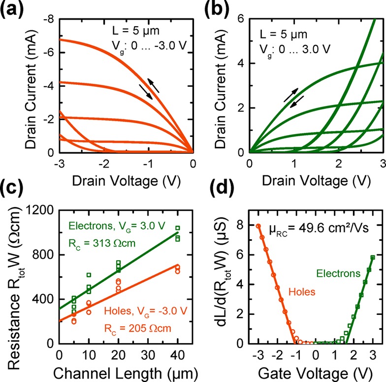
(a and b) Output characteristics of FETs fabricated with SWNTs dispersed in low-Mw a-PF-1-12 revealing good charge injection for both electrons and holes. (c) Width-normalized total resistance (channel + contact resistance) depending on channel length for contact resistance extraction at VG = −3 V and VG = 3 V, respectively. (d) Reciprocal slopes of the total resistance depending on gate voltage and resulting contact resistance-corrected mobility.
Overall, the demonstrated dense network transistors based on highly selective dispersions of s-SWNT with low-Mw a-PF-1-12 are in the high mobility and high on/off ratio region for short channel transistors based on solution processed random network SWNTs compared to previous reports.24,40 For further comparison with other SWNT-based devices, we refer to performance evaluations by Ding et al.24 and Derenskyi et al.19 These results also indicate that the transport through the SWNT network is strongly percolation limited compared to devices fabricated from unsorted SWNTs by dry deposition techniques with much larger average tube lengths.20 The carrier mobilities in networks of solution processed SWNTs are limited due to their average length (<2 μm)29 and the resulting percolation paths but show drastically improved on/off ratios for shorter channels.
Because these SWNT network transistors showed balanced ambipolar transport, they can be used to create complementary-like circuits. We built inverters with SWNTs from both low-Mw and high-Mw polymer dispersions that operated at low voltages (Figure 5). The inverters produced from low-Mw dispersions exhibit gains of up to 41 (5 μm channel) and 61 (20 μm channel) and excellent noise margins. The inverters operate in the first and third quadrant, that is, for both positive (not shown here) and negative supply voltages (VDD). Their trip voltage is close to VDD/2, which is expected for balanced ambipolar FETs. These inverters outperform similar ambipolar22 and hybrid41 devices based on SWNTs and are comparable to the best ambipolar polymer-based inverters.42,43 They show almost no hysteresis close to the trip point, which is essential to enable precise voltage inversion and large noise margins. However, they do not exhibit ideal rail-to-rail operation but reveal a Z-shape. This is a fundamental limitation when using ambipolar transistors with low threshold voltages. Due to the injection of opposite charge carriers at higher drain voltages (ambipolar regime; Supporting Information, S4) none of the transistors can ever be fully turned off. This leads to static power dissipation and a reduction of the output voltage for higher supply voltages.
Figure 5.
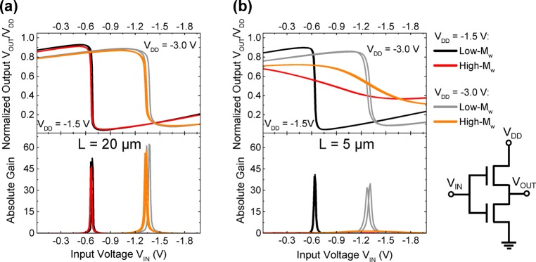
(Top) Normalized output voltages and (bottom) gains vs input voltage of ambipolar complementary-like inverters with channel lengths of (a) 20 μm and (b) 5 μm for SWNTs selected with low-Mw and high-Mw a-PF-1-12. (Inset) Inverter layout.
Inverters based on high-Mw dispersions show similar properties for long channels (L = 20 μm), in which the m-SWNTs have no noticeable impact on the switching behavior. However, for short channels (L = 5 μm), the m-SWNTs within the network cause increased off-currents leading to very low gains (<1.5) and loss of rail-to-rail operation. This again corroborates the detrimental impact of residual metallic nanotubes on the device performance of transistors with dense SWNT networks and short channel lengths, which are desired for high-speed circuits.
Conclusion
In summary, we showed that the selectivity of polymer dispersions strongly depends on the molecular weight of the polymer. With a low molecular weight, atactic poly(9-dodecyl-9-methyl-fluorene) proved most suitable for highly selective dispersions of semiconducting nanotubes with large diameters. By improving the selectivity, we were able to fabricate low-voltage network transistors with high contact resistance-corrected ambipolar carrier mobilities (50 cm2·V–1·s–1), excellent on/off ratios (106) even for short channel lengths (L < 10 μm) and negligible hysteresis. The transistors revealed perfectly ohmic contacts with low contact resistances (203 and 313 Ω·cm). Complementary-like inverters based on ambipolar SWNT transistors showed gains up to 61 and reasonable rail-to-rail operation. Our results demonstrate that highly selected, solution-processed s-SWNTs in optimized transistor structures lead to excellent device characteristics, which are not limited by residual m-SWNTs. However, scaling-down the channel length further in order to reduce the number of junctions within the SWNT network will be challenging as contact resistance becomes the performance limiting factor.
Acknowledgments
This research was funded by European Research Council under the European Union’s Seventh Framework Programme (FP/2007-2013)/ERC Grant Agreement No. 306298 (EN-LUMINATE). N.F., M.F., and U.S. acknowledge funding by the Deutsche Forschungsgemeinschaft (DFG)/FKZ SCHE 410/28-1. J.Z. thanks the Alfried Krupp von Bohlen und Halbach-Stiftung via the “Alfried Krupp Förderpreis für junge Hochschullehrer” and the Cluster of Excellence “Engineering of Advanced Materials” (EXC 315) for general support. The authors thank Udo Mundloch and the Institute of Advanced Materials and Processes (ZMP Fürth) for help with ultracentrifugation.
Supporting Information Available
GPC and NMR data for a-PF-1-12; AFM and SEM analysis of the SWNT thin films; Raman spectra of SWNT thin films; transfer curves at high source-drain bias and width-normalized on-currents and on-conductances; transconductance data; capacitance; and contact resistance calculations. This material is available free of charge via the Internet at http://pubs.acs.org.
The authors declare no competing financial interest.
Supplementary Material
References
- Jariwala D.; Sangwan V. K.; Lauhon L. J.; Marks T. J.; Hersam M. C. Carbon Nanomaterials for Electronics, Optoelectronics, Photovoltaics, and Sensing. Chem. Soc. Rev. 2013, 42, 2824–2860. [DOI] [PubMed] [Google Scholar]
- Sun D.; Timmermans M. Y.; Tian Y.; Nasibulin A. G.; Kauppinen E. I.; Kishimoto S.; Mizutani T.; Ohno Y. Flexible High-Performance Carbon Nanotube Integrated Circuits. Nat. Nanotechnol. 2011, 6, 156–161. [DOI] [PubMed] [Google Scholar]
- Ha M.; Seo J.-W. T.; Prabhumirashi P. L.; Zhang W.; Geier M. L.; Renn M. J.; Kim C. H.; Hersam M. C.; Frisbie C. D. Aerosol Jet Printed, Low Voltage, Electrolyte Gated Carbon Nanotube Ring Oscillators with Sub-5 μs Stage Delays. Nano Lett. 2013, 13, 954–960. [DOI] [PubMed] [Google Scholar]
- Jakubka F.; Backes C.; Gannott F.; Mundloch U.; Hauke F.; Hirsch A.; Zaumseil J. Mapping Charge Transport by Electroluminescence in Chirality-Selected Carbon Nanotube Networks. ACS Nano 2013, 7, 7428–7435. [DOI] [PubMed] [Google Scholar]
- Cao Q.; Hur S.-H.; Zhu Z.-T.; Sun Y. G.; Wang C.-J.; Meitl M. A.; Shim M.; Rogers J. A. Highly Bendable, Transparent Thin-Film Transistors That Use Carbon-Nanotube-based Conductors and Semiconductors with Elastomeric Dielectrics. Adv. Mater. 2006, 18, 304–309. [Google Scholar]
- Sun D.-M.; Liu C.; Ren W.-C.; Cheng H.-M. A Review of Carbon Nanotube- and Graphene-based Flexible Thin-Film Transistors. Small 2013, 9, 1188–1205. [DOI] [PubMed] [Google Scholar]
- Rouhi N.; Jain D.; Burke P. J. High-Performance Semiconducting Nanotube Inks: Progress and Prospects. ACS Nano 2011, 5, 8471–8487. [DOI] [PubMed] [Google Scholar]
- Xu F.; Wu M.-Y.; Safron N. S.; Roy S. S.; Jacobberger R. M.; Bindl D. J.; Seo J.-H.; Chang T.-H.; Ma Z.; Arnold M. S. Highly Stretchable Carbon Nanotube Transistors with Ion Gel Gate Dielectrics. Nano Lett. 2014, 14, 682–686. [DOI] [PubMed] [Google Scholar]
- Liu H.; Nishide D.; Tanaka T.; Kataura H. Large-scale Single-Chirality Separation of Single-Wall Carbon Nanotubes by Simple Gel Chromatography. Nat. Commun. 2011, 2, 309. [DOI] [PMC free article] [PubMed] [Google Scholar]
- Arnold M. S.; Green A. A.; Hulvat J. F.; Stupp S. I.; Hersam M. C. Sorting Carbon Nanotubes by Electronic Structure Using Density Differentiation. Nat. Nanotechnol. 2006, 1, 60–65. [DOI] [PubMed] [Google Scholar]
- Lemasson F.; Berton N.; Tittmann J.; Hennrich F.; Kappes M. M.; Mayor M. Polymer Library Comprising Fluorene and Carbazole Homo- and Copolymers for Selective Single-Walled Carbon Nanotubes Extraction. Macromolecules 2012, 45, 713–722. [Google Scholar]
- Gomulya W.; Gao J.; Loi M. A. Conjugated Polymer-Wrapped Carbon Nanotubes: Physical Properties and Device Applications. Eur. Phys. J. B 2013, 86, 404. [Google Scholar]
- Nish A.; Hwang J.-Y.; Doig J.; Nicholas R. J. Highly Selective Dispersion of Single-Walled Carbon Nanotubes Using Aromatic Polymers. Nat. Nanotechnol. 2007, 2, 640–646. [DOI] [PubMed] [Google Scholar]
- Liyanage L. S.; Lee H.; Patil N.; Park S.; Mitra S.; Bao Z.; Wong H.-S. P. Wafer-Scale Fabrication and Characterization of Thin-Film Transistors with Polythiophene-Sorted Semiconducting Carbon Nanotube Networks. ACS Nano 2012, 6, 451–458. [DOI] [PubMed] [Google Scholar]
- Fukumaru T.; Toshimitsu F.; Fujigaya T.; Nakashima N. Effects of the Chemical Structure of Polyfluorene on Selective Extraction of Semiconducting Single-Walled Carbon Nanotubes. Nanoscale 2014, 6, 5879–5886. [DOI] [PubMed] [Google Scholar]
- Gomulya W.; Costanzo G. D.; de Carvalho E. J. F.; Bisri S. Z.; Derenskyi V.; Fritsch M.; Fröhlich N.; Allard S.; Gordiichuk P.; Herrmann A.; Marrink S. J.; Dos Santos M. C.; Scherf U.; Loi M. A. Semiconducting Single-Walled Carbon Nanotubes on Demand by Polymer Wrapping. Adv. Mater. 2013, 25, 2948–2956. [DOI] [PubMed] [Google Scholar]
- Jakubka F.; Schießl S. P.; Martin S.; Englert J. M.; Hauke F.; Hirsch A.; Zaumseil J. Effect of Polymer Molecular Weight and Solution Parameters on Selective Dispersion of Single-Walled Carbon Nanotubes. ACS Macro Lett. 2012, 1, 815–819. [DOI] [PubMed] [Google Scholar]
- Hwang J.-Y.; Nish A.; Doig J.; Douven S.; Chen C.-W.; Chen L.-C.; Nicholas R. J. Polymer Structure and Solvent Effects on the Selective Dispersion of Single-Walled Carbon Nanotubes. J. Am. Chem. Soc. 2008, 130, 3543–3553. [DOI] [PubMed] [Google Scholar]
- Derenskyi V.; Gomulya W.; Rios J. M. S.; Fritsch M.; Fröhlich N.; Jung S.; Allard S.; Bisri S. Z.; Gordiichuk P.; Herrmann A.; Scherf U.; Loi M. A. Carbon Nanotube Network Ambipolar Field-Effect Transistors with 108 On/Off Ratio. Adv. Mater. 2014, 26, 5969–5975. [DOI] [PubMed] [Google Scholar]
- Sun D.-M.; Timmermans M. Y.; Kaskela A.; Nasibulin A. G.; Kishimoto S.; Mizutani T.; Kauppinen E. I.; Ohno Y. Mouldable All-Carbon Integrated Circuits. Nat. Commun. 2013, 4, 2302. [DOI] [PubMed] [Google Scholar]
- Zhao Y.; Candebat D.; Delker C.; Zi Y.; Janes D.; Appenzeller J.; Yang C. Understanding the Impact of Schottky Barriers on the Performance of Narrow Bandgap Nanowire Field Effect Transistors. Nano Lett. 2012, 12, 5331–5336. [DOI] [PubMed] [Google Scholar]
- Liu Z.; Zhao J.; Xu W.; Qian L.; Nie S.; Cui Z. Effect of Surface Wettability Properties on the Electrical Properties of Printed Carbon Nanotube Thin-Film Transistors on SiO2/Si Substrates. ACS Appl. Mater. Interfaces 2014, 6, 9997–10004. [DOI] [PubMed] [Google Scholar]
- Brady G. J.; Joo Y.; Singha Roy S.; Gopalan P.; Arnold M. S. High Performance Transistors via Aligned Polyfluorene-Sorted Carbon Nanotubes. Appl. Phys. Lett. 2014, 104, 083107. [Google Scholar]
- Ding J.; Li Z.; Lefebvre J.; Cheng F.; Dubey G.; Zou S.; Finnie P.; Hrdina A.; Scoles L.; Lopinski G. P.; Kingston C. T.; Simard B.; Malenfant P. R. L. Enrichment of Large-Diameter Semiconducting SWCNTs by Polyfluorene Extraction for High Network Density Thin Film Transistors. Nanoscale 2014, 6, 2328–2339. [DOI] [PubMed] [Google Scholar]
- Zhou X.; Park J.-Y.; Huang S.; Liu J.; McEuen P. Band Structure, Phonon Scattering, and the Performance Limit of Single-Walled Carbon Nanotube Transistors. Phys. Rev. Lett. 2005, 95, 146805. [DOI] [PubMed] [Google Scholar]
- Aguirre C. M.; Levesque P. L.; Paillet M.; Lapointe F.; St-Antoine B. C.; Desjardins P.; Martel R. The Role of the Oxygen/Water Redox Couple in Suppressing Electron Conduction in Field-Effect Transistors. Adv. Mater. 2009, 21, 3087–3091. [Google Scholar]
- Qian Q.; Li G.; Jin Y.; Liu J.; Zou Y.; Jiang K.; Fan S.; Li Q. Trap-State-Dominated Suppression of Electron Conduction in Carbon Nanotube Thin-Film Transistors. ACS Nano 2014, 8, 9597–9605. [DOI] [PubMed] [Google Scholar]
- Ha T.-J.; Kiriya D.; Chen K.; Javey A. Highly Stable Hysteresis-free Carbon Nanotube Thin-Film Transistors by Fluorocarbon Polymer Encapsulation. ACS Appl. Mater. Interfaces 2014, 6, 8441–8446. [DOI] [PubMed] [Google Scholar]
- Sangwan V. K.; Ortiz R. P.; Alaboson J. M. P.; Emery J. D.; Bedzyk M. J.; Lauhon L. J.; Marks T. J.; Hersam M. C. Fundamental Performance Limits of Carbon Nanotube Thin-Film Transistors Achieved Using Hybrid Molecular Dielectrics. ACS Nano 2012, 6, 7480–7488. [DOI] [PubMed] [Google Scholar]
- Kudla C. J.; Koenen N.; Pisula W.; Scherf U. First Synthesis of Isotactic Poly(9-alkyl1-9-alkyl2fluorene) via Directed Aryl–Aryl Coupling of Chiral AB-Type Monomers. Macromolecules 2009, 42, 3483–3488. [Google Scholar]
- Grell M.; Knoll W.; Lupo D.; Meisel A.; Miteva T.; Neher D.; Nothofer H.-G.; Scherf U.; Yasuda A. Blue Polarized Electroluminescence from a Liquid Crystalline Polyfluorene. Adv. Mater. 1999, 11, 671–675. [Google Scholar]
- Sze S. M.Physics of Semiconductor Devices; 2nd ed.; John Wiley & Sons: New York, 1981. [Google Scholar]
- Shimotani H.; Tsuda S.; Yuan H.; Yomogida Y.; Moriya R.; Takenobu T.; Yanagi K.; Iwasa Y. Continuous Band-Filling Control and One-Dimensional Transport in Metallic and Semiconducting Carbon Nanotube Tangled Films. Adv. Funct. Mater. 2014, 24, 3305–3311. [Google Scholar]
- Cao Q.; Xia M.; Kocabas C.; Shim M.; Rogers J. A.; Rotkin S. V. Gate Capacitance Coupling of Singled-Walled Carbon Nanotube Thin-Film Transistors. Appl. Phys. Lett. 2007, 90, 023516. [Google Scholar]
- Natali D.; Caironi M. Charge Injection in Solution-Processed Organic Field-Effect Transistors: Physics, Models, and Characterization Methods. Adv. Mater. 2012, 24, 1357–1387. [DOI] [PubMed] [Google Scholar]
- Jin S. H.; Shin J.; Cho I.-T.; Han S. Y.; Lee D. J.; Lee C. H.; Lee J.-H.; Rogers J. A. Solution-Processed Single-Walled Carbon Nanotube Field Effect Transistors and Bootstrapped Inverters for Disintegratable, Transient Electronics. Appl. Phys. Lett. 2014, 105, 013506. [Google Scholar]
- Gwinner M. C.; Jakubka F.; Gannott F.; Sirringhaus H.; Zaumseil J. Enhanced Ambipolar Charge Injection with Semiconducting Polymer/Carbon Nanotube Thin Films for Light-Emitting Transistors. ACS Nano 2012, 6, 539–548. [DOI] [PubMed] [Google Scholar]
- Richards T. J.; Sirringhaus H. Analysis of the Contact Resistance in Staggered, Top-Gate Organic Field-Effect Transistors. J. Appl. Phys. 2007, 102, 094510. [Google Scholar]
- Franklin A. D.; Farmer D. B.; Haensch W. Defining and Overcoming the Contact Resistance Challenge in Scaled Carbon Nanotube Transistors. ACS Nano 2014, 8, 7333–7339. [DOI] [PubMed] [Google Scholar]
- Wang H.; Mei J.; Liu P.; Schmidt K.; Jiménez-Osés G.; Osuna S.; Fang L.; Tassone C. J.; Zoombelt A. P.; Sokolov A. N.; Houk K. N.; Toney M. F.; Bao Z. Scalable and Selective Dispersion of Semiconducting Arc-Discharged Carbon Nanotubes by Dithiafulvalene/Thiophene Copolymers for Thin Film Transistors. ACS Nano 2013, 7, 2659–2668. [DOI] [PubMed] [Google Scholar]
- Kim B.; Jang S.; Geier M. L.; Prabhumirashi P. L.; Hersam M. C.; Dodabalapur A. Inkjet Printed Ambipolar Transistors and Inverters Based on Carbon Nanotube/Zinc Tin Oxide Heterostructures. Appl. Phys. Lett. 2014, 104, 062101. [Google Scholar]
- Fan J.; Yuen J. D.; Wang M.; Seifter J.; Seo J.-H.; Mohebbi A. R.; Zakhidov D.; Heeger A.; Wudl F. High-Performance Ambipolar Transistors and Inverters from an Ultralow Bandgap Polymer. Adv. Mater. 2012, 24, 2186–2190. [DOI] [PubMed] [Google Scholar]
- Chen Z.; Lemke H.; Albert-Seifried S.; Caironi M.; Nielsen M. M.; Heeney M.; Zhang W.; McCulloch I.; Sirringhaus H. High Mobility Ambipolar Charge Transport in Polyselenophene Conjugated Polymers. Adv. Mater. 2010, 22, 2371–2375. [DOI] [PubMed] [Google Scholar]
Associated Data
This section collects any data citations, data availability statements, or supplementary materials included in this article.