Abstract
We report on a vestibular prosthesis signal processor realized using an experimental field programmable analog array (FPAA). Completing signal processing functions in the analog domain, the processor is designed to help replace a malfunctioning inner ear sensory organ, a semicircular canal. Relying on angular head motion detected by an inertial sensor, the signal processor maps angular velocity into meaningful control signals to drive a current stimulator. To demonstrate biphasic pulse control a 1 kΩ resistive load was placed across an H-bridge circuit. When connected to a 2.4 V supply, a biphasic current of 100 μA was maintained at stimulation frequencies from 50–350 Hz, pulsewidths from 25–400 μsec, and interphase gaps ranging from 25–250 sec.
Keywords: Analog signal processing, biphasic stimulation, field programmable analog array (FPAA), vestibular prosthesis
I. Introduction
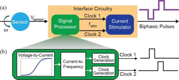
The vestibular system is responsible for establishing our sense of body orientation, maintaining balance, and stabilizing gaze [1]. Our natural peripheral vestibular system consists of three angular and two linear motion sensors located within the inner ear: the semi-circular canals (SCCs) and the otolith organs, respectively. The central nervous system (CNS) processes motion information sent by the peripheral sensors through the vestibular nerves. Defects in the sensors, vestibular nerves, or the CNS due to disease or injury cause problematic vestibular sensation [2]. Individuals suffering from loss of peripheral vestibular sensation could benefit greatly from a vestibular prosthesis. This device replaces the malfunctioning vestibular sensors with microfabricated sensors and stimulates the vestibular nerves with current pulses through interface circuitry and an implanted electrode array [3]. Similar to natural SCC neural coding for angular head rotation, the interface circuitry should encode the angular head velocity into a pulse rate [Fig. 1(a)]. A series of vestibular prostheses subsystems and prototypes have demonstrated promising results in overcoming peripheral vestibular loss in animal models [4]–[7]. Complementing these efforts is progress in low-power custom integrated interface circuitry [8]–[10], as well as integrating interface circuitry with the sensor [11].
Fig. 1.
Single canal vestibular prosthesis system diagram. (a) The interface circuitry consists of a signal processor and a current stimulator. (b) Circuit blocks constituting the signal processor. Operating in the analog domain, the voltage-to-current block encodes angular velocity as a drive current with a nonlinear transformation. The current-to-frequency block generates voltage pulses at a rate of fstim, the desired pulse rate. Two identical clock generation blocks produce digital control signals for a current stimulator to generate charge-balanced biphasic current pulses.
While promising, in-vivo studies indicate a pressing need for optimizing current stimulation paradigms as well as reducing spurious stimulation [12]. Thus, refining and optimizing encoding of angular velocity, and processing of angular velocity signals, is an essential step to achieving the clinical efficacy of a vestibular prosthesis. To investigate a potential platform for angular velocity encoding, this paper explores an experimental field programmable analog array (FPAA) development platform [13]. Accomplished completely in the analog domain, the signal processing circuitry generates a non-linear signal that codes angular velocity into a pulse rate for a single SCC [Fig. 1(b)]. Producing two out-of-phase clocks, the circuit can control all of the timing features of a biphasic pulse and ultimately drive a current stimulator for targeted activation of vestibular nerve fibers.
The rest of this paper is organized as follows. In Section II, we begin with a brief description of the FPAA and the procedure for realizing circuitry on the FPAA. In Section III, we provide the design specifications of the vestibular signal processor followed by a detailed description of the circuit blocks comprising the signal processor. Measurement and test results are discussed in Section IV. Finally, in Section V, we conclude by considering additional aspects of utilizing the FPAA platform such as scaling to a multichannel prosthesis and implementing alternative signal processing algorithms.
II. FPAA Architecture
The FPAA used is an experimental chip; the reconfigurable analog signal processor (RASP) 2.8 designed by the Integrated Computational Electronics Laboratory, Georgia Institute of Technology [13]. Although a commercial FPAA could also serve as a development platform [14], we chose the RASP 2.8 since its floating gate architecture provides greater functionality through the ability to program the switches with variable impedance. In addition, by operating the circuitry in weak inversion, considerable power saving can potentially be realized.
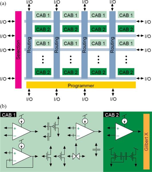
Fabricated with the Taiwan Semiconductor Manufacturing Company (TSMC) 0.35 μm 2P3M CMOS process and operating with a 2.4 V power supply, the RASP 2.8 is comprised of computational analog blocks (CABs) and an interconnect network (Fig. 2). A total of 32 CABs (CAB1 or CAB2) consist of circuit elements and blocks at different levels of complexity. Circuit elements/blocks such as transconductance amplifiers (OTAs), multi-input floating gates, nFET/pFET transistors, floating capacitors, Gilbert Multipliers, and floating-gate current mirrors are distributed among CAB1 and CAB2 [Fig. 2(b)]. The role of the interconnect network, which consists of switches (floating-gate pFETs) and interconnect lines, is to sensitize connections between CAB elements/blocks. In addition, global interconnect lines are also connected to input/output pins for voltage/current measurements.
Fig. 2.
Floating-gate FPAA architecture. (a) The FPAA consists of an 8 × 4 matrix of computational analog blocks (CABs) interconnected through crossbar networks. (b) CAB1 contains three operational transconductance amplifiers (OTAs), three floating capacitors (500 fF), two multi-input floating gates, a voltage buffer, a transmission gate, and nMOS/pMOS transistor arrays. CAB2 has two folded Gilbert multipliers and a floating gate current mirror, and a wide-linear-range OTA. I/O signals are routed to the rows and columns of the switch matrix [13].
To implement a particular circuit on the FPAA, connections are made by programming the necessary switches in the interconnect network. An automated placement and routing tool, the generic reconfigurable array specification and programming environment (GRASPER), determines which switches to activate. GRASPER converts a user-generated SPICE netlist describing the circuit into a netlist of switches [13]. To program a floating-gate pFET, negative charge is injected onto the floating-gate of the transistor. The amount of the charge trapped at the floating-gate affects the effective gate potential of the transistor and thus directly controls the conductance of the device. Briefly, the charge injection mechanism is accomplished by applying a high potential difference (~15 V) between the drain and the source terminals. As a result, a programming current, Iprog, passes across the two terminals. Iprog can be varied between 1 nA-32 μA, with higher causing more negative charge to be trapped at the floating-gate. The communication between the PC and the FPAA is achieved through a microprocessor-based board.
III. Signal Processor
For each SCC, the encoding of angular velocity into a pulse rate is based on a relationship validated in animal models [4]. This non-linear relationship between the angular velocity and the firing rate is represented as
| (1) |
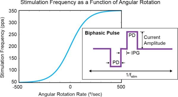
where ω is the angular velocity in °/sec, and is the pulse rate in pulses per second (pps). The offset value in the equation conveys a baseline pulse rate corresponding to zero angular velocity (Fig. 3).
Fig. 3.
Stimulation frequency, fstim, as a function of measured angular velocity [4]. The tanh function varies between 50–350 Hz with a baseline frequency of 200 Hz (zero angular head motion). A representative biphasic pulse is shown inside the graph. The amplitude and pulse duration (PD) of the cathodic pulse determine the charge delivered to the stimulation site. The PD and amplitude of the anodic pulse determine the charge returned from the tissue (balanced with input charge). The interphase gap (IPG) separates the two pulse periods and may be adjusted to optimize the neural response.
A biphasic current scheme [Fig. 3 (inset)] is generated to prevent any charge accumulation at the tissue site that can cause long-term adverse effects [15]. The amplitude and pulse duration (PD) of the cathodic pulse determines how much charge is delivered to the neural tissue. Similarly, the PD and the amplitude of the anodic pulse determine how much charge is returned from the tissue. The interphase gap (IPG) separates the two pulse periods to ensure the firing of the neuron. This control is essential for optimizing stimulus waveforms to reduce threshold, improve spatial selectivity and reduce spurious stimulation.
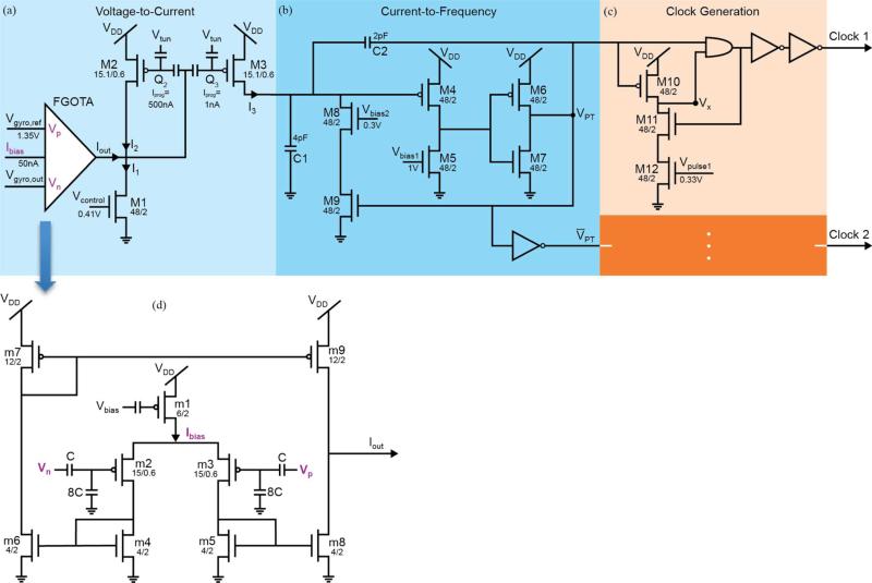
The signal processor provides the user with the freedom to control all timing features of a biphasic current pulse. The signal processor senses an analog voltage output from an inertial sensor, Vgyro,out , and converts this voltage into two out-of-phase clocks (Clock 1 and Clock 2) each with a frequency of fstim. In turn, Clock 1 and Clock 2 serve as control signals for a stimulator. The respective pulse duration of the two clocks determine the cathodic and the anodic PD of the biphasic current waveform. The phase difference between Clock 1 and Clock 2, less the PD, determines an IPG. The three blocks constituting the signal processor are the voltage-to-current converter block, the current-to-frequency converter block, and the clock generation block (Fig. 4). We describe each block in detail below.
Fig. 4.
Circuit schematic of the signal processor. The bias voltages Vgyro,ref, Vcontrol, Vbias1, Vbias2, Vpulse1 and Vpulse2 are generated using an off-chip DAC housed on a development board. (a) The voltage-to-current converter block transfers the voltage signal from the gyroscope, Vgyro,out, into a current signal, I3. The current I3 is related to angular velocity through a tanh function. The minimum level of I3 is controlled by Vcontrol. By adjusting Vgyro,ref an offset can be added to Vgyro,out. This serves to translate the I3 along the x-axis of the I3 versus Vgyro,out curve. (b) The current-to-frequency converter block converts the current signal, I3, into the pulse train output VPT. Linearly related to I3, the frequency of VPT determines fstim. (c) Two similar fully digital Clock Generation stages create Clock 1 and Clock 2. The pulse width of Clock 1 is controlled by Vpulse1 and a similar relationship exists for Clock 2. (d) The FGOTA is the core of the voltage-to-current converter block. In the sub-threshold region, the output current, Iout, of the FGOTA is related to its differential input voltage, Vp-Vn, through a tanh function Ibias. is the bias current which determines the region of operation and is set up during the programming stage by Vbias.
1) Voltage-to-Current Converter Block [Fig. 4(a), (d)]
The first block of the signal processor transfers the analog voltage output from an inertial sensor, gyroscope, into a current signal [Fig. 4(a)]. As indicated in (1), the stimulation frequency is related to angular velocity through a hyperbolic tangent function. In the spirit of biomorphic circuit design, we followed an integrate-and-fire neuron scheme utilizing a floating-gate OTA (FGOTA) [16]. In the sub-threshold region, the output current, Iout, of the FGOTA is related to its differential input voltage,Vp − Vn , through a tanh function
| (2) |
where κ is a constant relating the surface potential of a transistor to its gate voltage, α is the attenuation factor due to the capacitive divider at the input differential pair, Ibias is the bias current which determines the region of operation of the transistors, and UT is the thermal voltage. Thus, an FGOTA is at the core of the voltage-to-current converter block.
In our implementation, Vgyro,out, the output of the gyroscope, is connected to Vn input of the FGOTA. Vp is tied to Vgyro,out, the reference voltage for the gyroscope. To ensure that Iout is positive, M1, drawing I1 from the output node of the FGOTA, adds a DC offset. The current I1 is controlled by Vcontrol and I2 is the DC shifted version of −Iout. To ensure that I2 maintains fstim within the 50–350 Hz interval, I2 is scaled and mirrored using a mismatched current mirror circuit. The mirror circuit is formed by two floating-gate pFETs, M2 and M3, thereby creating I3. Since device sizes are fixed in the FPAA, the mismatch between M2 and M3 is controlled by programming varying amounts of charges (Q2 and Q3) onto their respective floating gates. For the Iprog values of M2 and M3 shown in Fig. 4, the I2/I3 ratio is measured to be ~80. The minimum level of I3 is controlled by Vcontrol. By adjusting Vgyro,ref an offset can be added to Vgyro,out. This serves to translate the I3 along the x-axis of the I3 versus Vgyro,out curve.
2) Current-to-Frequency Converter and Clock Generator Block [Fig. 4(b), (c)]
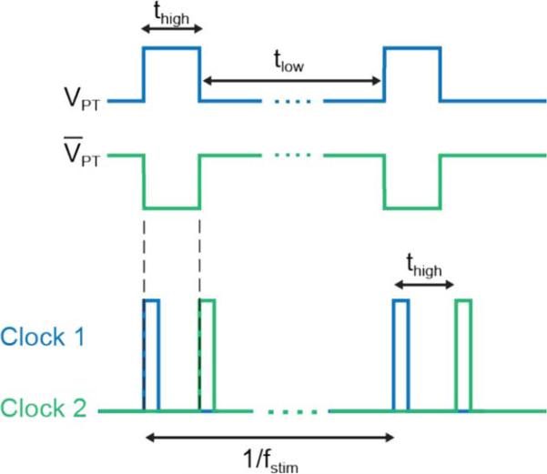
Since these two blocks function in an integrated fashion to provide control signals for a current stimulator, we begin by describing the main signals of interest followed by a detailed description of each block. The main output of the current-to-frequency converter block is VPT, a frequency modulated pulse train with an adjustable pulse-width. Fig. 5 depicts the duration that VPT is high and low, thigh and tlow respectively. The rising edge VPT triggers Clock 1 in the subsequent clock generation block. Similarly, the rising edge of V̄PT triggers Clock 2. As a result, the frequency of VPT determines the pulse rate, fstim. The PD of the target biphasic pulse is controlled in the clock generation block. The IPG is determined by the delay between Clock 1 and Clock 2, thigh, less the PD.
Fig. 5.
Pulse timing control. The signal VPT is output from the current-to-frequency converter block with a pulse rate of fstim. The rising edge of VPT triggers Clock 1 in the clock generation block. The clock generation block also controls the PD, the duration of each clock. The delay between the clocks, thigh, less the PD is the IPG.
a) Current-to-Frequency Converter Block [Fig. 4(b)]
The circuit is a modified version of a self-resetting neuron circuit [17] where the main signal of interest is VPT. The bias voltage Vbias2 controls the discharge current I8 through M8 and M9 when M9 is on. As a result Vbias2 controls thigh. Alternatively, tlow is affected by I3 since it controls how fast C1 (4 pF) and C2 (2 pF) are charged up. Another parameter affecting thigh is Vbias1, as it determines how fast VPT makes the low to high transition. The relationship between fstim and I3 is
| (3) |
For t >> thigh, it can be shown that
| (4) |
The linear relationship between fstim and I3 enables I3 to have the same dependence on angular velocity as fstim expressed in (1). When examining (3) it appears that at high pulse rates the linear assumption may be inaccurate. Consider an fstim of 450 pps and tlow = 10(thigh). Thus, 200 μs may be dedicated to the PD and IPG of a biphasic pulse. Given that most PDs are 100–200 μ s and that the IPG does not affect response to electrical stimulation of vestibular nerve fibers [12], it is reasonable to assume that the linearity assumption would not be grossly violated. However if necessary, Vbias2 may be dynamically controlled through a feedback circuit to maintain a small rending the term negligible. As a result the needed linearity can be realized.
b) Clock Generator Block [Fig. 4(c)]
Two fully digital clock generation circuits constitute this block generating Clock 1 and Clock 2, each with a frequency of fstim. The goal of each circuit is to create a pulse at the rising edge of its respective input and set the duration of each pulse [18]. To give the two clocks a phase difference, Clock 1 is generated directly from the pulse train obtained at the previous block, VPT. Clock 2 is generated from the inverse of that pulse train, V̄PT. When VPT is low, Clock 1 is also low. During that period, M10 keeps VX high. When makes a low-to-high transition, because M11 allows current flow, a discharge path is created that decreases VX. During that phase, Clock 1 is at high. When VX reaches the low value for the AND gate, Clock 1 also goes down to low. At that instant, M11 turns off, disconnecting the discharge path. The pulse-width of Clock 1 is related to how fast VX goes down to zero, which is effectively controlled by Vpulsel. The circuit for Clock 2 operates similarly and the pulse duration is controlled by Vpulse2.
IV. Measurement Results
To observe the pulse rate as a function of angular velocity, the signal processor was driven by a commercial gyroscope. Rotated about its z-axis, the gyroscope exhibited a sensitivity of 2 mV/°/s over a full-scale range of ±500 °/s, with a reference voltage of 1.35 V (InvenSense Inc., Sunnyvale, CA). Using a single-axis rate table (Ideal Aerosmith LLC, Pittsburgh, PA), the gyroscope was subjected to 33 sinusoidal rotations with angular velocity magnitudes that varied between 0°/sec and 500°/sec in 15°/sec increments. Pulse rate data was captured from an oscilloscope and processed using MATLAB software (The Math-Works Inc., Natick, MA) running on a PC. Discrete angular velocities were required since we were limited by the data transfer rate between the oscilloscope and the PC. Approximately 75 data points were obtained for each rotation. To find the pulse rate in the positive direction, the three maximum frequency values were averaged. Similarly, to find the pulse rate in the negative direction, the three minimum frequency values were averaged.
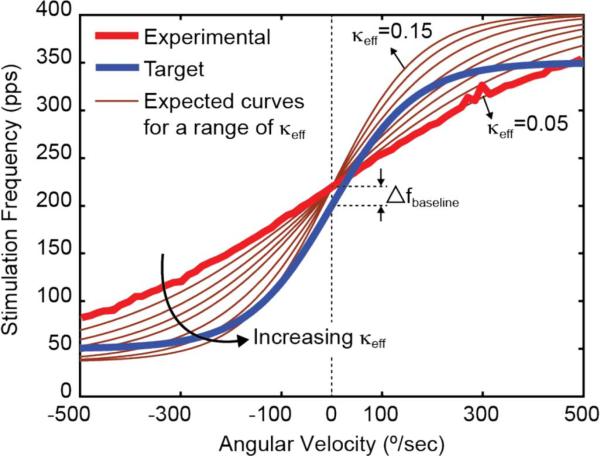
Fig. 6 compares the target and experimental versus angular velocity. To better understand the difference between the two curves we consider the three aspects of the curve relating pulse rate to angular velocity; the steepness, the baseline frequency (the frequency corresponding to zero angular velocity in the plane of measurement), and the frequency range.
Fig. 6.
Stimulation frequency versus angular velocity. The experimental stimulation frequency (pulse rate) as a function of angular velocity is shown. Superimposed on the plot is a a series of curves illustrating fstim versus angular velocity for κeff (0.05–0.15). The steepness of the curve is controlled by the κeff of the FGOTA. The baseline frequency difference between the experimental and the target curves, Δfbaseline, can be adjusted by decreasing (controlled by Vcontrol). To control the stimulation frequency range, the following values can be adjusted: the bias current of the FGOTA, Ibias, and the current ratio of the mismatched current mirror, I3 / I2(2), and the capacitance C2 (3).
The steepness of the output curve is controlled by the transconductance of the FGOTA (voltage-to-current converter). To characterize the linearity and the transconductance of the FGOTA, we varied Vout from 0–2.4 V. For a bias current of, Ibias = 3 nA, the measured linear range for 5% degradation in transconductance of the FGOTA is between 0.31 V and 0.37 V, when Vout ranges between 0.27 V and 2.13 V. The data reveals that the transconductance of the FGOTA is only slightly dependent on Vout and is ~3 nS. The transconductance of the FGOTA is mainly dependent on the κeff [κ * α term in (2)]. This is verified by a series of curves illustrating fstim versus angular velocity for a range of κeff from 0.05 to 0.15 (Fig. 6). As expected from (2), the steepness of the curve increases with κeff. At κeff = 0.05 the expected curve closely matches the experimental curve. Yet, the κeff corresponding to the target curve is around 3 times larger than that (~0.15). There are two reasons why the κeff is bound to small values. First, the κ of a transistor, in the FGOTA, in the weak inversion region is smaller than when in the strong inversion region. Second, the capacitive divider at the floating gates of the FGOTA reduces α to significantly low values, slightly lower than 1/9 considering the gate capacitances of M2 and M3.
The second aspect is the baseline frequency, fbaseline. This frequency is effectively controlled by the DC value, I1, added to Iout in Fig. 4(a). By changing (controlled by ), the difference between the baseline frequencies of the two curves ( Δfbaseline = 19.5 pps in Fig. 6) can be adjusted.
The last aspect we consider is the frequency range. This is controlled by three factors: the capacitance C2 (3), the bias current of the FGOTA, Ibias, and the current ratio of the mismatched current mirror, I3/I2. By varying any of these, the experimental curve can be adjusted to maintain within the desired stimulation frequency range.
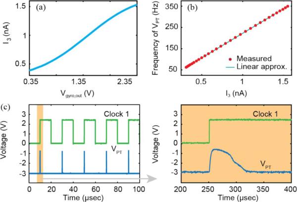
Fig. 7. summarizes critical outputs from the signal processor blocks. Fig. 7(a) illustrates the non-linearI3 response to Vgyro,out generated by the voltage-to-current converter block. In Fig. 7(b), a linear fstim versus I3 response is exhibited by the current-to-frequency converter block. And finally, in Fig. 7(c), the triggering of Clock 1 by the rising edge of VPT is shown.
Fig. 7.
Summary of signal processor block level outputs. (a) Non-linear response to Vgyro,out generated by the voltage-to-current conversion block. (b) Linear fstim versus I3 response is exhibited by the current-to-frequency conversion block with thigh = 200 μs. (c) Triggering of Clock 1 by the rising edge of VPT. Note that a long (10 ms) clock pulse was created in the clock generation block to illustrate the relationship between the rising edge VPT of and Clock 1. In practice the pulse duration of Clock 1 would be less than the duration of VPT.
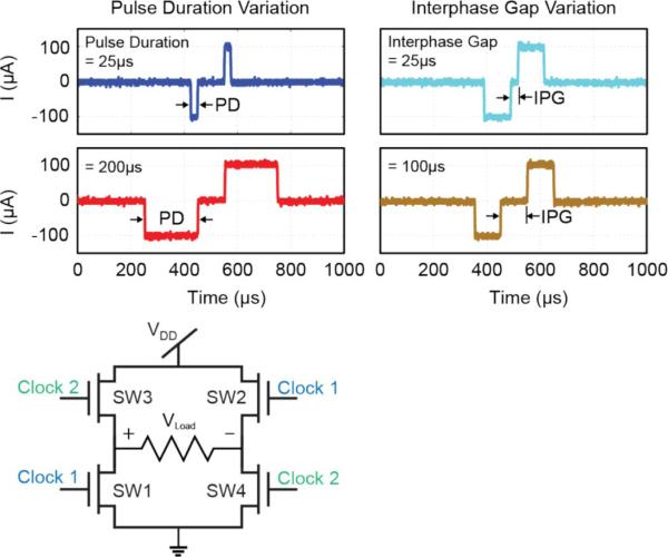
To demonstrate biphasic pulse control a 1 kΩ resistive load was placed across an H-bridge circuit (Fig. 8). Although this is voltage-based stimulation, it served to illustrate the ability of the signal processor to accurately control biphasic pulses ultimately generated by a current stimulator. When connected to a 2.4 V supply, a current level of 100 μA was obtained. Pulse durations of anodic and cathodic phases between 25–400 μs, and an inter-phase gap between 25–250 μs were observed. Hence all timing segments of a biphasic pulse can be controlled well within the necessary ranges.
Fig. 8.
Biphasic pulse control. Using a 1 kΩ resistive load placed across an H-bridge circuit, Clock 1 and Clock 2 serve to control a cathodic-first, symmetric, biphasic pulse. Representative values of the PD and IPG are demonstrated.
To appreciate the power demands of the signal processor circuitry, estimates are reported for a 350 Hz pulse rate with a 100 μsec PD. The voltage-to-current converter block consumes 0.48 μW. The combined power required by the current-to-frequency converter block and the clock generator block is mostly due to the dynamic power consumed at the digital gates. Ignoring any short circuit or leakage currents, and assuming a line capacitance of 2 pF for each interconnect line [13], the total power consumption of these is ~44 nW. The necessary switch circuitry consumes an additional 16.8 μW resulting in 18.324 μW. The use of a 14-bit AD5380 DAC (Analog Devices, Inc., Norwood, MA) for setting the six bias voltages consumes 12 mW max. Although the off-chip DAC facilitated circuit prototyping, in practice such bias voltages would be generated on the FPAA. Schlottmann and Hasler illustrate a method for creating voltage references through trapping different amount of charges at the floating gates of a FGOTA [19]. Precisely controllable (< ± mV) bias voltages from rail-to-rail (0–2.4 V) can be generated and will consume very little power, on the order of W.
V. Discussion
The goal of this work was to implement a vestibular signal processor on a reconfigurable FPAA platform. While we employed a hyperbolic tangent encoding angular velocity to pulse-rate, ongoing studies suggest there are alternative models for mapping between angular velocity to pulse rate [7], [12], [20]. The reconfigurability of the FPAA is an attractive feature for rapid mapping of modifications. Changes may be made to the voltage-to-current converter block alone, while retaining the existing current-to-frequency and clock generation blocks respectively. For example, to efficiently approximate the mean operating characteristics of vestibular nerve afferent fibers, a piece-wise linear (PWL) velocity-to-pulse rate mapping may be employed [12]. To realize this encoding the voltage-to-current converter block could consist of (1) an FGOTA that performs a nearly linear conversion of Vgyro,out to Iout; (2) an nMOS, to add a DC offset and thereby ensure Iout positive for all Vgyro,out; (3) a current-mode circuit realizing a PWL function [21], [22]; and (4) a current mirror to scale up/down the current output from the PWL circuit.
In addition to the benefit of reconfigurability, the FPAA presents a power advantage. We estimate that when bias voltages are generated on-chip, less than 20 μW will be consumed for a single canal system. As a comparison, Constandinou et al. predict a power consumption value of 48.84 μW, based on the simulation results of their semicircular canal processor ASIC [9]. Thus with respect to power the FPAA approach is attractive.
Another important consideration is signal processing for multi-canal system. Using the RASP 2.8 chip, a single-canal signal processor consumes nearly 70% of the chip area but not necessarily 70% of the circuitry. Because CABs include only nFETs or pFETs, it was essential to use circuit elements distally located on the chip. Thus interconnect lines were consumed rendering functional CABs unavailable. Interconnect was also consumed for testing purposes to probe signals by routing them to input/output pins. We estimate that at best a two-canal system could be realized with the RASP 2.8.
To effectively meet the needs for a vestibular signal processor, a future version of the RASP FPAA could be modified in the following ways. First, to better approach steep curves for the velocity-to-pulse rate mapping, additional FGOTAs with different κeff’s could be provided. This can be assured by the use of different capacitive divider ratios at the floating gates of the input transistors of the new FGOTAs. Second, when considering a PWL mapping, a wide-range FGOTA could be added to enable a linear Vgyro,out to Iout conversion. Third, to prevent inefficient interconnect usage, CABs could be altered internally to prevent distant connections. It could be advantageous to consider a more natural interconnection between the CABs such as in a lattice network [23].
VI. Conclusion
In this work we explored an FPAA-based vestibular signal processor. We demonstrated a single-canal system in which a voltage output from a rotated gyroscope was encoded into frequency modulated control signals for a current stimulator. We also discussed some limitations in scaling the RASP 2.8 FPAA to a multi-canal system. More broadly, this implementation demonstrated the utility of processing signals in the analog domain. Parallel to vestibular prostheses, low-power signal processing approaches for cochlear prostheses explore analog signal processing [24], [25]. Furthermore, while a custom ASIC yields a smaller footprint of ~1 mm2 [9], than the RASP 2.8 FPAA of ~166 cm2, the option for reconfigurability is advantageous. Serving as a development platform, an FPAA enables rapid revision of encoding schemes during testing in animal models. Given the need to optimize the tradeoff between dynamic range and axis misalignment (unintended stimulation), it may be necessary to adjust mapping and baseline pulse rate on an individual basis. Thus our proposed signal processing development platform may provide a measure of the programmability space needed for a fully implantable device.
In summary, through continued innovative and collaborative efforts along the lines of optimizing encoding, low-power sensing and circuitry, as well as enhanced stimulating electrode design for focused stimulation, an attractive therapeutic option may soon be available for individuals suffering from debilitating bilateral vestibular hypofunction.
Acknowledgment
The authors would like to thank the anonymous reviewers who provided important comments and suggestions on this work. They also thank Prof. J. Hasler and S. Brink at the Georgia Institute of Technology for access to FPAA hardware and valuable circuit design insight on how to best exploit their FPAA architecture for vestibular prosthesis circuitry. In addition, the authors thank Prof. F. Ayazi, W.-K. Sung, and D. Serrano for their help with rate table testing, as well as exploring interface circuitry for an alternative low-power gyroscope sensor (Qualtré, Inc., Marlborough, MA).
This work was supported in part by the National Science Founda tion under Grant ECCS-0927103, CAREER ECCS-1055801, and by PHS Grant UL1 RR025008, KL2 RR025009 from the Clinical and Translational Science Award program, National Institutes of Health, National Center for Research Resources. This paper was recommended by Associate Editor J. Georgiou.
Biography
 Hakan Töreyin (S'11) received the B.S. degree in electrical and electronics engineering from Middle East Technical University, Ankara, Turkey, and the M.S. degree in electrical and computer engineering from the Georgia Institute of Technology, Atlanta, in 2007 and 2008, respectively.
Currently, he is working toward the Ph.D. degree at the Georgia Institute of Technology. His research interests include interface circuit design for biomedical devices and low-power analog circuits design.
 Pamela Bhatti (M'05) received the B.S. degree in engineering science (bioengineering) from the University of California, Berkeley, the M.S. degree in electrical engineering from the University of Washington, Seattle, and the Ph.D. degree in electrical engineering, with an emphasis on micro-electro mechanical systems (MEMS), from the University of Michigan, Ann Arbor, in 1989, 1993, and 2006, respectively.
She is an Assistant Professor in the School of Electrical and Computer Engineering, Georgia Institute of Technology, Atlanta. Before completing her Ph.D. degree, she researched the detection of breast cancer with ultrasound imaging at the University of Michigan’s Department of Radiology (1997–1999). Her industry experience includes embedded systems software development at Microware Corporation, Des Moines, IA (1996–1997), local operating network applications development and customer support at Motorola Semiconductor, Austin, TX (1994–1995), and research and fabrication of controlled-release drug delivery systems at Alza Corporation, Palo Alto, CA (1986–1990).
Dr. Bhatti received the NSF Career Award in 2011. Committed to translating technology to the clinical setting, she is a KL2 Scholar with the Atlanta Clinical and Translations Sciences Institute.
REFERENCES
- 1.Herdman SJ. Vestibular Rehabilitation. 3rd ed. Davis; Philadelphia, PA: 2007. p. 2. [Google Scholar]
- 2.Wall C, III, Merfeld DM, Rauch SD, Black FO. Vestibular prostheses: The engineering and biomedical issues. J. Vestib. Res. 2002;12(2–3):95–113. [PubMed] [Google Scholar]
- 3.Gong W, Merfeld DM. System design and performance of a uni-lateral horizontal semicircular canal prosthesis. IEEE Trans. Biomed. Eng. 2002;49(2):175–181. doi: 10.1109/10.979358. [DOI] [PubMed] [Google Scholar]
- 4.Merfeld DM, Haburcakova C, Gong W, Lewis RF. Chronic vestibulo-ocular reflexes evoked by a vestibular prosthesis. IEEE Trans. Biomed. Eng. 2007;54:1005–1015. doi: 10.1109/TBME.2007.891943. [DOI] [PubMed] [Google Scholar]
- 5.Della Santina CC, Migliaccio AA, Patel AH. A multichannel semicircular canal neural prosthesis using electrical stimulation to restore 3-D vestibular sensation. IEEE Trans. Biomed. Eng. 2007 Jun;54(6):1016–1030. doi: 10.1109/TBME.2007.894629. [DOI] [PMC free article] [PubMed] [Google Scholar]
- 6.DiGiovanna J, Gong W, Haburcakova C, Kögler V, Carpaneto J, Genovese V, Merfeld DM, Demosthenous A, Guyot J-P, Hoffmann K-P, Berthoz A, Morari M, Micera S. Development of a closed-loop neural prosthesis for vestibular disorders. J. Automat. Control. 2010;20:27–32. [Google Scholar]
- 7.Chiang B, Fridman GY, Dai C, Rahman MA, Della Santina CC. Design and performance of a multichannel vestibular pros-thesis that restores semicircular canal sensation in rhesus monkey. IEEE Trans. Neural Syst. Rehabil. Eng. 2011 Oct;19(5):588–598. doi: 10.1109/TNSRE.2011.2164937. [DOI] [PMC free article] [PubMed] [Google Scholar]
- 8.Constandinou TG, Georgiou J, Toumazou C. A partial-currentsteering biphasic stimulation driver for vestibular prostheses. IEEE Trans. Biomed. Circuits Syst. 2008 Jun;2(2):106–113. doi: 10.1109/TBCAS.2008.927238. [DOI] [PubMed] [Google Scholar]
- 9.Constandinou TG, Georgiou J, Toumazou C. A neural implant ASIC for the restoration of balance in individuals with vestibular dys-function. Proc. IEEE Int. Symp. Circuits and Systems. 2009 May;:641–644. [Google Scholar]
- 10.Jiang D, Demosthenous A, Perkins T, Xiao L, Donaldson N. A stimulator ASIC featuring versatile management for vestibular pros-theses. IEEE Trans. Biomed. Circuits Syst. 2011 Apr;5(2):147–159. doi: 10.1109/TBCAS.2011.2138139. [DOI] [PubMed] [Google Scholar]
- 11.Shkel A, Zeng F-G. An electronic prosthesis mimicking the dyanmic vestibular function. Audiol. Neurotol. 2006;11:113–122. doi: 10.1159/000090684. [DOI] [PubMed] [Google Scholar]
- 12.Davidovics NS, Fridman GY, Chiang B, Della Santina CC. Effects of biphasic current pulse frequency, amplitude, duration, and interphase gap on eye movement responses to prosthetic electrical stimulation of the vestibular nerve. IEEE Trans. Neural Syst. Rehabil. Eng. 2011 Feb;19(1):84–94. doi: 10.1109/TNSRE.2010.2065241. [DOI] [PMC free article] [PubMed] [Google Scholar]
- 13.Basu A, Brink S, Schlottmann C, Ramakrishnan S, Petre C, Koziol S, Baskaya F, Twigg C, Hasler P. A floating-gate-based field-programmable analog array. IEEE J. Solid-State Circuits. 2010 Sep;45(9):1781–1794. [Google Scholar]
- 14.Anadigm [May 2010];Dynamically Programmed Analog Signal Processors [Online] Available: http://www.anadigm.com/dpasp.asp.
- 15.Gwilliam J, Horch K. A charge-balanced pulse generator for nerve stimulation applications. J. Neurosci. Methods. 2008;168(1):146–150. doi: 10.1016/j.jneumeth.2007.09.004. [DOI] [PubMed] [Google Scholar]
- 16.Basu A, Ramakrishnan S, Petre C, Koziol S, Brink S, Hasler PE. Neural dynamics in reconfigurable silicon. IEEE Trans. Biomed. Circuits Syst. 2010 Oct;4(5):311–319. doi: 10.1109/TBCAS.2010.2055157. [DOI] [PubMed] [Google Scholar]
- 17.Mead C. Analog VLSI and Neural Systems. Addison-Wesley; Reading, MA: 1989. pp. 198–200. [Google Scholar]
- 18.Mukhopadhyay S. Class Notes for ECE 6130, Feb. 13, 2008, Sequential Elements. Department of Electrical and Computer Engineering, Georgia Institute of Technology; [Google Scholar]
- 19.Schlottmann C, Hasler P. A highly dense, low power, programmable analog vector-matrix multiplier: The FPAA implementation. IEEE J. Emerging Selected Topics Circuits Syst. 2011;1(3):403–411. [Google Scholar]
- 20.Fridman GY, Davidovics NS, Dai C, Migliaccio AA, Della Santina CC. Vestibulo-ocular reflex responses to a multichannel vestibular prosthesis incorporating a 3D coordinate transformation for correction of misalignment. J. Assoc. Res. Otolaryngol. 2010 Sep;11(3):367–381. doi: 10.1007/s10162-010-0208-5. [DOI] [PMC free article] [PubMed] [Google Scholar]
- 21.Ramirez-Angulo J, Sanchez-Sinencio E, Rodriguez-Vazquez A. A piecewise linear function approximation using current mode circuits. Proc. IEEE Int. Symp. Circuits and Systems. 1992:2021–2024. [Google Scholar]
- 22.Bhat MS, Rekha S, Jamadagni HS. Extrinsic analog synthesis using piecewise-linear current-mode circuits. Proc. Int. Conf. Very-Large-Scale Integration Design. 2006:51–56. [Google Scholar]
- 23.Becker J, Henrici F, Trendelenburg S, Ortmanns M, Manoli Y. A field-programmable analog array of 55 digitally tunable OTAs in a hexagonal lattice. IEEE J. Solid-State Circuits. 2008 Dec;43(12):2759–2768. [Google Scholar]
- 24.Georgiou J, Toumazou C. A 126 W cochlear chip for a totally implantable system. IEEE J. Solid-State Circuits. 2005;40(2):430–443. [Google Scholar]
- 25.Mandal S, Zhak SM, Sarpeshkar R. A Bio-inspired active radio frequency silicon cochlea. IEEE J. Solid-State Circuits. 2009;44(6):1814–1828. [Google Scholar]


