Abstract
This letter presents a graphene field effect transistor (GFET) nanosensor that, with a solid gate provided by a high-κ dielectric, allows analyte detection in liquid media at low gate voltages. The gate is embedded within the sensor and thus is isolated from a sample solution, offering a high level of integration and miniaturization and eliminating errors caused by the liquid disturbance, desirable for both in vitro and in vivo applications. We demonstrate that the GFET nanosensor can be used to measure pH changes in a range of 5.3–9.3. Based on the experimental observations and quantitative analysis, the charging of an electrical double layer capacitor is found to be the major mechanism of pH sensing.
Graphene is a two-dimensional nanomaterial consisting of a single layer of carbon atoms arranged in hexagonal crystalline form, and its unique properties have been exploited to enable biosensors that are based on electric,1 optical,2 electrochemical,3,4 and other principles. In particular, graphene has been used to form a conducting channel in field effect transistors (FETs), allowing highly sensitive electric detection of analytes. Such graphene FET (GFET) sensors, when operating in liquid media, are generally constructed in a solution-gated or solid-gated configuration. In a solution-gated GFET sensor,5 a reference electrode is inserted into the electrolyte solution that is in contact with graphene to serve as the gate electrode, while the electric double layer (EDL)6 formed at the solution-graphene interface plays the role of the gate dielectric. Using various compositions of an electrolyte solution or graphene-immobilized functional groups, such sensors have been used to demonstrate the detection of physicochemical parameters such as pH5 and metallic ions,7 and biochemical analytes such as DNA6 and protein.8 These solution-gated sensors typically require an external electrode inserted into the electrolyte solution, which hinders the integration and miniaturization of the device. In addition, the gate capacitance or the capacitance across the EDL dielectric layer is susceptible to disturbances in liquid media, which can result in fluctuations in electrical measurements of properties of graphene including the position of the Dirac point.9 In contrast, in a typical solid-gated GFET,10 the gate capacitance is provided by a SiO2 dielectric layer sandwiched between graphene and the underlying silicon substrate, which serves as the gate electrode. By eliminating the need for the external wire insertion into the electrolyte solution, solid-gated sensors can be highly miniaturized and integrated. However, due to the intrinsically low capacitance of the SiO2 layer, usually the solid-gated GFET sensors require undesirably high gate voltages (40–50 V),11,12 consequently impeding their application to biosensing in liquid media.
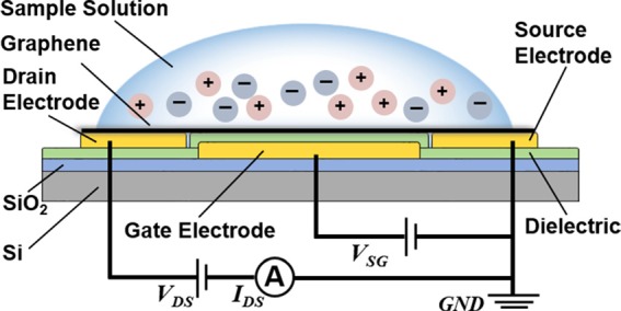
This paper presents a GFET nanosensor in liquid media using a thin layer of HfO2 with a high dielectric constant (κ) as a gate dielectric layer. The HfO2 layer is sandwiched between the conducting-channel graphene and a gate electrode (Figure 1) and is hence embedded within the sensor. This enables a high level of integration in the construction and passivation of electrically conducting elements in the sensor, as is highly desirable for analyte detection in liquid media. The use of the high-κ dielectric material (HfO2) provides two orders of magnitude higher specific capacitance than conventional SiO2 solid-gated sensors, thereby rendering high transconductance and allowing the device to operate at low gate voltages. In addition, the gate dielectric is isolated from the liquid media, thus eliminating errors caused by disturbances (e.g., bulk motion of sample solution). Furthermore, the sensor is amenable to time- and cost-effective microfabrication using photolithography without the need for manual assembly of discrete components (e.g., electrodes) with graphene, thereby simplifying the fabrication process. We demonstrate the pH sensing using this high-κ GFET nanosensor. Experimental results show that the device is capable of measuring pH in a range of 5.3 to 9.3 with a sensitivity of ∼57.6 mV/pH and at a gate voltage of less than 1.5 V, which is approximately a factor of 30 lower than that used in SiO2 solid-gated sensors. We also elucidate the mechanism of pH-dependent changes in graphene conductivity by representing the nanosensor as a dual-gated FET.
FIG. 1.

Schematic of the graphene-based FET nanosensor. Graphene serves as the conducting channel, while a 20-nm-thick HfO2 layer between the graphene and the substrate-supported gate electrode serves as the dielectric layer.
The nanosensor is configured as a solid-gated FET device, in which a graphene sheet, serving as the conducting channel, connects the source and drain electrodes on a HfO2 dielectric layer, which in turn lies above the gate electrode on the substrate (Fig. 1). When a buffer solution is introduced onto the graphene surface, the carrier concentration in the bulk of the graphene undergoes a change due to variations in the electric potential in the buffer next to the graphene. Since the magnitude of the electric potential depends on the ion concentration (e.g., H+), the pH level can be determined by measuring the graphene's electric properties such as its transfer characteristics and conductance, which is directly related to the carrier concentration. To allow a high level of integration while avoiding the need for high gate voltages, the nanosensor uses 20 nm thick HfO2, a material with a high dielectric constant (κ ≈ 20, compared to κ ≈ 3.9 for SiO2), as the dielectric layer to provide a high gate capacitance (∼1 μF/cm2). This, in general, allows the Dirac point, at which the drain-source current IDS achieves its minimum, to be observed at a lower gate voltage.11
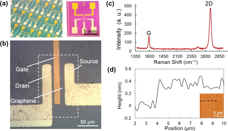
The nanosensor (Figure 2(a)) was fabricated on a SiO2-coated silicon substrate by first depositing and patterning the gate electrodes (Cr/Au 5/45 nm). Subsequently, a 20 nm HfO2 layer was deposited over the wafer using atomic layer deposition (ALD). A lift-off process was used to create the drain and source electrodes, onto which a single-layer graphene sheet synthesized by chemical vapor deposition (CVD) was transferred (Figure 2(b)). A microchamber (2.5 μl), fabricated in a polydimethylsiloxane (PDMS) sheet via soft lithography, was placed on the resulting nanosensor chip to confine sample liquid on the device. Further details of the device fabrication process are provided in supplementary material.13
FIG. 2.
Micrographs of graphene nanosensors: (a) Multiple devices batch-fabricated on the same substrate (left) and close-up view of a single device (right). (b) Detailed view of the source, drain, and gate electrodes. Dashed box approximately indicates the region covered by graphene. (c) Raman spectrum of the graphene. (d) AFM measurements of the graphene thickness. Inset: AFM photo of graphene whose thickness was measured along the dashed line.
We first used Raman spectroscopy and atomic force microscopy (AFM) to confirm that the graphene used to fabricate the device consisted of a single atomic layer. The Raman spectrum revealed G mode and 2D mode, which are the characteristic of single-layer graphene (Figure 2(c)). AFM data were used to determine the thickness of the graphene to be 0.3–0.4 nm (Figure 2(d)), which reflects the van der Waals diameter of carbon and is hence also indicative of single-layer graphene.
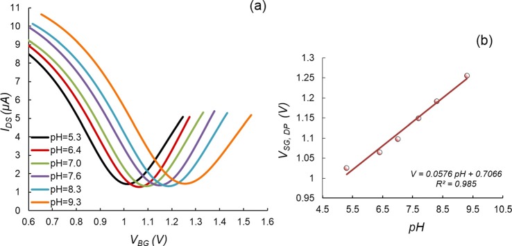
We then investigated the transfer characteristics of bare graphene in air. IDS was measured while the solid-gate voltage VSG, which makes a major contribution to the overall gate voltage (below), was varied sinusoidally from −0.2 to 1.9 V. An ambipolar curve was observed; the Dirac point solid-gate voltage, or the gate voltage value at which the IDS achieves the minimum (Figure S2(a)),13 was hence determined to be VSG,DP = 0.7 V. This confirmed that the conductivity of the graphene was being altered by the field effect. We next tested our nanosensor for pH sensing in liquid media. Samples at various pH values (5.3 to 9.3) were prepared by mixing NaOH or HCl with phosphate buffered saline (PBS) buffer (Life Technologies, ionic strength of ∼150 mM). A sample solution was incubated with our nanosensor, during which IDS values were measured while the gate voltage VBG was swept from 0.6 V to 1.6 V. We found that VSG,DP < 1.5 V at all pH levels (Fig. 3). These significantly reduced gate voltage values, compared to 40–50 V for SiO2 based solid-gated sensor, can be attributed to the high gate capacitance and hence the high transconductance provided by the high-κ HfO2 dielectric layer. VSG,DP was found to linearly increase with the pH value at a sensitivity of ∼57.6 mV/pH (Fig. 3(a)), which would otherwise not be attainable by a conventional dielectric (SiO2)-based device operating at similarly low gate voltages. We have also determined that these measurements were reproducible, with a different device of the same design yielding a closely agreeing sensitivity of 58.2 mV/pH (Figure S3).13 When pH increases, the electrostatic potential above graphene increases due to the decrease of H+ (see below); therefore, the curve shifts to the right to compensate for the increase in the electrostatic potential. The leakage current between drain/source and gate electrodes was found to be much smaller than IDS and therefore negligible.
FIG. 3.

Dependence of the nanosensor characteristics on pH. (a) Transfer characteristic curves obtained at varying pH values. The VSG, DP shifts linearly to higher gate voltages with increasing pH (57.6 mV/pH). (b) Dependence of the Dirac point voltage on pH. The solid line represents a linear fit.
There are two possible physical processes that have been used to explain how adsorption of ions on graphene causes variations in the conductivity.14 The first process involves the charging of the EDL capacitor by adsorbed ions, thereby causing variations in the potential in the solution in contact with the graphene, and therefore changing the Fermi level and carrier density of graphene, e.g., the electric field tuning.15 In the second process, which is known as surface charge transfer doping,14 adsorbed ions serve as dopants, from which electrons are exchanged into or out of the bulk of the graphene. Our solid-gated sensor, which avoids the influence of the externally applied top gate voltage on the EDL, can be used to investigate the effect of either the EDL capacitor charging or the surface charge transfer doping. From the transfer characteristics obtained at different pH levels (Figure 3(a)), the transconductance was found to be within 0.3 μS of a constant value of 23.2 μS (Figure S2(b)),13 implying that the carrier mobility was also approximately a constant regardless of the pH variations. Therefore, the surface transfer doping is not a dominant effect, which would otherwise have altered the carrier mobility significantly.12 This is in agreement with the study by Xia16 and Mailly-Giacchetti.17
On the other hand, to investigate the effect of the charging of the EDL capacitor, our sensor can be modeled as a dual-gate field effect transistor consisting of the solid gate (with HfO2 as the dielectric) below the graphene and a solution gate formed by the EDL above the graphene at its interface with the solution. The voltage on the top solution gate, VLG, which is equal to the potential drop across the EDL capacitor, depends on the ion concentration in the electrolyte solution. This solution gate voltage, which leads to the charging of the EDL capacitor, can be estimated by the Nernst equation,18 VLG = E0 − 2.3 log(H+)RT/nF, where E0 is a constant reference potential, R is the universal gas constant, T is the temperature of 298.15 K, n is the ionic charge (1 for H+), and F is the Faraday constant. With pH = −log(H+), we obtain
| (1) |
Thus, the highly linear dependence of the experimentally determined VSG,DP on pH (Fig. 3(b)) allowed us to conclude that the right shift of VSG,DP with pH is due to the increase in VLG. In addition, it was seen that VSG,DP depended on VLG in a roughly linear manner in the pH range tested (Figure S4).13 As the slope of this dependence (estimated to be ∼1) is equal to the ratio of the solution-gate capacitance (CLG) to the solid-gate capacitance (CSG),19,20 CLG/CSG ≈ 1. That is, the solid-gate capacitance was comparable to the liquid-gate capacitance21 (typically on the order of 1 μF/cm2) in our nanosensor, representing a significance improvement over SiO2 solid-gated GFET devices. This allowed the nanosensor to operate at the low gate voltages as demonstrated. In addition, it should be noted that at a given pH level, a significant increase in the ionic strength of alkali cations (e.g., Na+ and K+) may decrease the measurement sensitivity.22 This is because the electrostatic gating effects produced by the alkali cations compete with the gating effects from the H+. Therefore, to measure the concentration of H+, the concentration of the nonspecific ions should be maintained at a constant level to obtain a constant sensitivity. Indeed, the concentrations of the alkali cations were approximately constant in our experiments, as the NaOH was added to the buffer at a very dilute concentration (∼0.1 mM) and hence had negligibly effects on the ionic strength of the buffer (150 mM). Therefore, the sensitivity in pH measurements was approximately constant and not affected by the addition of NaOH for control of pH values.
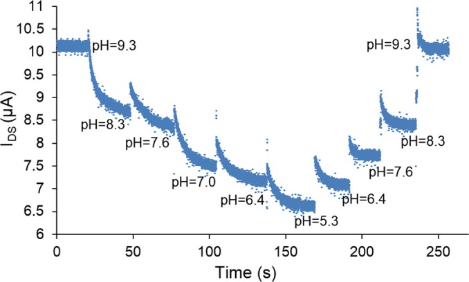
To demonstrate the ability of the nanosensor to perform real-time pH measurements, we measured IDS at a fixed gate voltage (VBG = 0.75 V), while successively introducing samples with different pH values (Fig. 4). As pH decreased from 9.3 to 5.3 (i.e., the solution becomes more acidic), the VTG also decreased (Eq. (1)) and the EDL capacitor accordingly underwent partial discharging. This caused a decrease in the carrier concentration of the graphene, and IDS hence correspondingly decreased. These phenomena were reversed as pH continued to change, but now in a reversed direction by increasing from 5.3 to 9.3. This reflected that the EDL capacitor underwent charging, thereby causing the carrier concentration in the graphene, and hence IDS, to increase. Throughout the entire set of measurements, the values of IDS were found to be consistent at a given pH value, regardless of whether this value was reached by pH increasing from a lower value or decreasing from a higher value, with small deviations attributable to the hysteresis in the electronic transport in the graphene.23 Thus, it was concluded that pH measurements by the nanosensor were reversible, which is important for practical applications.
FIG. 4.

Real time measurements of pH: the source-drain current IDS varied consistently and reversibly with pH at a fixed gate voltage (VBG = 0.75 V).
We have described a high-κ solid-gated GFET nanosensor in liquid media. The embedded solid gate eliminates the need for an external gate electrode and is hence amenable to the complete integration of the nanosensor as is highly desirable for analyte detection in liquid media. The use of a high-κ dielectric allows the device to operate at low gate voltages and avoids errors caused by gate capacitance variations. Experimental data from the nanosensor showed measurements of pH in a range of 5.3 to 9.3 with a sensitivity of ∼57.6 mV/pH. The pH-dependent electrical responses of the nanosensor responsible for the measurements were found to be caused by the charging of the electric double layer capacitor, rather than surface transfer doping. These results suggest that the GFET nanosensor can be potentially used to enable highly integrated sensing of chemical and biological analytes.
Acknowledgments
This work was partially supported by the National Institutes of Health (Award No. 1DP3 DK101085-01). We also appreciate the helpful discussions with Lei Wang and Xian Zhang from Columbia University. In addition, Yibo Zhu and Cheng Wang gratefully acknowledge the National Scholarships (Award Nos. 201206250034 and 201206200032) from the China Scholarship Council.
References
- 1.Cheng Z. G., Li Q., Li Z. J., Zhou Q. Y., and Fang Y., Nano Lett. 10(5), 1864 (2010). 10.1021/nl100633g [DOI] [PubMed] [Google Scholar]
- 2.Xu W. G., Ling X., Xiao J. Q., Dresselhaus M. S., Kong J., Xu H. X., Liu Z. F., and Zhang J., Proc. Natl. Acad. Sci. U. S. A. 109(24), 9281 (2012). 10.1073/pnas.1205478109 [DOI] [PMC free article] [PubMed] [Google Scholar]
- 3.Kang X. H., Wang J., Wu H., Liu J., Aksay I. A., and Lin Y. H., Talanta 81(3), 754 (2010). 10.1016/j.talanta.2010.01.009 [DOI] [PubMed] [Google Scholar]
- 4.Unnikrishnan B., Palanisamy S., and Chen S. M., Biosens. Bioelectron. 39(1), 70 (2013). 10.1016/j.bios.2012.06.045 [DOI] [PubMed] [Google Scholar]
- 5.Ohno Y., Maehashi K., Yamashiro Y., and Matsumoto K., Nano Lett. 9(9), 3318 (2009). 10.1021/nl901596m [DOI] [PubMed] [Google Scholar]
- 6.Ohno Y., Okamoto S., Maehashi K., and Matsumoto K., Jpn. J. Appl. Phys., Part 1 52(11), 110107 (2013). 10.7567/JJAP.52.110107 [DOI] [Google Scholar]
- 7.Maehashi K., Sofue Y., Okamoto S., Ohno Y., Inoue K., and Matsumoto K., Sens. Actuators, B 187, 45 (2013). 10.1016/j.snb.2012.09.033 [DOI] [Google Scholar]
- 8.Mao S., Lu G. H., Yu K. H., Bo Z., and Chen J. H., Adv. Mater. 22(32), 3521 (2010). 10.1002/adma.201000520 [DOI] [PubMed] [Google Scholar]
- 9.Schwierz F., Nat. Nanotechnol. 5(7), 487 (2010). 10.1038/nnano.2010.89 [DOI] [PubMed] [Google Scholar]
- 10.Yuan W. J. and Shi G. Q., J. Mater. Chem. A 1(35), 10078 (2013). 10.1039/c3ta11774j [DOI] [Google Scholar]
- 11.Kim B. J., Jang H., Lee S. K., Hong B. H., Ahn J. H., and Cho J. H., Nano Lett. 10(9), 3464 (2010). 10.1021/nl101559n [DOI] [PubMed] [Google Scholar]
- 12.Chen J. H., Jang C., Adam S., Fuhrer M. S., Williams E. D., and Ishigami M., Nat. Phys. 4(5), 377 (2008). 10.1038/nphys935 [DOI] [Google Scholar]
- 13.See supplementary material at http://dx.doi.org/10.1063/1.4916341E-APPLAB-106-030513 for further details of fabrication and measurements.
- 14.Ristein J., Science 313(5790), 1057 (2006). 10.1126/science.1127589 [DOI] [PubMed] [Google Scholar]
- 15.Williams J. R., Low T., Lundstrom M. S., and Marcus C. M., Nat. Nanotechnol. 6(4), 222 (2011). 10.1038/nnano.2011.3 [DOI] [PubMed] [Google Scholar]
- 16.Xia J. L., Chen F., Wiktor P., Ferry D. K., and Tao N. J., Nano Lett. 10(12), 5060 (2010). 10.1021/nl103306a [DOI] [PubMed] [Google Scholar]
- 17.Mailly-Giacchetti B., Hsu A., Wang H., Vinciguerra V., Pappalardo F., Occhipinti L., Guidetti E., Coffa S., Kong J., and Palacios T., J. Appl. Phys. 114(8), 084505 (2013). 10.1063/1.4819219 [DOI] [Google Scholar]
- 18.Feiner A. S. and Mcevoy A. J., J. Chem. Educ. 71(6), 493 (1994). 10.1021/ed071p493 [DOI] [Google Scholar]
- 19.Kim S., Nah J., Jo I., Shahrjerdi D., Colombo L., Yao Z., Tutuc E., and Banerjee S. K., Appl. Phys. Lett. 94(6), 062107 (2009). 10.1063/1.3077021 [DOI] [Google Scholar]
- 20.Meric I., Han M. Y., Young A. F., Ozyilmaz B., Kim P., and Shepard K. L., Nat. Nanotechnol. 3(11), 654 (2008). 10.1038/nnano.2008.268 [DOI] [PubMed] [Google Scholar]
- 21.Xia J. L., Chen F., Li J. H., and Tao N. J., Nat. Nanotechnol. 4(8), 505 (2009). 10.1038/nnano.2009.177 [DOI] [PubMed] [Google Scholar]
- 22.Heller I., Chatoor S., Mannik J., Zevenbergen M. A. G., Dekker C., and Lemay S. G., J. Am. Chem. Soc. 132(48), 17149 (2010). 10.1021/ja104850n [DOI] [PubMed] [Google Scholar]
- 23.Wang H. M., Wu Y. H., Cong C. X., Shang J. Z., and Yu T., ACS Nano 4(12), 7221 (2010). 10.1021/nn101950n [DOI] [PubMed] [Google Scholar]
Associated Data
This section collects any data citations, data availability statements, or supplementary materials included in this article.
Data Citations
- See supplementary material at http://dx.doi.org/10.1063/1.4916341E-APPLAB-106-030513 for further details of fabrication and measurements.


