Abstract
Metal-dielectric-metal (MDM) structures provide directional emission close to the surface normal, which offers opportunities for new design formats in fluorescence based applications. The directional emission arises due to near-field coupling of fluorophores with the optical modes present in the MDM substrate. Reflectivity simulations and dispersion diagrams provide a basic understanding of the mode profiles and the factors that affect the coupling efficiency and the spatial distribution of the coupled emission. This work reveals that the composition of the metal layers, the location of the dye in the MDM substrate and the dielectric thickness are important parameters that can be chosen to tune the color of the emission wavelength, the angle of observation, the angular divergence of the emission and the polarization of the emitted light. These features are valuable for displays and optical signage.
Keywords: Metal-Dielectric-Metal, Directional Emission, Dispersion, Surface-Plasmon-Coupled Emission, Cavity-Mode-Coupled Emission
Introduction
The interaction of fluorescence with metallic surfaces and nanostructures provides many interesting opportunities for tailoring emission properties.1 One important effect that can be achieved by fluorophore-plasmon coupling is the modification in the spatial distribution of fluorescence and conversion of the usual omnidirectional fluorescence to directional emission. Surface-plasmon-coupled emission (SPCE) is a remarkable phenomenon by which fluorophores placed at close distances from a thin metal film display emission over a small range of angles into the substrate.2–4 The use of this phenomenon for better fluorescence detection, immunoassays, bio-sensing and background reduction has been widely investigated.5–9 Despite these improvements, SPCE has a limitation because the emission occurs at angles larger than the critical angle of the glass/air interface. The appearance of the emitted light at large angles relative to the surface normal makes it difficult to collect the coupled emission and is unsuitable for high throughput or array-based applications.
Recently, we have considered the effects of an additional metal layer above the single metal-dielectric (MD) surface that is generally used in typical SPCE substrates.10,11 It was observed that in planar metal-dielectric-metal (MDM) substrates, the coupling of fluorescence to the Fabry-Pérot-like modes leads to the guiding of emission in a direction normal to the MDM substrate.10–13 The MDM substrates thus allow excitation with light that is perpendicular to the substrate plane and provide emission within a narrow angular distribution that is normal to the plane. The occurrence of beaming emission from such simple structures is an interesting result and can have many applications. The MDM structures can be readily adapted for use in microarray formats, for directional fluorescence studies with multiple probes, for bio-sensing and optical signage. Moreover, it is possible to tailor the emission from various dye molecules emitting in the NIR, visible or UV/blue region, in a simple and flexible manner by changing the design parameters of the MDM structure and the nature of the metallic layer.11
The observation of directional emission from MDM substrates, led us to investigate a combination of plasmonic and photonic structures.14 We have recently reported on the occurrence of emission normal to the surface of a hybrid structure consisting of a metal layer and a truncated 1-dimensional photonic crystal (1DPC), due to coupling with Tamm states (Tamm-state-coupled emission, TSCE).14,15 Knowledge of the existence of Tamm states is relatively new. These states appear between two adjacent 1DPCs with overlapping photonic band gaps or between a 1DPC and a metal film.16,17 The latter are also called Tamm plasmon polaritons.
In the light of these new results, we were encouraged to carry out further detailed investigations on the optical modes that exist in MDM structures. In the present study, we have simulated the reflectivity dispersion plots and electric field intensity distributions for these structures, to understand the factors that affect the coupling efficiency and the spatial distribution of emission from dye molecules within MDM substrates. In addition to nearly symmetric MDM substrates that are composed of the same metal in both the top and bottom layers, we have also considered MDM substrates with mixed metal layers as an attempt to control the color, intensity and angular divergence of the emitted light. The effect of dye location in determining the nature of the coupled emission observed from the MDM substrate has been studied. The present results and analyses will be valuable to interpret the fluorescence properties in various MDM substrates and to design suitable structures for future fluorescence applications.
Experimental Methods
Materials
The metals, Au and Ag (purity 99.999%), poly(vinylalcohol) (PVA, MW 13000-23000) and Sulforhodamine 101 (S101) were purchased from Sigma-Aldrich. Glass microscope slides were obtained from VWR.
Preparation of the MD and MDM substrates
The glass slides were cleaned by soaking in “piranha solution” overnight followed by washed thoroughly with distilled deionized water and dried with air stream. Metallic films (thickness ~50 nm) were deposited on the cleaned glass slides using an Edwards Auto 306 Vacuum evaporation chamber under high vacuum (< 5×10⁻⁷ Torr). The deposition rate (~1.0 nm/min) was adjusted by the filament current and the thickness of the deposited film was measured with a built-in quartz crystal microbalance. The surface of the metal film (Au or Ag) was then spin coated (at 3000 rpm) with an aqueous solution of PVA, containing about 100 μM of the dye, S101. The weight percentage of PVA was varied (~3.5–4%) to obtain the required thickness of the dielectric, PVA layer (~130–150 nm).10,11 We refer to this PVA coated metal film as a metal-dielectric (MD) structure (PVA-Ag-glass and PVA-Au-glass). To get the final symmetric or mixed-metal MDM substrates, a second metallic layer (50 nm) was added after the PVA layer, by thermal vapor deposition. The MDM substrates for the present study are: Ag-PVA-Ag-glass (I), Au-PVA-Au-glass (II), Ag-PVA-Au-glass (III) and Au-PVA-Ag-glass (IV) as depicted in Scheme 1.
Scheme 1.

Schematic of the metal-dielectric-metal (MDM) substrates used in the present study.
Fluorescence measurements
The MDM or MD samples were fixed to a hemicylindrical quartz prism using glycerol for refractive index matching. The prism along with the attached sample was placed on a precise rotary stage that allows excitation and observation at any angle relative to the vertical axis of the cylinder. The samples were illuminated from the air side using a continuous wave diode pumped solid state laser (CNI, China) with excitation wavelength 532 nm, incident normal to the surface. For MD substrates, the excitation light was incident on the top PVA layer containing the dye and for MDM substrates excitation was through the top metal film. A schematic of the illumination geometry is presented in Figure 1. An angle of 0° is perpendicular to the glass side of the sample while an angle of 180° is perpendicular to the air side. The emission was collected with an Ocean Optics optical fiber (diameter 1 mm and NA 0.22) and recorded on a spectrofluorometer (Ocean Optics SD2000). The excitation light was passed through laser clean-up filter and the emission was observed through a 550 nm long pass filter to suppress any scattered light. The S-polarized (TE, E-field parallel to the sample surface and out of the plane of Figure 1) and P-polarized (TM, E-field in the plane of incidence and of the plane of Figure 1) emissions were observed by changing the polarizer orientation in front of the fiber optic observation cable.
Figure 1.
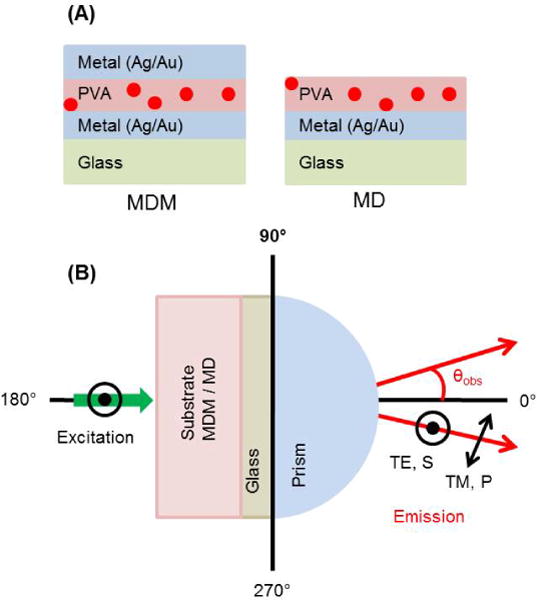
(A) Schematic of the metal-dielectric-metal (MDM) and metal-dielectric (MD) substrates. The dielectric (PVA) layer contains the dye molecules, S101. (B) Experimental geometry and polarizations used for the present measurements; the excitation laser (532 nm) is vertically polarized, which is normal to the plane of the paper.
Reflectivity calculations
Reflectivity and electric field intensity calculations were performed using the TF Calc. software package (Software Spectra, Inc., Portland, Oregon), based on the transfer matrix formalism. For all simulations, light (600 nm) was considered to be incident on the metal film from the glass side at different angles, to compare with the coupled emission from the dye S101 (emission maximum 600 nm) that is observed on the glass side (Figure 1).
Results and Discussion
The coupled emission observed for dye molecules in MDM substrates can be understood by studying the mode profiles of the MDM structures. Figure 2(A–C) shows the calculated angle-dependent reflectivity plots with 600 nm incident light, and the complete reflectivity dispersion diagrams, R(λ, θ), for the four MDM substrates, I–IV, used in the present study. Let us first examine the symmetric MDM substrate, Ag-PVA-Ag-glass (I), Figure 2(I: A). In this case, the most prominent dip in reflectivity for 600 nm incident light (both S- and P-polarized) appears at 0°, for a PVA film thickness of 150 nm. The reflectivity spectrum essentially represents the energy conversion from far-field light to the optical modes present in the MDM structure. The calculated reflectivity spectrum for substrate I, thus, indicates that an optical mode can be excited by 600 nm light that is incident normal to the MDM substrate. The coupled emission, on the other hand, is the conversion of near-field optical energy from the emitting dye molecules to the far-field, through these optical modes. So the reflectivity plot also represents the expected angular distribution of the coupled emission at 600 nm. Hence, the reflectivity simulation can be used to select the dimensions of the MDM substrate (Ag-PVA-Ag-glass with Ag layer thicknesses of 50 nm and PVA thickness of 150 nm, substrate I) so that the emission from S101 (600 nm) appears normal to the glass surface (0°).
Figure 2.
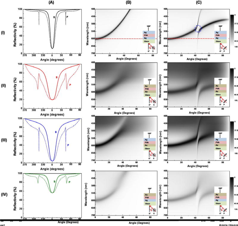
(A) Calculated angle-dependent reflectivity for MDM substrates (I–IV) with 600 nm incident light. (B) Reflectivity dispersion diagrams, R(λ, θ), for S-polarized illumination for substrates (I–IV). (C) Reflectivity dispersion diagrams for P-polarized illumination for substrates (I–IV); reflectivity scale from 0 to 100%. Insets in B and C show the MDM structure, illumination geometry and polarization. PVA thickness for substrate I: 150 nm, Substrate II: 135 nm, Substrates III and IV: 142 nm.
The complete dispersion plots, R(λ, θ), for this MDM substrate (I), for S- and P-polarized incident light are shown, panels B and C, respectively. The dark shades in these figures represent a decrease in reflectivity and hence indicate the presence of an optical mode. The width and darkness of the shaded area indicates the width and strength of the optical mode. The dispersion plots for S- and P-polarized incident lights are considerably different, suggesting polarization selectivity of the MDM structures. The wavelength of our interest, 600 nm (corresponding to the emission maximum of S101), is marked by a red horizontal line in these diagrams; Figure 2(I: B and C).
For S-polarized light, no optical modes can be observed for light having wavelengths above 600 nm. This suggests that the MDM substrate I, will not allow any coupled S-polarized emission above 600 nm. The R(λ, θ) diagram shows that the resonance wavelength, that is the wavelength where a dip appears in the reflectivity spectrum, is blue-shifted with increase in the incidence angle, giving rise to a hyperbolic dark curve. The curve intersects the Y-axis at 600 nm, corresponding with the resonance of this wavelength at 0°. The hyperbolic-nature of the curve is reminiscent of the Tamm modes observed in the hybrid structures consisting of a metal layer and a truncated 1DPC.14 Tamm states have also been proposed in periodic structures created by alternating metal and dielectric layers.18 Durach and Rusina have recently carried out theoretical calculations on a novel photonic structure composed of metal nanolayer-Bragg mirror-metal nanolayer geometry.19 They have concluded that these structures support resonances that are transitional between Fabry-Pérot and Tamm modes. When the dielectric thickness is larger than the wavelength or the dielectric contrast of the Bragg mirror is removed (which mimics the situation in the present MDM substrates), these modes are conventional Fabry-Pérot resonances, whereas at high dielectric contrast, they transform to Tamm modes.
The dispersion curve for MDM structure I, with P-polarized incident light, also shows a blue-shift of the resonance wavelength with increase in the angle of incidence away from the normal. However, the curve is flatter as compared to that for S-polarized incident light. In addition, a second sharper resonance curve appears for incidence angles exceeding the critical angle of the glass/air interface (41.8°), indicating the presence of another optical mode (discussed later). For 600 nm light, this mode leads to the sharp dip at 44° (and 316° due to symmetry) in the reflectivity plot for P-polarized light (panel A). The coupling between the two P-polarized optical modes leads to a repulsion of the resonances, marked by a blue circle in the dispersion diagram.
From the dispersion diagrams of the other MDM substrates (II–IV), a qualitatively similar picture emerges, as discussed above for structure I. However, differences are observed in the amplitude and width of the resonances. For MDM substrates having Au as the first layer on the glass side (II and III), the dispersion plots appear darker (i.e. lower reflectivity) below ~500 nm; Figure 2(II: B, C) and Figure 2(III: B, C). This is due to the inter-band transitions of Au and the absorption of light in the Au layer. On the other hand, for the Au-PVA-Ag-glass substrate (IV), the reflectivity dips are lower and hence the dispersion plot appears to be weaker; Figure 2(IV: A, B, C). The reflectivities are thus dependent on the specific optical properties of Au and Ag and the metal layer adjacent to the glass side. It is also found that slightly different PVA thicknesses are required for each MDM substrate to obtain the reflectivity dip for 600 nm light at 0° (both S- and P-polarized). Thus, for the Au-PVA-Au-glass substrate (II), the reflectivity dip at 0° (for 600 nm) is obtained with a PVA thickness of 135 nm whereas for the mixed metal substrates (III and IV) the required PVA thickness is 142 nm. The R(λ, θ) plots depicted in Figure 2 for substrates II, III (and IV) correspond to PVA thicknesses of 135 and 142 nm, respectively.
To have a better idea about the nature of the various optical modes that are present in the MDM substrates, we examined the corresponding electric field intensities in the substrates by setting the incident angles and polarizations at the respective resonance positions. Figure 3 shows the electric field intensities (E2) in the MDM substrates I–IV, for 600 nm light (S- and P-polarized) at normal incidence. For all the substrates, the electric field for both polarizations is located in the dielectric layer (PVA) or cavity between the metal films. Any emission that arises due to coupling with this optical mode is referred as cavity-mode-coupled emission (CMCE).20 The field distribution for this optical mode inside the MDM substrate is similar to that of a Tamm state. We make this comparison because the energy is localized below the top metal film. In contrast to surface plasmons, Tamm plasmons (TPs) display unique properties that can offer several advantages. Unlike surface plasmons that can only be created by P-polarized light incident through a prism or grating coupler at the characteristic surface plasmon resonance angle, TPs can be created with incident light normal to the substrate, using both S- and P-polarized light and without the aid of prisms or gratings.14 In this case, the usual Bragg grating in a Tamm structure is replaced by the lower metal film. The field intensities depend on the nature of the metal layers; the highest intensities being obtained for substrate I (Ag-PVA-Ag-glass).
Figure 3.
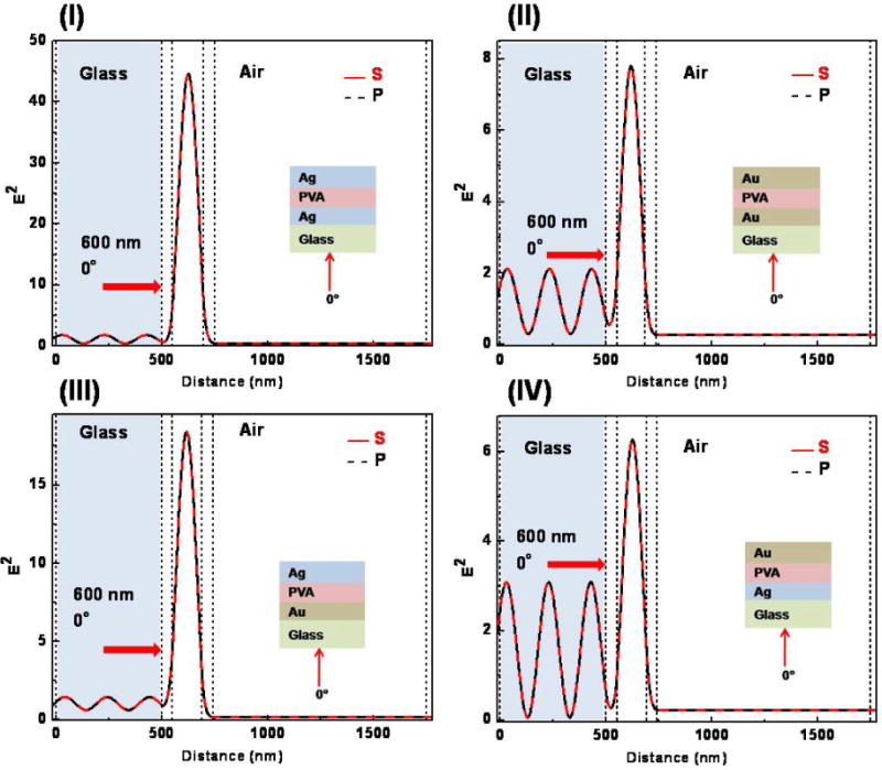
Calculated electric field intensities in different MDM substrates (I–IV) for 600 nm illumination at 0°; S-polarized (red) and P-polarized (black).
We now consider the electric field intensities in the substrates with incident light at angles above the critical angle of the glass/air interface. Figure 4 depicts the electric field intensities in the MDM substrates, I and III (the field intensities for the other substrates are presented in Figure S1, Supporting Information, SI) for P-polarized 600 nm light at the respective resonance position (44°) that is observed in the reflectivity plots (Figure 2, I: A and III: A). For this optical mode, the field is located at the top metal/air interface. Based on the location of the electric field and its polarization (P-polarized), this optical mode can be assigned as the surface-plasmon mode. Typically, when a thin metal film is illuminated by light through a glass prism, the reflectivity is very high except at a specific angle called the surface-plasmon angle (θsp), beyond the critical angle of the system. This reflectivity dip arises due to the excitation of surface-plasmons on the metal/air interface. Excitation of surface plasmons depends on the polarization of the light and the surface-plasmon angle varies with the wavelength of light. S-polarized light cannot create surface-plasmons nor can light incident from the air side. The emission from a fluorophore placed in the vicinity of the metal film, however, can excite and couple with the surface-plasmons due to near-field interactions. So any emission that appears by coupling with this optical mode is called surface-plasmon-coupled emission (SPCE).2 It is now clear that the different optical modes that appear in the reflectivity simulations and dispersion diagrams for the MDM substrates (Figure 2) are the S- and P-polarized cavity modes and the P-polarized surface-plasmon mode (above the critical angle of the glass/air interface). The P-polarized cavity mode and surface-plasmon mode cannot be excited independently at a given angle of incidence or wavelength. The coupling between the P-polarized electromagnetic wave localized at the metal/PVA interface and the mode localized at the metal/air interface leads to the repulsion that is observed in Figure 2(I–IV: C).21 For S-polarized light surface-plasmon propagation is forbidden and only the cavity mode is excited.
Figure 4.
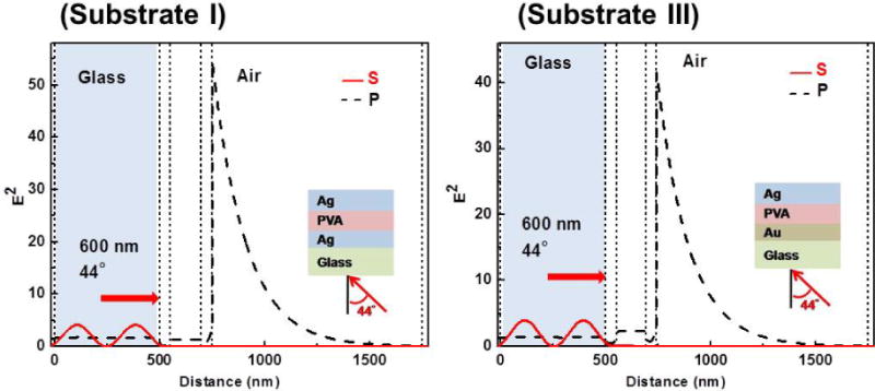
Calculated electric field intensities in MDM substrate I and III for 600 nm illumination at 44°; S-polarized (red) and P-polarized (black). Corresponding electric field distributions for the substrates II and IV are shown in Figure S1, SI.
Based on the above transfer matrix simulations and discussion about the optical modes present in the MDM substrates it is now easier to interpret and analyze the experimentally observed angular emission patterns of the dye, S101 in these substrates, I–IV (Figure 5). In accordance with the reflectivity simulations, the emission at 600 nm appears normal to the glass substrate in each case. However, depending on the metal layers, differences are observed in the width of the angular distribution of emission as well as in the emission intensities. The angular divergence is lowest in the Ag-PVA-Ag-glass substrate (FWHM ~16°) and higher in all the other substrates (~18–22°). This difference in angular distribution may be a result of the larger losses and wider resonances on Au as compared to Ag.
Figure 5.
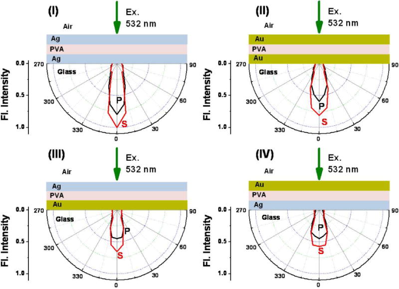
Angle-dependent S- (red) and P-polarized (black) emission intensities at 600 nm from S101 embedded in the PVA layer in MDM substrates (I–IV). The intensities have been normalized with respect to the maximum intensity observed for substrate I.
To interpret the experimentally observed emission intensities, a comparison among all the MDM substrates (I–IV) is difficult because excitation of the dye takes place by illumination through the top metal layer. Since each metal layer attenuates the excitation energy to a different extent (extinction spectra of Ag and Au metal films are presented in Figure S2, SI), the effective excitation intensity of the dye is not similar for the MDM substrates having different metals as the top layer. So to analyze the observed emission intensities from S101 in MDM substrates, we have qualitatively compared the intensities between substrates having the same metal as the top layer. Comparing between substrate I and III (both having Ag as the top layer) it is seen that the emission intensity from S101 embedded in structure I is greater than that in structure III. Similarly, comparing substrate II and IV (both having Au as the top layer), the emission intensity observed from the dye embedded in structure II is greater than that of IV. The origin of this difference can be attributed to the magnitude of the electric fields in the respective MDM structures. Figure 4 shows the trend in the electric field intensities that is, E2(I) > E2(III) and E2(II) > E2(IV). As the emission from S101 arises due to coupling with the optical modes, it is quite logical that the substrate having higher electric fields leads to higher emission intensities.
Although, reflectivity simulations suggest similar intensities for S- and P-polarized emission in each MDM substrates, the experimentally observed intensity for S-polarized emission is higher than P-polarized emission in all the cases (Figure 5). Previous studies indicate that the excitation and/or emission of probes coupled with optical modes depend on orientation of the transition dipoles relative to the sample plane. It has been observed before that for S-polarized excitation, S-polarized emission intensities are higher than P-polarized emission intensities, while for P-polarized excitation, P-polarized emission intensities are higher.15,24 In the present experiments, the excitation source was vertically polarized (Figure 1). Hence, the S-polarized emission intensities appear to be higher than P-polarized emission intensities in Figure 5.
An interesting deviation is observed between the experimentally observed angular emission patterns and that expected from the reflectivity calculations. According to the reflectivity simulations, P-polarized emission should be observed from S101 at angles greater than the critical angle of the glass/air interface (due to coupling with surface-plasmon mode), in addition to the emission observed at 0° (due to coupling with cavity mode). However, the CMCE is the most prominent emission in all the MDM substrates. The SPCE emission is very weak and almost undetected in the experimentally observed emission patterns. This difference between the calculated and observed emission can be explained by considering the location of the dye and the location of the electric fields for each mode in the MDM substrates. The cavity mode is localized in the dielectric medium between the metal films. Since the dye is present in the same region, the near-field coupling of the emission with the cavity mode is expected to be very efficient. This leads to intense CMCE. On the other hand, the electric field maxima for the surface-plasmon mode are located above the top metal film (Figure 4). As a result, the coupling efficiency with the dye molecules located within the PVA layer is expected to be weaker.
According to the above proposition, strong SPCE may be anticipated for dye molecules located on the top metal layer surface. To determine the effect of dye location on the coupling efficiency, we carried out emission measurements with dye molecules positioned on the top metal film. The angular emission pattern for such a system is illustrated in Figure 6. In contrast to the previous observation (Figure 5(I)), the emission in this case is found to be predominantly directed through the surface-plasmon mode, leading to strong P-polarized SPCE. The coupling with the cavity mode is inefficient, hence the CMCE that is observed normal to the substrate (0°), is weaker. This result is very interesting and emphasizes the role of dye location in the near-field coupling of the emission with the existing optical modes in the MDM substrate. To the best of our knowledge this is the first report of coupled emission across a MDM structure. Previous reports discussed only emission from probes within the central dielectric layer.22–23 The appearance of CMCE and SPCE at different angles in the MDM substrates could be useful in designing fluorescence assays based on monitoring the mode coupled fluorescence intensities at two different observation angles.
Figure 6.
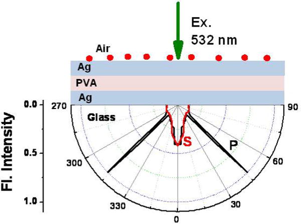
Angle-dependent S- (red) and P-polarized (black) emission intensities at 600 nm from S101 placed on the top metal layer in the MDM substrate I.
It is informative to compare the dispersion diagrams, electric field intensity distributions and experimentally observed angular emission patterns in MDM substrates with those in the MD substrates, without the top metal film, as depicted in Figure 7 (and Figure S3, SI). In the latter case (PVA-Ag-glass), only S-polarized emission can be observed (at 600 nm) at an angle of 45° from the normal. No beaming emission is seen perpendicular to the substrate. This observation is in accordance with the reflectivity calculations and the R(λ, θ) dispersion plots. The dark curve of low reflectance is observed only with S-polarized light and it does not intersect the Y-axis at 600 nm (Figure 7A). The electric field intensity maximum for the MD substrate lies in the PVA layer adjacent to the metal film and exists only for S-polarized light at the corresponding resonance wavelength and angle. The electric field distribution resembles that of guided modes. Hence, the emission from S101 that is observed by coupling with this optical mode can be assigned as guided-mode-coupled emission. Emission at several different angles, having both S- and P-polarization has been reported previously for dye molecules placed on thick dielectric layers above a metal film, due to the presence of waveguide modes.24
Figure 7.
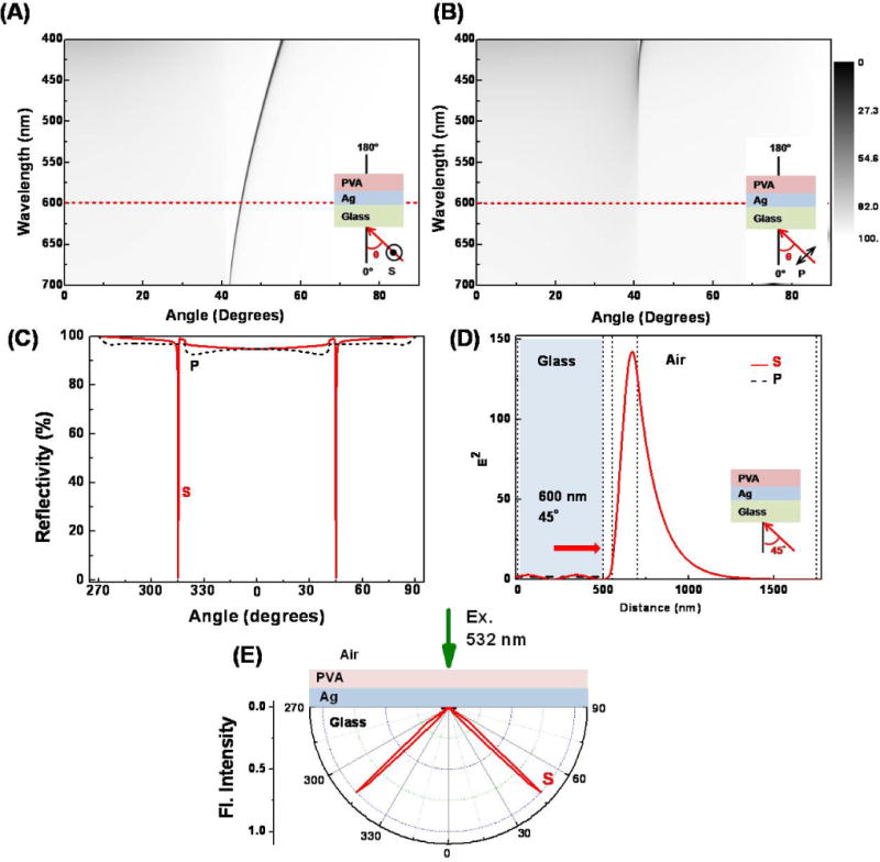
Calculated reflectivity dispersion diagrams, R(λ, θ), for (A) S-polarized and (B) P-polarized illumination in the PVA-Ag-glass MD substrate; (C) angle-dependent reflectivity with 600 nm incident light; (D) electric field intensity for 600 nm illumination (S- and P-polarized) at the reflectivity minimum of 45° and (E) experimentally observed angle-dependent emission intensities at 600 nm from S101 embedded in the PVA layer, PVA thickness 150 nm.
Since for the MDM substrates I–IV, the reflectivity dip for 600 nm light was obtained normal to the surface (0°) at different thicknesses of the PVA layer, we used simulations to examine the variation in the resonance wavelength of the substrates with the thicknesses of the dielectric layer. Figure 8A shows that the resonance wavelength (for reflectivity dip at 0°) for all the substrates decreases with increase in the PVA thickness and at a particular PVA thickness the resonance wavelength depends on the metal layer composition of the MDM substrate. As discussed before, the resonance wavelength corresponds to the excitation of an optical mode in the MDM substrate and the coupled emission in turn follows the properties of this mode. So the horizontal line at 600 nm in Figure 8A basically indicates the PVA thickness requirement for obtaining beaming emission from S101 in each MDM substrate. The difference among the various MDM substrates is attributed to the characteristic optical properties of Ag and Au. The dependence of the resonance wavelength on the metallic composition of the MDM substrate is illustrated more clearly in Figure 8B (and Figure S4, SI). Thus, at a PVA thickness of 135 nm (marked by a vertical line in Figure 8A), the wavelength for beaming emission is found to be 557 nm for MDM substrate I, 600 nm for substrate II and 580 nm for substrates III and IV. This is an interesting result which suggests that the type of metal in the MDM substrate can alter the color of the emission wavelength. If the PVA layer contains a mixture of dyes or an active material that emits over a broad wavelength range, the MDM substrates can be used to extract different wavelengths normal to the substrate, by choosing different metal layers or different dielectric thicknesses.
Figure 8.
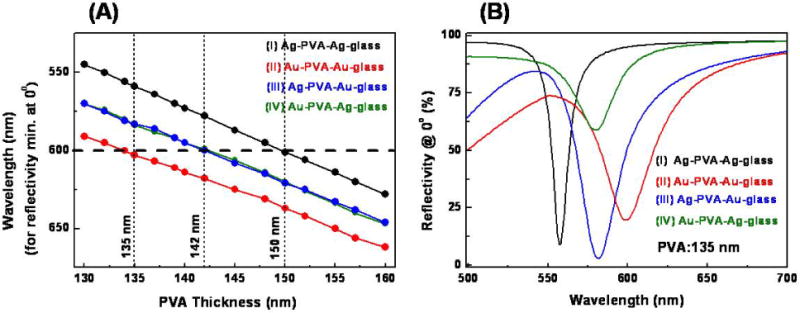
(A) Variation of the beaming wavelength (observed normal to the substrate at 0°) with PVA thickness in different MDM substrates. The wavelength of interest in the present study (600 nm) is shown by a dashed horizontal line. (B) Wavelengths at which the reflectivity dip at 0° is obtained in different MDM substrates for a particular PVA thickness (135 nm).
From another perspective, we examined the effect of different PVA thicknesses and different metal layers in the MDM substrates, on the angular dependence of the coupled emission at a fixed wavelength of 600 nm. As mentioned before, the coupled emission essentially carries the properties of the optical modes. So the spectral and spatial properties of the emission can be derived based on reflectivity simulations. For example, if the reflectivity minimum for 600 nm light is observed at a particular angle, θ°, from the surface normal of the MDM substrate, the emission at 600 nm will also appear at the same angle of θ°. The results from several reflectivity simulations with 600 nm incident light for the MDM substrates (I–IV) are summarized in Figure 9A. From this figure it is inferred that the angular variation of the surface-plasmon mode and hence the P-polarized SPCE, is very weakly dependent on the PVA thickness. However, the angular dependence of CMCE is not only sensitive to the PVA thickness but is also different for S- and P-polarized emissions in each MDM substrate. The difference in the observation angle for S- and P-polarized CMCE at a particular PVA thickness increases with increase in the PVA thickness. This result is quite significant and suggests that MDM substrates with varying dielectric thickness can be used to obtain polarization-resolved emission at different observation angles. For example, for the MDM substrate I, emission at 600 nm would be observed at three different angles when the PVA thickness is 155 nm. The emission observed at 17° and 44° will be P-polarized while the emission at 12° will be S-polarized. The reflectivity plots with 600 nm light and electric field intensity distributions at the characteristic resonance angles for this substrate are depicted in Figures 9B–E.
Figure 9.
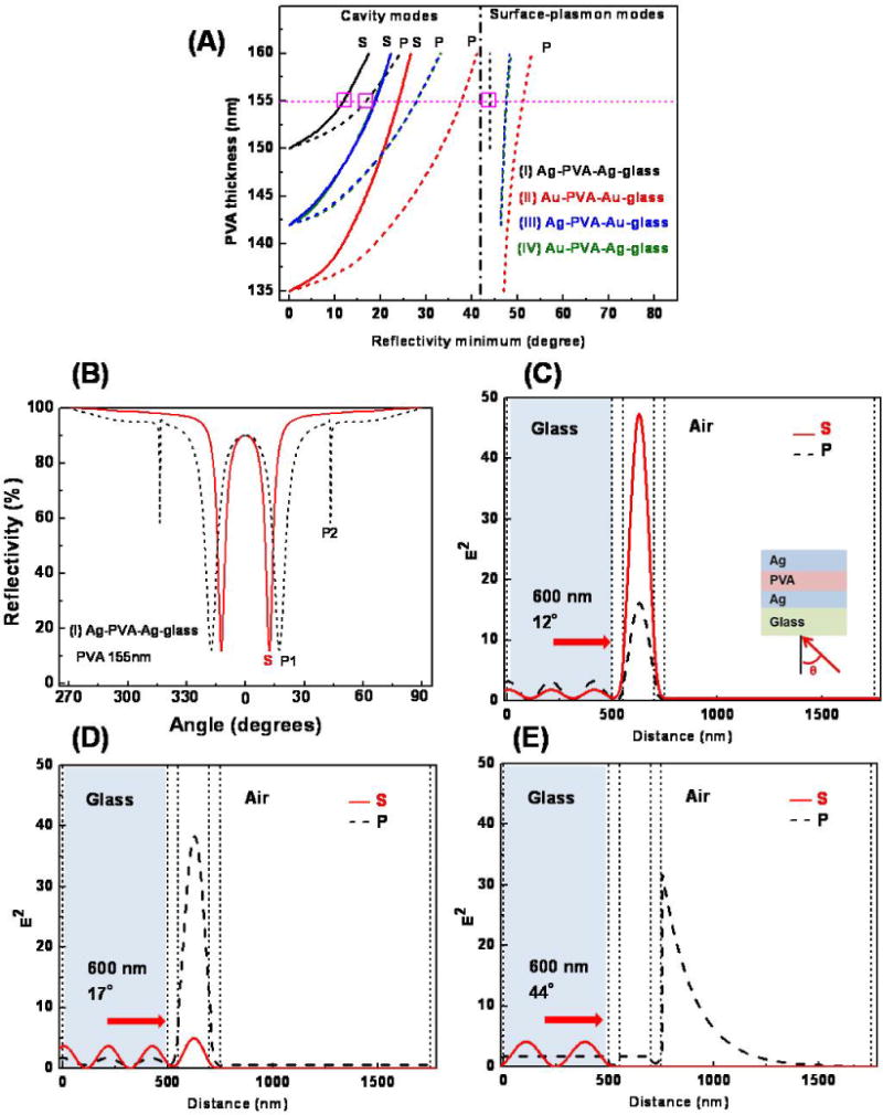
(A) Angular dependence of the reflectivity minima on the PVA thickness in MDM substrates I–IV, plots for substrate III and IV are similar and superimposed. (B) Angle-dependent reflectivity for Ag-PVA-Ag-glass MDM substrate with PVA thickness of 155 nm. (C–E) Electric field intensities in the Ag-PVA-Ag-glass substrate with PVA thickness of 155 nm for each resonance angle (shown by horizontal line in A). All calculations have been performed for 600 nm (S- and P-polarized).
Controlling the emission from active materials such as dye molecules, luminescent nanomaterials or quantum dots is an important area of research with widespread applications, and MDM structures can offer several opportunities for controlling luminescence in nanoscale dimensions. The MDM structures display useful color tunability, wavelength selectivity by suppressing longer wavelength emissions where optical modes do not exist and polarization separability based on observation angle. All of these features are valuable for future fluorescence applications, display technologies and in light emitting devices. Importantly, MDM structures can provide directional emission close to the surface normal. This can largely simplify the use of surface-coupled emission for applications such as microscopy, microarrays and portable diagnostic devices. The present study will be useful for designing and interpreting the emission from dye molecules in MDM substrates and for conceptualizing different approaches for fluorescence based applications.
Conclusion
The use of MDM structures to manipulate fluorescence requires a basic understanding of the factors that affect the coupling efficiency of emission from dye molecules and the spectral and spatial distribution of the coupled emission. The present study shows that the symmetric MDM substrate Ag-PVA-Ag-glass provides the best emission intensities for CMCE, perpendicular to the substrate and with narrow angular divergence. The simple MDM substrates allow direct excitation and emission of both P- and S-polarized light, normal to the surface. They can be readily introduced into existing instruments, for microscopy and microarray applications. The location of the dye in the MDM substrate determines the nature of the coupled emission. For dye molecules placed within the dielectric layer in the MDM substrates, the observed emission is essentially CMCE due to coupling with the cavity mode. For dye molecules placed on the top metal surface, the observed emission is predominantly SPCE, due to efficient coupling with the surface-plasmon mode. This work also reveals the importance of the metal layers and dielectric thickness in controlling the wavelength, angular dependence and polarization of the emission. These features can be valuable for future display applications.
Supplementary Material
Acknowledgments
SDC acknowledges financial support from SERB Women Excellence Award Grant, SB/WEA-010/2013, and the support and encouragement from the host institute. This work was also supported by NIH Grants GM107986, EB006521 and AI087968.
References
- 1.Lakowicz JR, Shena Y, D’Auria S, Malicka J, Fang J, Gryczynski Z, Gryczynski I. Radiative decay engineering: 2. Effects of silver island films on fluorescence intensity, lifetimes, and resonance energy transfer. Anal Biochem. 2002;301:261–267. doi: 10.1006/abio.2001.5503. [DOI] [PMC free article] [PubMed] [Google Scholar]
- 2.Lakowicz JR. Radiative Decay Engineering 3. Surface Plasmon-Coupled Directional Emission. Anal Biochem. 2004;324:153–169. doi: 10.1016/j.ab.2003.09.039. [DOI] [PMC free article] [PubMed] [Google Scholar]
- 3.Gryczynski I, Malicka J, Gryczynski Z, Lakowicz JR. Radiative Decay Engineering 4. Experimental Studies of Surface Plasmon-Coupled Directional Emission. Anal Biochem. 2004;324:170–182. doi: 10.1016/j.ab.2003.09.036. [DOI] [PMC free article] [PubMed] [Google Scholar]
- 4.Gryczynski I, Malicka J, Gryczynski Z, Lakowicz JR. Surface Plasmon-Coupled Emission with Gold Films. J Phys Chem B. 2004;108:12568–12574. doi: 10.1021/jp040221h. [DOI] [PMC free article] [PubMed] [Google Scholar]
- 5.Enderlein J, Ruckstuhl T. The Efficiency of Surface-Plasmon Coupled Emission for Sensitive Fluorescence Detection. Optics Express. 2005;13:8855–8865. doi: 10.1364/opex.13.008855. [DOI] [PubMed] [Google Scholar]
- 6.Gryczynski Z, Borejdo J, Calander N, Matveeva EG, Gryczynski I. Minimization of Detection Volume by Surface-Plasmon-Coupled Emission. Anal Biochem. 2006;356:125–131. doi: 10.1016/j.ab.2006.05.007. [DOI] [PubMed] [Google Scholar]
- 7.Xie TT, Liu Q, Cai WP, Chen Z, Li YQ. Surface Plasmon-Coupled Directional Emission Based on a Conformational-Switching Signaling Aptamer. Chem Commun. 2009:3190–3192. doi: 10.1039/b823352g. [DOI] [PubMed] [Google Scholar]
- 8.Yuk JS, McDonagh C, MacCraith BD. Demonstration Of A Surface Plasmon-Coupled Emission (Spce)-Based Immunoassay in the Absence of a Spacer Layer. Anal Bioanal Chem. 2010;398:1947–1954. doi: 10.1007/s00216-010-4026-8. [DOI] [PubMed] [Google Scholar]
- 9.Yuk JS, Trnavsky M, McDonagh C, MacCraith BD. Surface Plasmon-Coupled Emission (Spce)-Based Immunoassay Using a Novel Paraboloid Array Biochip. Biosensors and Bioelectronics. 2010;25:1344–1349. doi: 10.1016/j.bios.2009.10.026. [DOI] [PubMed] [Google Scholar]
- 10.Dutta Choudhury S, Badugu R, Nowaczyk K, Ray K, Lakowicz JR. Tuning Fluorescence Direction with Plasmonic Metal–Dielectric–Metal Substrates. J Phys Chem Lett. 2013;4:227–232. doi: 10.1021/jz301867b. [DOI] [PMC free article] [PubMed] [Google Scholar]
- 11.Dutta Choudhury S, Badugu R, Ray K, Lakowicz JR. Steering Fluorescence Emission with Metal-Dielectric-Metal Structures of Au, Ag, and Al. J Phys Chem C. 2013;117:15798–15807. doi: 10.1021/jp4051066. [DOI] [PMC free article] [PubMed] [Google Scholar]
- 12.Becker H, Friend RH, Wilkinson TD. Light Emission from Wavelength-Tunable Microcavities. Appl Phys Lett. 1998;72:1266–1268. [Google Scholar]
- 13.Becker H, Burns SE, Tessler N, Friend RH. Role of Optical Properties of Metallic Mirrors in Microcavity Structures. J Appl Phys. 1997;81:2825–2829. [Google Scholar]
- 14.Badugu R, Descrovi E, Lakowicz JR. Radiative Decay Engineering 7: Tamm State-Coupled Emission Using a Hybrid Plasmonic–Photonic Structure. Anal Biochem. 2014;445:1–13. doi: 10.1016/j.ab.2013.10.009. [DOI] [PMC free article] [PubMed] [Google Scholar]
- 15.Badugu R, Lakowicz JR. Tamm State-Coupled Emission: Effect of Probe Location and Emission Wavelength. J Phys Chem C. 2014;118:21558–21571. doi: 10.1021/jp506190h. [DOI] [PMC free article] [PubMed] [Google Scholar]
- 16.Kavokin AV, Shelykh A, Malpuech G. Lossless Interface Modes at the Boundary between Two Periodic Dielectric Structures. Phys Rev B. 2005;72:233102(1–4). [Google Scholar]
- 17.Kaliteevski M, Iorsh I, Brand S, Abram RA, Chamberlain JM, Kavokin AV, Shelykh IA. Tamm Plasmon-Polaritons: Possible Electromagnetic States at the Interface of a Metal and a Dielectric Bragg Mirror. Phys Rev B. 2007;76:165415(1–5). [Google Scholar]
- 18.Vukovic SM. Plasmonic Bragg Reflector and Tamm Plasmon Polaritons in Metal–Dielectric Superlattices. Acta Physica Polonica A. 2009;119:678–680. [Google Scholar]
- 19.Durach M, Rusina A. Transforming Fabry-Pérot Resonances into a Tamm Mode. Phys Rev B. 2012;86:235312(1–6). [Google Scholar]
- 20.Zhang D, Badugu R, Chen Y, Yu S, Yao P, Wang P, Ming H, Lakowicz JR. Back Focal Plane Imaging Of Directional Emission from Dye Molecules Coupled to One-Dimensional Photonic Crystals. Nanotechnology. 2014;25:145202(1–10). doi: 10.1088/0957-4484/25/14/145202. [DOI] [PMC free article] [PubMed] [Google Scholar]
- 21.Afinogenov BI, Bessonov VO, Nikulin AA, Fedyanin AA. Observation of Hybrid State of Tamm and Surface Plasmon-Polaritons in One-Dimensional Photonic Crystals. Appl Phys Lett. 2013;103:061112(1–6). [Google Scholar]
- 22.Liu JSQ, Brongersma ML. Omnidirectional Light Emission via Surface Plasmon Polaritons. Appl Phys Lett. 2007;90:091116(1–3). [Google Scholar]
- 23.Feng J, Okamoto T, Simonen J, Kawata S. Color-Tunable Electroluminescence from White Organic Light-Emitting Devices through Coupled Surface Plasmons. Appl Phys Lett. 2007;90:081106(1–3). [Google Scholar]
- 24.Gryczynski I, Malicka J, Nowaczyk K, Gryczynski Z, Lakowicz JR. Effects of Sample Thickness on the Optical Properties of Surface Plasmon-Coupled Emission. J Phys Chem B. 2004;108:12073–12083. doi: 10.1021/jp0312619. [DOI] [PMC free article] [PubMed] [Google Scholar]
Associated Data
This section collects any data citations, data availability statements, or supplementary materials included in this article.


