Abstract
The lock-in amplifier is a critical component in many different types of experiments, because of its ability to reduce spurious or environmental noise components by restricting detection to a single frequency and phase. One example application is pump-probe microscopy, a multiphoton technique that leverages excited-state dynamics for imaging contrast. With this application in mind, we present here the design and implementation of a high-speed lock-in amplifier on the field-programmable gate array (FPGA) coprocessor of a data acquisition board. The most important advantage is the inherent ability to filter signals based on more complex modulation patterns. As an example, we use the flexibility of the FPGA approach to enable a novel pump-probe detection scheme based on spread-spectrum communications techniques.
I. INTRODUCTION
Lock-in amplifiers (also known as phase-sensitive detectors) enable detection and measurement of small ac signals in the presence of overwhelming noise. These instruments are used in a variety of optical measurements and are especially critical in nonlinear and ultrafast optics laboratories. Implementing a lock-in amplifier with digital signal processing (DSP) techniques enables flexibility, application-specific customizations, and novel detection techniques—innovations that go beyond mere improvements in speed and signal-to-noise ratio (SNR).1–3 Increasingly, DSP lock-ins are being developed on field-programmable gate array (FPGA) hardware instead of DSP microprocessors,1–3 in order to benefit from increased performance.4 Here, we present a digital lock-in implemented on the coprocessor FPGA of a high-speed data acquisition board, tailored to the requirements of nonlinear optical microscopy (i.e., multiphoton microscopy). The most important advantage is the inherent ability to filter based on more complex modulations. We also demonstrate a novel detection scheme for time-resolved optical spectroscopy based on spread-spectrum communication techniques.5,6
In recent years, a number of advanced microscopy techniques have emerged on the basis of detecting nonlinear optical interactions in biological tissue.7,8 Examples include multiphoton-excited fluorescence, second- and third-harmonic generation, coherent anti-Stokes Raman scattering (CARS), stimulated Raman scattering (SRS), instantaneous and time-delayed optical Kerr effect, photothermal heterodyne mixing, and transient absorption (i.e., pump-probe). The challenges in implementing these come from the need to maximize both speed and sensitivity, in order to mitigate optical damage and sample larger volumes of tissue. Potential tissue damage from both peak power and average power is a cause for concern;9 often, the safe deliverable power is far below what the laser can produce. In addition, most tissue imaging applications put a high premium on acquisition speed, to adequately sample the tissue volume in a reasonable time. This is especially important in cancer applications, and inadequate spatial sampling of the intrinsic heterogeneity can lead to misdiagnosis and underestimation of tumor aggressiveness.10
Multiphoton microscopy techniques may be divided into two categories, based on the way in which the nonlinear interaction generates a detectable signal. Those that emit light at wavelengths that are distinct from the incident laser—fluorescence, harmonic generation, and CARS—are readily detected with an optical filter and a sensitive photodetector (such as a photomultiplier tube (PMT)). However, non-emissive interactions (which often give completely different and useful contrast) must be detected via their perturbations to the incident light fields. In biological matter, these perturbations are small (on order of <10−5, limited by the multiphoton ionization and thermal damage considerations mentioned above) and are easily overwhelmed by noise such as laser intensity fluctuations and Johnson noise. These perturbations may be detected interferometrically,11–13 but the most common approach is to modulate the pump beam and filter the detected probe signal with a lock-in amplifier synchronized to the pump modulation. Lock-in amplifiers can also be used to measure lifetimes of other transient optical phenomena such as fluorescence and phosphorescence decay.
The requirements of lock-in amplifiers for multiphoton imaging applications are unique, in that speed is more important than phase accuracy. In order to mitigate 1/f noise and be fast enough to permit imaging with reasonable frame rates, the lock-in must be able to detect modulations >1 MHz and have integration times <100 μs. Though suitable commercial instruments are available (e.g., from Signal Recovery, Stanford Research Systems, and Zurich Instruments), there has been growing interest lately in custom-built hardware for multiphoton imaging. For example, Saar et al. fabricated an analog lock-in to achieve video rate (25 frames/s) SRS imaging for in vivo applications.14 Other approaches forego the lock-in amplifier altogether by placing a resonant LC circuit in the photodiode amplifier,15 performing collinear balanced detection,16 or directly digitizing the photodiode signal, performing lock-in demodulation and further post-processing in software.17
In this work, we have replaced the lock-in amplifier with a high-speed data acquisition board, performing all signal processing in the coprocessor FPGA. This approach is extremely flexible, as all aspects of the signal processing pipeline can be modified by editing the source code, recompiling, and downloading to the FPGA. This approach also has an advantage over analog hardware, in that the source code and/or compiled binaries can be shared electronically and downloaded to the target FPGA board—there is no need to fabricate new circuit boards, place, and solder components, etc. In this article, we first present details of the design and implementation, followed by two applications. The first is the basic single-frequency lock-in demodulation with an in vivo imaging application. The second goes beyond the capability of single-frequency lock-in amplifiers by using a spread-spectrum approach for characterizing long-time (μs) dynamics.
II. DIRECT NARROW-BAND LOCK-IN DETECTION BY DIGITAL SIGNAL PROCESSING
A. Optical setup
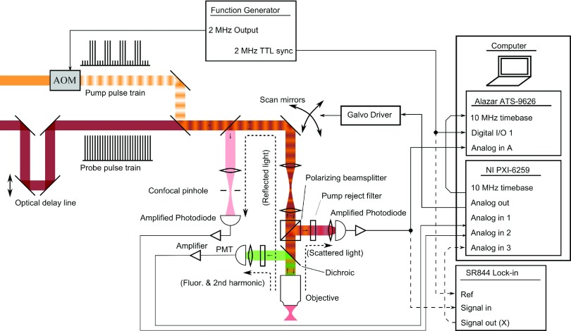
The experiments described here are performed on a custom-built laser scanning microscope, as depicted in Figure 1. Pump and probe pulses are generated by a Chameleon femtosecond oscillator (Coherent, Santa Clara, CA, USA) and a Mira optical parametric oscillator (Coherent). The pump is modulated by an acousto-optic modulator (AOM), then combined with the probe by a dichroic mirror, and directed into the microscope. For multiphoton fluorescence/SHG and confocal imaging, a data acquisition board (NI PXI-6259, National Instruments, Austin, TX) is used both for collecting data and controlling the galvanometric scan mirrors. Pump-probe signal is collected with a polarizing beamsplitter and photodiode and digitized by an ATS-9626 high-speed data acquisition board (AlazarTech, Pointe-Claire, QC, Canada). All DSP operations are performed in the coprocessor FPGA of the ATS-9626. The two data acquisition boards are synchronized with a common 10 MHz timebase. Alternatively, a commercial lock-in amplifier (SR844, Stanford Research Systems, Sunnyvale, CA, USA) is used for comparison.
FIG. 1.
Optical setup and electronics layout for nonlinear optical microscope including detection channels for confocal reflectance, multiphoton fluorescence, and pump-probe. Galvo scanners are controlled by the analog output of the NI PXI-6259 card. Confocal reflectance and multiphoton fluorescence signals are captured by the NI PXI-6259 analog inputs. Pump-probe detection is accomplished through either the SR844 lock-in or the custom FPGA firmware loaded on to the Alazar ATS-9626.
B. Design and implementation of FPGA-based lock-in amplifier
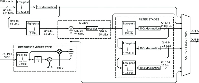
Figure 2 shows a block diagram of the lock-in amplifier. A brief overview follows; for more detail, see the Appendix. After digitization at 250 MS/s, the 16-bit input is downsampled to 25 MS/s, filtered to remove the DC offset, and directed to the mixer, where it is multiplied by the reference. The reference waveform is derived from a digital (square wave) synchronization signal in a few steps. A narrowband filter isolates the fundamental component of the square wave, which is differentiated to produce the quadrature component. These two components are summed in appropriate proportion to produce the reference sinusoid with the desired phase shift. This is then multiplied by the input signal in the mixer. Mixer output gain is controlled at this point by selecting a 16-bit slice from the 32-bit product to pass on to the low-pass filter stages. Three successive low-pass filter stages, each with 100 × downsampling, produce final output rates of 250 kS/s, 2.5 kS/s, and 25 S/s, which are selected by the output multiplexer (MUX). Filters are implemented as multi-stage finite impulse response (FIR) in order to conserve resources (see the Appendix). Other signals, such as the phase-shifted reference wave or the mixer output, can be optionally selected by the MUX. The output of the MUX is passed to the data acquisition board’s main FPGA, cached in the on-board memory, and retrieved by the microscope control software through the peripheral component interface (PCI) bus.
FIG. 2.
Block diagram schematic of FPGA-based lock-in amplifier. Fixed-point datapath widths specified in Qn.m format (see the Appendix).
C. Results
1. 2-photon absorption in rhodamine 6G
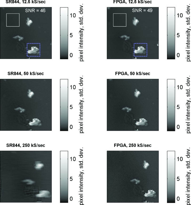
We compare signal to noise performance in a multiphoton imaging application against the SR844 lock-in amplifier, measuring 2-photon absorption at 720/817 nm in rhodamine 6G crystals, for varying pixel sample rates. The SR844 is operated in “no filter” mode (nominal output rate of 48–96 kS/s, depending on operating frequency); its output is captured by the National Instruments data acquisition board (NI-DAQ), running at a 250 kS/s sample rate. The FPGA lock-in is operated in 250 kS/s output mode. Effective pixel rate is varied by changing the number of samples averaged per pixel, e.g., 10 samples/pixel = 25 kS/s. To make a side-by-side comparison, each image is normalized by subtracting the mean pixel value and dividing by the overall standard deviation. The results are shown in Figure 3. Signal to noise ratio is compared for the slowest pixel rate, 12.5 kS/s. Noise is estimated as the standard deviation in a blank region, outlined by the white box, and signal is estimated as the standard deviation in the region outlined with a blue dashed box. Both instruments have comparable SNR at low imaging speeds, but only the FPGA lock-in produces sharp images at high speeds.
FIG. 3.
Comparing speed and SNR between SR844 and FPGA lock-in devices and detecting 2-photon absorption on crystals of rhodamine 6G on a slide. Images with 256 × 256 resolution were acquired at 3 scan rates: 12.5 kS/s (5.2 s/frame), 50 kS/s (1.3 s/frame), and 250 kS/s (0.26 s/frame). Signal and noise estimated from regions indicated with blue dashed box and white box, respectively.
A practical upper limit on imaging speed will depend on several factors. On our microscope, the galvo scanners currently limit pixel rates to 250 kS/s, but the ATS-9626 is capable of acquiring and streaming the full 250 MS/s over the PCI express bus. In our design, all multipliers are pipelined, so that in principle, the output of the mixing step can run at 250 MS/s. From there, the maximum demodulation frequency will be limited to the Nyquist frequency of fmax = 125 MHz, and the maximum output sample rate from the low-pass filtering step will be limited to 125 MS/s, if the initial 10 × decimation step is bypassed. However, the typical 80 MHz Ti:sapphire oscillator employed in multiphoton microscopes will limit fmax to 40 MHz. Note that potential high-speed applications were one of the reasons for using FIR instead of infinite impulse response (IIR) filters (see the Appendix). It should also be noted that there are commercially available high-speed data acquisition/FPGA boards that exceed several GS/s throughput, so much higher speeds can eventually be realized with the approach described here.
2. In vivo pump-probe imaging of melanin
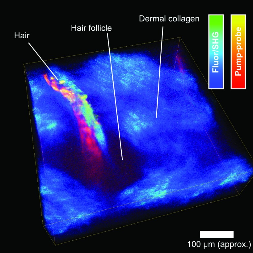
Our primary target application in developing this instrument is for in vivo pump-probe microscopy of pigmented lesions and melanoma. Using the traditional lock-in amplifier, we have been imaging models of human melanoma in mice, in order to characterize changes in melanocyte pigment chemistry during the early stages of tumor formation.18–20 For this application, imaging speed is important because of the limited time window for imaging during anesthesia and the large size of the areas to be sampled. The image shown in Figure 4 is the first in vivo z-stack acquired with the new FPGA-based lock-in amplifier, acquired under a protocol approved by the Institutional Animal Care and Use Committee at Duke University. The subject is a brown-haired mouse (Jackson Labs Strain C57BR/cdJ), under isoflurane anesthesia. The contrast in the pump-probe channel comes from excited state absorption in melanin in the hair.21 Multiphoton fluorescence/SHG is acquired simultaneously with a PMT through the NI-DAQ board, providing complementary structural contrast. The entire 512 × 512 × 150 stack was acquired in less than 3 min—10 × faster than would be possible with the SR844.
FIG. 4.
In vivo image of mouse hair and follicle acquired at 250 kS/s (0.26 s/frame). Fluorescence/SHG and pump-probe images acquired simultaneously. 3D reconstruction rendered from a z-stack using Avizo (FEI, Hillsboro, Oregon, USA).
III. DIRECT-SEQUENCE SPREAD SPECTRUM APPROACH FOR MEASURING LONG-LIVED STATES
In this section, we demonstrate an application that goes beyond the capabilities of a traditional lock-in amplifier. Time-domain measurements of excited-state photodynamics are often measured with low repetition rate lasers, so that the material has time to relax back to a thermal equilibrium state in between repetitions of the pump pulse. In biomedical imaging applications, high repetition rate lasers are employed, trading off pulse energy for more signal averaging; in this scenario, using a pulse picker to reduce repetition rate and allowing for relaxation between pulses would severely limit SNR, because far fewer pulses would be averaged in the measurement period. Here, we employ a spread-spectrum modulation to recover long-lived pump-probe signals directly in the time domain, using a high repetition rate laser.
A. Frequency-domain lifetime measurements with lock-in detection
The most common strategy for measuring lifetimes that exceed the laser repetition rate is to modulate the pulse train at a lower frequency and use a lock-in to determine the frequency-dependent phase response of the system. The detected signal is a convolution of the optical response with the excitation waveform. In the case of a sinusoidally modulated excitation beam and a single-exponential decay,
In the case of a single exponential, the relationship between the modulation frequency f, decay time τ, and the measured phase θ is22
The frequency must be selected near 2πf ≈ 1/τ in order to accurately determine the lifetime from the measured phase. In practice, f is scanned over a range (i.e., swept-spectrum or chirped excitation frequency) and θ is fit to an arctangent to estimate τ. Of course, the above analysis assumes a single-exponential decay behavior. Multi-exponential kinetics can be recovered from these measurements through numerical model fitting.23 Though frequency-domain and time-domain approaches are in principle equivalent, being related to one another by a Fourier transform, there are tradeoffs between the two methods that determine which will be more appropriate to a given measurement scenario.6,24
B. Principle of direct-sequence spread spectrum modulation for measuring excited state dynamics
Here, we implement a spread-spectrum approach to encode the excited state dynamics with a pseudo-random binary sequence, such that the time-resolved kinetics can be directly retrieved from the measured signal. Such an approach to time-resolved luminescence has been proposed and simulated,6 but has not yet to our knowledge been implemented for real-time measurements of optical transients nor has it been applied to pump-probe microscopy. Modern communications devices (e.g., cellular phones and WiFi) encode their transmissions with a broad-band carrier.25,26 One way to do this is to mix the signal with a pseudo-random binary sequence (PRBS); the receiver can only decode the transmission if it can produce a copy of the encoding sequence. This approach, known as direct-sequence spread spectrum (DSSS), makes both eavesdropping and jamming more difficult, but it has another important feature which we shall leverage here. The decoder must not only reproduce the encoding sequence but also match the time delay between the received signal and the sequence precisely. This is because a pseudo-random sequence is non-repetitive and is uncorrelated with time-delayed copies of itself. This autocorrelation property can be used in a pump-probe or phosphorescence lifetime experiment to selectively “tune” specific time delays of the excited state relaxation by varying the electronic delay between the pseudo-random sequence and the measured signal. This we call a time-resolved direct-sequence spread spectrum (TR-DSSS) measurement, and it could have significant advantages for high-speed imaging scenarios where the excited state relaxation is slower than the pixel dwell time, such as phosphorescence lifetime27 and photothermal heterodyne microscopy.28
Similarly to the frequency domain case, the measured signal is a convolution of the PRBS with the optical impulse response h(t),
The signal at a particular electronic time delay Δt is demodulated by multiplication with a time-delayed copy of the PRBS and low-pass filtering (integration),
It can be shown that the measured signal is the optical response convolved with the autocorrelation of the pseudo-random sequence
where ∗ denotes the cross-correlation operator. This enables TR-DSSS to directly resolve decay kinetics by varying the electronic time delay Δt, without requiring a priori knowledge of the optical response h. Note that the instrument response function (IRF) is, by definition, PRBS ∗ PRBS.
C. Implementation and experimental setup
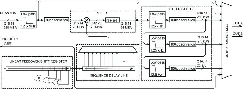
Figure 5 shows a schematic of the TR-DSSS FPGA layout. The main difference between this and the lock-in depicted in Figure 2 is the use of a linear feedback shift register to generate a pseudo-random modulation sequence, which is fed to both an internal delay line preceding the mixer and the digital output port. This sequence is passed to the AOM modulation electronics to impose the pseudo-random sequence on the pump beam. The pseudo-random sequence is generated at 1 MS/s with a linear feedback shift register, and the electronic time delay is accomplished by a 256-bit shift register run at the 25 MHz DSP clock, and a time delay selector MUX. Each time delay step is therefore 1/25 MHz = 40 ns and the total range is 10.24 μs. Because the pseudo-random sequence is non-repetitive over the measurement timescale, detection operates at baseband and a balanced photodiode must be used to subtract laser intensity fluctuations from the probe beam.
FIG. 5.
Block diagram schematic for direct-sequence spread spectrum detection.
D. Experimental demonstration: Measurement of triplet state relaxation
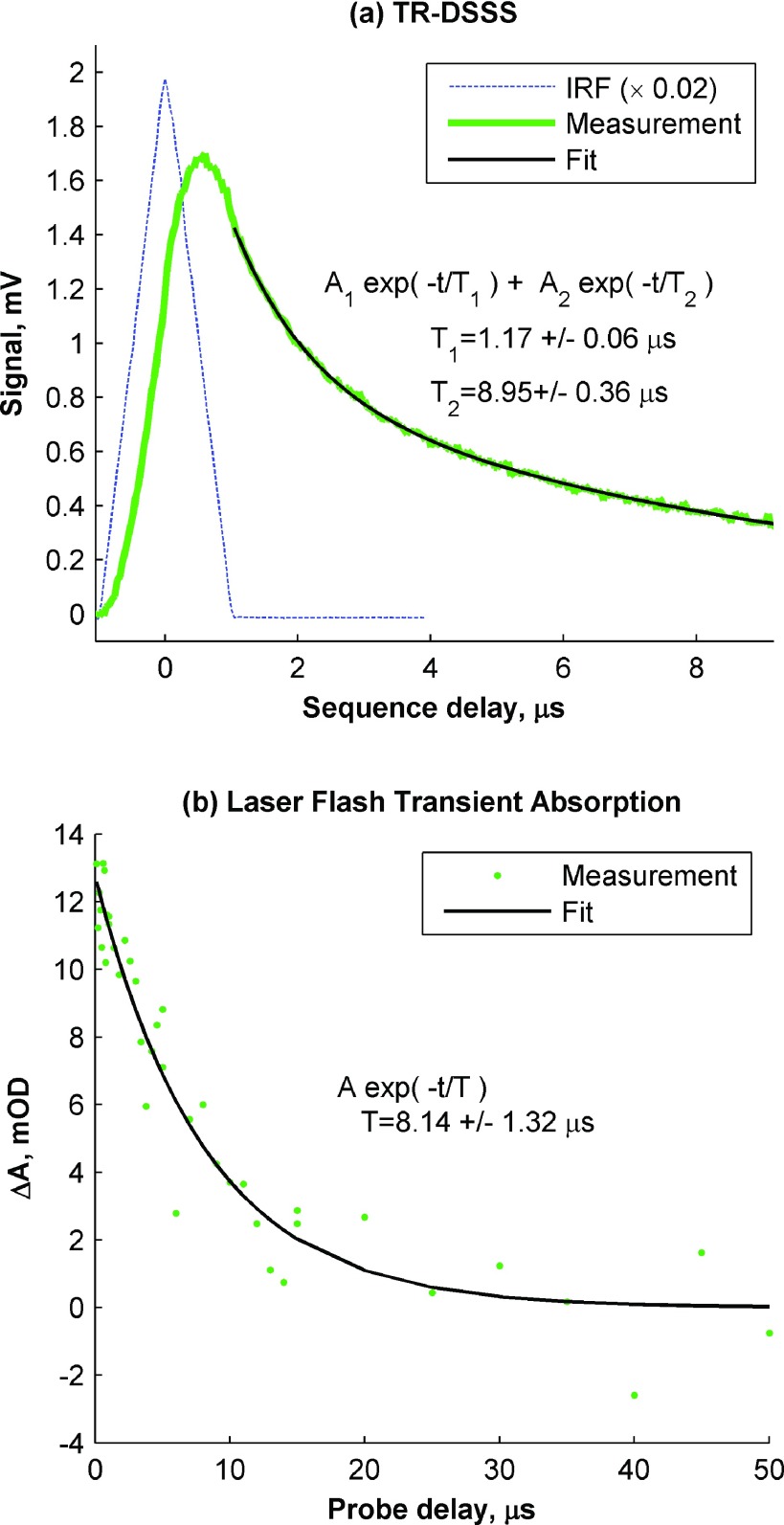
For a proof-of concept experiment, we use a porphyrin-Ru(II)polypyridyl chromophore (Pyr1RuPZnRuPyr1)29 that has a ∼9 μs triplet lifetime under oxygen-free conditions, which would normally require a laser repetition rate well below 100 kHz to ensure relaxation between subsequent pump pulses. Here, we use the same 80 MHz oscillator and optical parametric oscillator (OPO) as described before, tuned to λpu = 720 nm and λpr = 817 nm. The results are shown in Figure 6. The blue dashed line in Fig. 6(a) shows the TR-DSSS IRF, which was measured by admitting a small amount of the pump beam directly on the probe detector (100 μVpp). The IRF is the autocorrelation of the pseudo-random sequence. The 1 μs half-width reflects the 1 MS/s sequence rate (referred to as the “chip rate” in the spread-spectrum literature). The peak position at sequence delay increment 28 reflects the round-trip electronic delay of the sequence from generation to demodulation. This delay includes the FPGA auxiliary output, modulation electronics and AOM, photodetector, and FPGA digitizer input. This autocorrelation peak position is used to calibrate t = 0 delay. The TR-DSSS scan of the chromophore (with the optical delay fixed at −1 ps and scanning the electronic delay) is shown in the green line. Nonlinear fitting with MATLAB reveals a biexponential, with a long-time constant of 8.95 ± 0.36 μs (black line). For comparison, measurement with a 550 nm laser pulse excitation and a flash lamp probe in the range of 812–822 nm (the approximate bandwidth of the probe used in the TR-DSSS measurement) is shown in Figure 6(b). These data reveal a triplet state lifetime of 8.14 ± 1.32 μs. Considering the different focal conditions, excitation wavelength, and low SNR of the laser flash transient absorption measurement, the agreement between the two measurements is reasonable. These results demonstrate that a spread-spectrum approach to pump-probe can measure time-resolved dynamics, even when the relaxation timescales far exceed the laser repetition period. Here, the DSSS approach was able to resolve microsecond relaxation kinetics with an 80 MHz source (12.5 ns repetition rate). Furthermore, it is in principle possible to instantiate multiple mixers and low-pass filters on a single device, to decode multiple sequence delays simultaneously, analogous to a DSSS rake receiver30—this could enable an entire TR-DSSS delay scan to be acquired in one step.
FIG. 6.
Lifetime measurements of porphyrin-Ru(II)polypyridyl chromophore. (a) TR-DSSS measurement, along with fit to biexponential model. IRF shown for comparison. (b) Traditional laser flash transient absorption measurement, excitation 550 nm, probe 812–822 nm, along with fit to single exponential model.
IV. CONCLUSION
We have implemented a lock-in amplifier on the coprocessor FPGA of a high-speed data acquisition board and demonstrated its use in a pump-probe microscope. The FPGA approach improved imaging speed significantly, while enabling a novel approach to pump-probe detection using a spread-spectrum technique, TR-DSSS. In TR-DSSS, the pump is modulated by a pseudorandom binary sequence, so that optical transients with long relaxation timescales can be probed with high repetition rate lasers. This could provide a significant improvement for methods that detect slowly relaxing optical transients, such as photothermal microscopy28 and phosphorescence lifetime microscopy.27 In both of these, the pixel scan rate is limited by the long relaxation time—if the focal spot moves too quickly, residual signal from the previous pixels will spill over to the current pixel. A parallelized TR-DSSS approach would allow fast scanning by “tagging” the signal of each previous pixel with a unique pseudo-random code. Finally, it is our hope that this FPGA approach will enable more sophisticated real-time analysis, such as discriminating the linear and nonlinear contributions to pump-probe signals, which is becoming increasingly important in the applications of pump-probe microscopy for melanoma imaging.19,21
Acknowledgments
Research reported in this publication was supported by the National Cancer Institute of the National Institutes of Health under Award Nos. F32CA168497 (J.W.W.) and R01CA166555 (W.S.W.). The content is solely the responsibility of the authors and does not necessarily represent the official views of the National Institutes of Health. This material is based upon work supported by the National Science Foundation Division of Chemistry under Award No. 1309017 (M.C.F.).
We thank Simone Degan, Julie Kent, Christina S. Gainey, Christopher P. Dall, and Sanghamitra Deb for their assistance with the in vivo imaging experiment. We also thank Yusong Bai and J. Michael Therien for providing the porphyrin-Ru(II)polypyridyl chromophore sample and Garth Simpson and Shane Sullivan for pointers in getting started with the Alazar boards.
APPENDIX: IMPLEMENTATION DETAILS
The lock-in was implemented on an ATS-9626 data acquisition board (AlazarTech, Pointe-Claire, QC, Canada), with 250 MS/s sample rate and 16-bit analog-to-digital converter (ADC), with ±1.25 V input range, each discrete step corresponding to approximately 38 μV. Image acquisition is controlled through custom software written in C, using the LabWindows/CVI development environment (National Instruments, Austin, TX, USA). The FPGA design was implemented in VHDL (very high-speed integrated circuit hardware description language), using the Quartus II development environment (Altera, San Jose, CA, USA), targeting the Altera Stratix III EP3SL50F780C4 FPGA on the ATS-9626. Our VHDL project used the example digital downconverter project supplied by AlazarTech as a starting point. The compiled design uses 37% of the available logic elements, 30% of the embedded memory, and 45% of the DSP 18-bit multipliers.
1. Data format and representation
The ADC provides data as 16-bit unsigned values, at 250 MS/s. These are converted to 16-bit signed (two’s complement) values, representing fixed point numbers with 1 sign bit, 1 integer bit, and 14 fractional bits—Q16.14, in Qn.m format (n = total number of bits and m = number of fractional bits). Note that a 16-bit multiplication results in a 32-bit wide output, Q16.14 × Q16.14 = Q32.28. Therefore, each multiplier (except in the FIR filters) is followed by a rescaler that casts the result back to a Q16.14 number. This can introduce errors from loss of precision and saturation, which can be avoided by using floating-point numbers instead. However, floating-point operations come at the expense of reduced speed and may introduce problems with timing closure (see Subsection 4 of the Appendix).
2. Effective digitizer resolution and sample rate
Digital lock-in requires first that the input be sampled by an ADC, which, together with the analog amplifiers and filters that precede it, is the main determinant of performance characteristics such as sensitivity and input noise.2 We chose to directly sample the signal provided by the amplified photodiode rather than to use a highpass filter and/or preamplifier. This was done to avoid added noise associated with a preamplifier and to preserve the low-frequency components, which are required for DSSS de-spreading. At first glance, it may seem that this requires a digitizer with extremely high resolution to adequately sample a small probe perturbation. For example, a 1 μV modulation on a 1 V background in principle requires a million discrete levels (20 bits). However, subsequent low-pass filtering brings with it an effective bit gain.31 This allows sensitive lock-in detection with reasonably manageable ADC widths (12 bits). For example, a 16-bit ADC at 250 MS/s downsampled to 250 kS/s results in 21 effective bits output, or 1.2 μV per step. To keep this added precision, the data path after the front-end 10 × downsampler is expanded to 19 bits and the rescaler following the demodulation mixer selects a 16-bit output window that is shifted by 2 bits toward the least significant bit.
3. Output low-pass filters
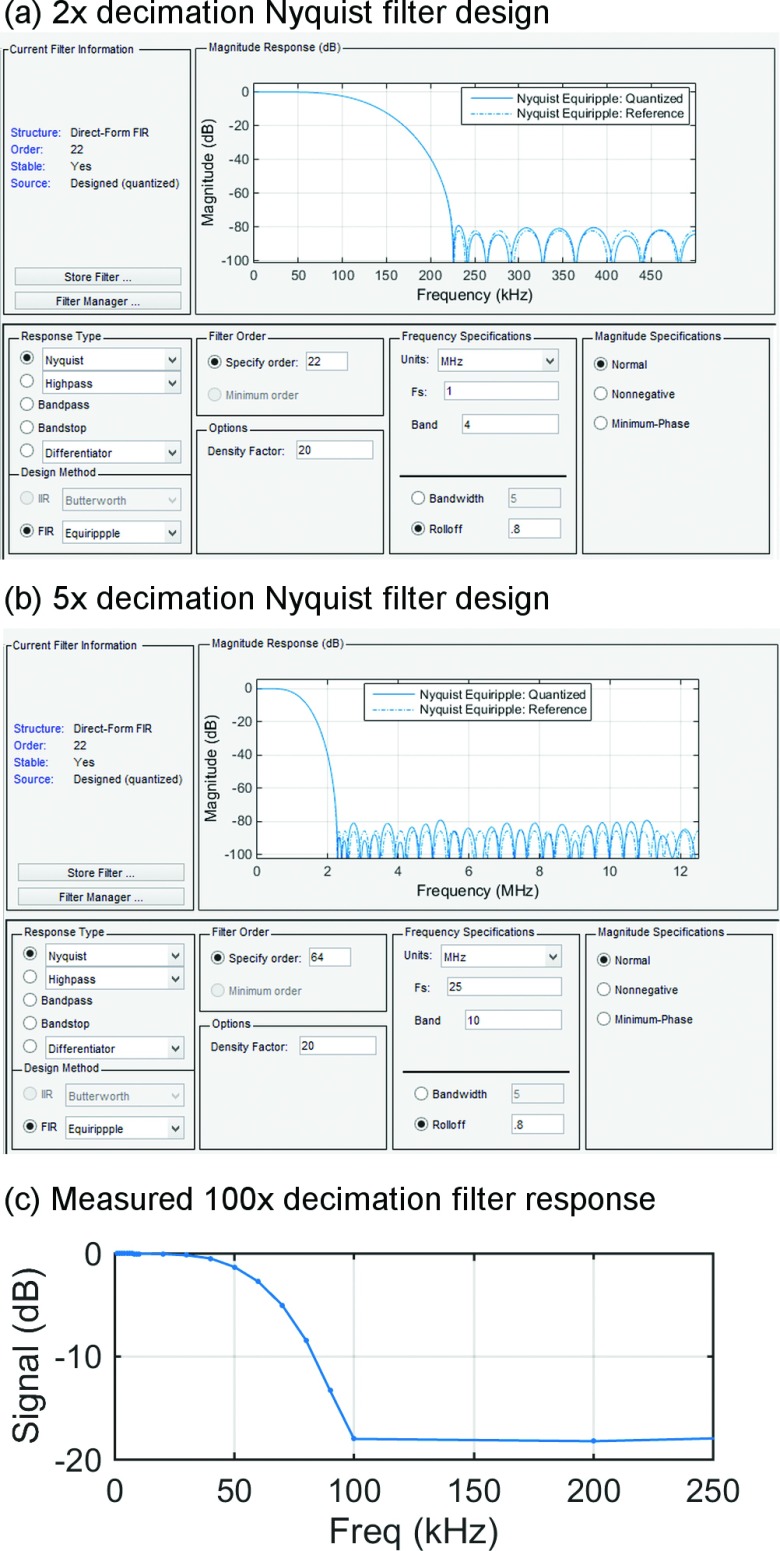
Broadly speaking, digital filters can be implemented in one of two forms: FIR and IIR. FIR filters can be more straightforward to design but may consume more resources. IIR filters use feedback, which can allow for longer-time response with fewer resources, but can be challenging to implement at high data rates, because data must finish propagating through the feedback loop before the next sample arrives. In addition, it can be challenging to design IIR filters with linear phase response (phase curvature can lead to ringing artifacts at the output). For these reasons, we implemented all filtering operations as FIR filters with linear phase. Long time constants were achieved by chaining several FIR filters together. To implement the lowpass preceding the 100 × decimation step with a single FIR filter would require 1000 filter taps; by contrast, a chain of 5 ×, 5 ×, 2 ×, and 2 × decimating filters requires only 156 taps. These filters were designed in MATLAB using the filter design and analysis tool, with the goal of minimizing frequency content above the Nyquist rate of 125 kHz, for the 250 kS/s output. The position of the 16-bit output slice was selected to maintain approximately unity gain through the filter. Design parameters for the individual filters and response of the composite 100 × decimating low-pass filters are shown in Figure 7.
FIG. 7.
100 × decimating lowpass filter design and validation. MATLAB fdatool parameters and theoretical response for the 2 × stage shown in (a) and the 5 × stage shown in (b). Measured response of the composite 100 × decimation filter shown in (c).
4. Timing and synchronization
Here, we discuss several aspects of timing and synchronization related to the DSP lock-in: pixel clock synchronization with a secondary data acquisition board, timing closure within the design, and reference wave synchronization with the pump modulation. Pixel clocks are synchronized by driving the ATS-9626 master 250 MHz ADC clock with a phase-locked loop (PLL) that is locked to a 10 MHz reference supplied by the NI-DAQ board.
Timing closure is very important for high-speed FPGA circuits. A mismatch in propagation delay between different data paths that exceeds one clock period can lead to serious problems. Because our target demodulation frequency is only 1–10 MHz, we can relax these timing constraints by first downsampling the incoming 250 MS/s data stream to 25 MS/s and perform all DSP operations at 25 MHz, a factor of 10 below the maximum clock rate of the ATS-9626. The 25 MHz DSP clock is derived from the master 250 MHz clock by a PLL. In addition, we perform all arithmetic in signed fixed-point format rather than floating point, for the sake of increased speed (a 16-bit floating point multiply requires 4 × 250 MHz clock cycles, while a 16-bit fixed-point multiply requires only one).
As described in the text earlier, the reference waveform is derived from an external transistor-transistor logic (TTL) signal as follows. The TTL is cast as a square wave and filtered through a narrow-band 2 MHz IIR filter to produce a sinusoidal waveform. A quadrature reference is produced by numerically differentiating the reference wave and an arbitrarily phase-shifted reference is produced by summing the in-phase and quadrature references in varying proportion.
REFERENCES
- 1.King J. D., Makowski M. A., Holcomb C. T., Allen S. L., Geer R., Meyer W. H., Hill D. N., Pham D., and Morse E. C., Rev. Sci. Instrum. 81(10), 10D739 (2010). 10.1063/1.3496989 [DOI] [PubMed] [Google Scholar]
- 2.Lascos S. J. and Cassidy D. T., Rev. Sci. Instrum. 79(7), 074702 (2008). 10.1063/1.2956974 [DOI] [PubMed] [Google Scholar]
- 3.Restelli A., Abbiati R., and Geraci A., Rev. Sci. Instrum. 76(9), 093112 (2005). 10.1063/1.2008991 [DOI] [Google Scholar]
- 4.Shirvaikar M. and Bushnaq T., Proc. SPIE 7244, 724406 (2009). 10.1117/12.806099 [DOI] [Google Scholar]
- 5.Pickholtz R. L., Schilling D. L., and Milstein L. B., IEEE Trans. Commun. 32(2), 211-212 (1984). 10.1109/TCOM.1984.1096025 [DOI] [Google Scholar]
- 6.McGraw C. M., Khalil G., and Callis J. B., J. Phys. Chem. C 112(21), 8079-8084 (2008). 10.1021/jp711867u [DOI] [Google Scholar]
- 7.Min W., Freudiger C. W., Lu S. J., and Xie X. S., Annu. Rev. Phys. Chem. 62, 507-530 (2011). 10.1146/annurev.physchem.012809.103512 [DOI] [PMC free article] [PubMed] [Google Scholar]
- 8.Zipfel W. R., Williams R. M., and Webb W. W., Nat. Biotechnol. 21(11), 1368-1376 (2003). 10.1038/nbt899 [DOI] [PubMed] [Google Scholar]
- 9.Vogel A., Noack J., Huttman G., and Paltauf G., Appl. Phys. B 81(8), 1015-1047 (2005). 10.1007/s00340-005-2036-6 [DOI] [Google Scholar]
- 10.Clarke G. M., Eidt S., Sun L., Mawdsley G., Zubovits J. T., and Yaffe M. J., Histopathology 50(2), 232-242 (2007). 10.1111/j.1365-2559.2006.02561.x [DOI] [PubMed] [Google Scholar]
- 11.Robles F. E., Fischer M. C., and Warren W. S., Opt. Lett. 39(16), 4788-4791 (2014). 10.1364/OL.39.004788 [DOI] [PMC free article] [PubMed] [Google Scholar]
- 12.Wahlstrand J. K., Merlin R., Li X. Q., Cundiff S. T., and Martinez O. E., Opt. Lett. 30(8), 926-928 (2005). 10.1364/OL.30.000926 [DOI] [PubMed] [Google Scholar]
- 13.Wilson J. W., Schlup P., and Bartels R. A., Chem. Phys. Lett. 463(4-6), 300-304 (2008). 10.1016/j.cplett.2008.08.067 [DOI] [Google Scholar]
- 14.Saar B. G., Freudiger C. W., Reichman J., Stanley C. M., Holtom G. R., and Xie X. S., Science 330(6009), 1368-1370 (2010). 10.1126/science.1197236 [DOI] [PMC free article] [PubMed] [Google Scholar]
- 15.Slipchenko M. N., Oglesbee R. A., Zhang D. L., Wu W., and Cheng J. X., J. Biophotonics 5(10), 801-807 (2012). 10.1002/jbio.201200005 [DOI] [PubMed] [Google Scholar]
- 16.Seto K., Tsukada T., Okuda Y., Tokunaga E., and Kobayashi T., Rev. Sci. Instrum. 85(2), 023702 (2014). 10.1063/1.4863879 [DOI] [PubMed] [Google Scholar]
- 17.Dewalt E. L., Sullivan S. Z., Schmitt P. D., Muir R. D., and Simpson G. J., Anal. Chem. 86(16), 8448-8456 (2014). 10.1021/ac502124v [DOI] [PMC free article] [PubMed] [Google Scholar]
- 18.Matthews T. E., Wilson J. W., Degan S., Simpson M. J., Jin J. Y., Zhang J. Y., and Warren W. S., Biomed. Opt. Express 2(6), 1576-1583 (2011). 10.1364/BOE.2.001576 [DOI] [PMC free article] [PubMed] [Google Scholar]
- 19.Wilson J. W., Degan S., Gainey C. S., Mitropoulos T., Simpson M. J., Zhang J. Y., and Warren W. S., J. Biomed. Opt. 20(5), 051012 (2015). 10.1117/1.JBO.20.5.051012 [DOI] [PMC free article] [PubMed] [Google Scholar]
- 20.Wilson J. W., Degan S., Mitropoulos T., Selim M. A., Zhang J. Y., and Warren W. S., Proc. SPIE 8226, 822602 (2012). 10.1117/12.908821 [DOI] [Google Scholar]
- 21.Simpson M. J., Wilson J. W., Robles F. E., Dall C. P., Glass K., Simon J. D., and Warren W. S., J. Phys. Chem. A 118(6), 993-1003 (2014). 10.1021/jp4107475 [DOI] [PMC free article] [PubMed] [Google Scholar]
- 22.Redford G. I. and Clegg R. M., J. Fluoresc. 15(5), 805-815 (2005). 10.1007/s10895-005-2990-8 [DOI] [PubMed] [Google Scholar]
- 23.Lakowicz J. R., Cherek H., Gryczynski I., Joshi N., and Johnson M. L., Biophys. Chem. 28(1), 35-50 (1987). 10.1016/0301-4622(87)80073-X [DOI] [PMC free article] [PubMed] [Google Scholar]
- 24.Collier B. B. and McShane M. J., J. Lumin. 144, 180-190 (2013). 10.1016/j.jlumin.2013.06.034 [DOI] [Google Scholar]
- 25.Kohno R., Meidan R., and Milstein L. B., IEEE Commun. Mag. 33(1), 58-67 (1995). 10.1109/35.339882 [DOI] [Google Scholar]
- 26.Viterbi A. J., CDMA: Principles of Spread Spectrum Communication (Addison-Wesley Pub. Co., Reading, Massachusetts, 1995). [Google Scholar]
- 27.Finikova O. S., Lebedev A. Y., Aprelev A., Troxler T., Gao F., Garnacho C., Muro S., Hochstrasser R. M., and Vinogradov S. A., ChemPhysChem 9(12), 1673-1679 (2008). 10.1002/cphc.200800296 [DOI] [PMC free article] [PubMed] [Google Scholar]
- 28.Nedosekin D. A., Galanzha E. I., Ayyadevara S., Reis R. J. S., and Zharov V. P., Biophys. J. 102(3), 672-681 (2012). 10.1016/j.bpj.2011.12.035 [DOI] [PMC free article] [PubMed] [Google Scholar]
- 29.Olivier J.-H., Bai Y., Uh H., Yoo H., Therien M. J., and Castellano F. N., “Near infrared-to-visible photon upconversion enabled by highly conjugated sensitizers under low-power noncoherent illumination” (unpublished). [DOI] [PubMed]
- 30.Cheun K. W., IEEE Trans. Commun. 45(9), 1130-1143 (1997). 10.1109/26.623079 [DOI] [Google Scholar]
- 31.Baker B., EDN 50(4), 26 (2005). [Google Scholar]


