

Abstract
For several years, graphene has been the focus of much attention due to its peculiar characteristics, and it is now considered to be a representative 2-dimensional (2D) material. Even though many research groups have studied on the graphene, its intrinsic nature of a zero band-gap, limits its use in practical applications, particularly in logic circuits. Recently, transition metal dichalcogenides (TMDs), which are another type of 2D material, have drawn attention due to the advantage of having a sizable band-gap and a high mobility. Here, we report on the design of a complementary inverter, one of the most basic logic elements, which is based on a MoS2 n-type transistor and a WSe2 p-type transistor. The advantages provided by the complementary metal-oxide-semiconductor (CMOS) configuration and the high-performance TMD channels allow us to fabricate a TMD complementary inverter that has a high-gain of 13.7. This work demonstrates the operation of the MoS2 n-FET and WSe2 p-FET on the same substrate, and the electrical performance of the CMOS inverter, which is based on a different driving current, is also measured.
Keywords: Transition metal dichalcogenide (TMD), CMOS inverter, 2-Dimensional material
Background
With the advent of graphene, one of the most studied 2-dimensional (2D) materials, layered materials attracted much attention due to their unique and outstanding electrical, mechanical, and optical characteristics [1,2]. In spite of having an extremely high mobility of 15,000 cm2/Vs and of being easy to scale down, the absence of an inherent band-gap limits the potential for graphene to be implemented in logic circuits [3].
Transition metal dichalcogenides (TMDs) are a family of 2D materials and are considered to be good candidate materials that can overcome the limitations of graphene. TMDs follow the formula MX2, where M is a transition metal and X stands for a chalcogen (S, Se, Te, etc.). TMD consists of atomic layers that have very weak van der Waals forces binding them, and they usually have a band-gap of 1.1 to 1.9 eV [4]. Such properties enable TMDs to be used as channel materials in high-performance field-effect transistors (FET) [5]. Of the various TMD materials available, MoS2 and WSe2 have been individually reported to be suitable channel materials for n-type and p-type transistors. The MoS2 n-FET demonstrated a mobility of approximately 200 cm2/Vs, and an effective hole mobility for WSe2 p-FET of up to approximately 250 cm2/Vs was also reported [6,7].
A complementary metal-oxide-semiconductor (CMOS) inverter is a fundamental unit for the logic elements of a circuit. In order to fabricate a CMOS inverter, both p-type and n-type transistors are necessary [8]. In comparison to a resistive-load inverter, a complementary inverter presents outstanding properties in terms of having low power consumption and a large noise margin [9].
There have been several studies trying to fabricate complementary inverter using TMDs. Huang J et al. [9] have reported the first CMOS inverter using TMD, which was fabricated with MoS2 and carbon nanotube as channel materials. After this report, researchers tried several other p-channel materials like Bi2Sr2Co2O8 [10] or phosphorene [11], and fabricated complementary inverter with a combination of MoS2. Such reports possess significance in that both n-channel and p-channel are layered materials, but still, the electrical performances of the devices were insufficient. The first fully TMD-based CMOS inverter was achieved by Tosun M et al. [12] by utilizing one material of WSe2. For p-channel, pure WSe2 was used and for n-channel, K-doped WSe2 was used. The resulting device exhibited high peak gain of approximately 12, but due to the instability of K doping in air, its performance tends to degrade as operation time goes on. Recently, Das S et al. [13] have reported WSe2-based complementary inverter showing a gain of over 25. As they carefully engineered the threshold voltage of both n-FET and p-FET which constitutes the CMOS inverter, the resulting device property was remarkable.
Here, we report on a fully TMD-based CMOS inverter which is comprised of a MoS2 n-FET and a WSe2 p-FET. The peak gain for our complementary TMD inverter reaches a value of over 13 at a driving voltage of 2 V. We used two different intrinsic n-type and p-type TMDs individually, and achieved a reasonable performance of MoS2-/WSe2-based CMOS inverter which could be a great potential of TMDs in logic applications.
Methods
Several layers of each TMD were obtained from commercially available bulk MoS2 (429ML-AB, SPI Supplies Inc., West Chester, PA, USA) and WSe2 (NS00182, Nanoscience Instruments Inc., Phoenix, AZ, USA) crystals via mechanical exfoliation using an adhesive tape. A highly-doped silicon substrate with a 30-nm-thick atomic layer deposition (ALD) Al2O3 was used to fabricate the complementary TMD inverter. Multi-layer MoS2 was transferred onto half the area of one substrate, and WSe2 was transferred onto the other half. Then, 200 μm × 200 μm square electrode arrays were fabricated for each channel material through a conventional lift-off process. In order to form ohmic contacts, the 30 nm Ti and 30 nm Pt were individually used as the metals for the electrical contacts of the n-FET and p-FET by considering the work functions of MoS2 and WSe2. After fabricating the n-FETs and p-FETs on one substrate, a Keithley 4200 parameter analyzer was used to measure the electrical performance of the MoS2 and WSe2 FETs.
Based on the results of the measurements, we chose several sets of n-FETs and p-FETs that showed a reasonable performance. Finally, a 50-nm-thick Ti connecting line was fabricated between the selected MoS2 and WSe2 FETs through a lift-off process, and it was followed by electron-beam deposition. After the CMOS inverter structure was fabricated, the devices underwent annealing for 2 h in a tube furnace at 200°C with an N2 atmosphere in order to decrease the contact resistance between the channel and the metal electrode. A Keithley 4200 parameter analyzer was used to measure the electrical performance of the MoS2/WSe2 CMOS inverter. The measurements were carried out using four probes to plot the graph for the input and output voltage of the inverter. The driving voltage (VDD) was applied to the source of the p-FET, and ground was connected to the source of the n-FET. The input voltage was applied to the bottom gate of MoS2 FET and WSe2 FET at the same time by sweeping from −5 to 0 V, and the output voltage was recorded by measuring at the connecting line for both drains.
Results and discussion
Figure 1 depicts the overall structure of the TMD CMOS inverter that contains both an n-FET and a p-FET with TMDs as channel materials. We used multi-layer MoS2 for the n-type channel and multi-layer WSe2 for the p-type semiconducting material (Figure 2a,b). Ti was chosen as the metal electrode for the MoS2 FET since that metal is known to have a small work function, and it is therefore easier to form an ohmic contact with MoS2 [4]. On the other hand, WSe2 has unique characteristic in that a simultaneous injection of both holes and electrons can easily occur, resulting in ambipolar transport [5,7]. In order to meet our goals for fabricating the p-type FET, a metal with a large work function had better be used for the electrode. Therefore, we chose Pt for the WSe2 FET since Pt has a work function of 5.12 to 5.93 eV.
Figure 1.
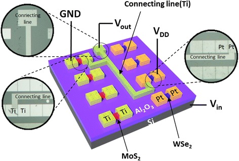
Device structure with electrical connections. Schematic illustration and optical microscopy image of a MoS2/WSe2 complementary inverter with electrical connections that were used to measure the electrical characteristics.
Figure 2.
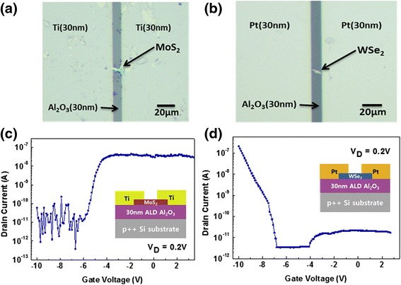
Optic images and transfer characteristics of n- FET and p- FET. Optical microscopic image of (a) the MoS2 n-FET and (b) the WSe2 p-FET that was employed to fabricate the TMD CMOS inverter. The transfer characteristics of (c) the MoS2 n-FET and (d) the WSe2 p-FET at a drain voltage of 0.2 V.
The transfer characteristics were measured in order to verify the electrical performance of the FETs. Figure 2c,d presents the resulting transfer curves for the n-FET and p-FET. The MoS2 FET shown in Figure 2c has 6-μm channel width and 10-μm channel length. It shows clear n-type characteristics with an Ion/Ioff ratio of approximately 105. As the gate voltage increases to be higher than the threshold voltage (−5.23 V), the drain current drastically increases up to approximately 10−7 A. The field-effect mobility of the MoS2 FET derived from the transfer characteristic is found to be 0.86. The WSe2 FET presents p-type characteristics caused by the hole injection. The drain current tends to increase sharply, up to approximately 10−7 A, under a gate bias that is less than its threshold voltage, −8.79 V. This device with 2-μm channel width and 10-μm channel length exhibits Ion/Ioff ratio of approximately 104 and mobility of 8.87. Both the n-FET and p-FET show a moderate current on-off ratio with a similar on-current level, which is one of the key requirements to work as a complementary inverter.
After sorting MoS2 n-FET and WSe2 p-FET presenting reasonable electrical performances, CMOS inverter was fabricated with them. The two FETs were connected in series, n-FET drain-by-p-FET drain, with a metal line in order to have them work together as a logic inverter. As shown in Figure 1, the electrical connection was configured to measure the performance of the completed complementary TMD inverter. Four probes were used to apply the voltage and to record the output voltage. A constant bias of VDD = 2 V was applied, and the relation between the input voltage and the output voltage was measured as shown in Figure 3. The voltage transfer characteristic in Figure 3 was measured from the TMD CMOS inverter consists of n-FET and p-FET indicated at Figure 2c,d, respectively. While the device received a low-input voltage, the p-type WSe2 FET was left in the ‘on’ state and the n-type MoS2 FET was in the ‘off’ state. Hence, the output voltage remained high, near VDD. On the other hand, the n-type MoS2 FET was in the on state, and the p-type WSe2 FET was in the off state when a high input was applied. As a result, an output voltage of 0 V was measured, which indicates that logic operation from 1 to 0 was performed. Such a voltage transfer curve clearly demonstrates the characteristics of an inverter.
Figure 3.
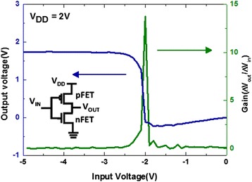
Voltage transfer characteristics of the inverter. Voltage transfer characteristics and gain curve of a MoS2/WSe2 complementary inverter at a V DD of 2V.
From the input–output voltage plot, the gain curve can be calculated as ΔVout/ΔVin. As shown in Figure 3, the peak in the gain curve shows the transition point for the inverter. In our work, the peak gain of the MoS2/WSe2 complementary inverter reaches 13.7, which is a considerably high value when compared to CMOS inverters based on other 2D material FETs. Table 1 presents a summary of the complementary inverters that have been reported along with their peak gain. Several reports have discussed the fabrication of a CMOS inverter and a pseudo-CMOS inverter (an inverter configuration using two ambipolar transistors rather than one n-FET and one p-FET) based on 2D materials. However, a fully TMD-based inverter has only been discussed by Tosun et al. [12] and S Das et al. [13] who used n-type- and p-type-doped WSe2 as the channel materials. It is thought that the characteristics of the inverter proposed in this work are remarkable since it has been fabricated by using TMDs for both the n-channel and the p-channel, with different channel materials. In addition, a peak gain of over 13 is a relatively high value when compared to not only 2D material-based CMOS inverters but also to those based on oxides or organic materials as well (Table 1). It is considered that the fabrication of such a high-performance inverter in our work was accomplished due to the integration of high-mobility TMD materials and a CMOS configuration.
Table 1.
Summary of the CMOS inverter peak gain based on various channels
| Channel material | ||||
|---|---|---|---|---|
| Inverter peak gain | Ref. | |||
| n-type | p-type | |||
| 2D material | MoTe2 (ambipolar) | 1.4 | [14] | |
| WSe2 | WSe2 | 12 | [12] | |
| WSe2 | WSe2 | 25 | [13] | |
| MoS2 | Carbon nanotube | 1.3 | [9] | |
| MoS2 | Phosphorene | 1.4 | [11] | |
| MoS2 | BSCO | 1.7 | [10] | |
| MoS2 | WSe2 | 13.7 | This work | |
| Silcon | Si-nanowire | Si-nanowire | 45 | [15] |
| Oxide | GIZO | SnO | 1.7 | [16] |
| Organic | OC1C10-PPV:PCBM blend (ambipolar) | 10 | [17] | |
In order to further investigate the electrical performance, we changed the driving voltage over three steps, 1, 2, and 3 V, and performed measurements the according voltage transfer characteristics. Figure 4a shows the electrical characteristics of the various voltages used to drive the circuit voltage, and Figure 4b presents the gain plot extracted from the transfer curve. As shown in Figure 4a, our device operates under a negative input voltage. The switching threshold voltage (VM) of the inverter, which represents the voltage at which the n-FET and p-FET are turned on with the same intensity, is also located in the negative region. These phenomena are all associated with the threshold voltage of the n-FET and the p-FET. Usually the threshold voltage of an n-type transistor has a positive value and that of a p-type transistor has negative value, so the switching threshold voltage is generally located in the range from 0 V to VDD. However, in our work, both the MoS2 FET and the WSe2 FET have negative threshold voltages. Accordingly, the equations
| 1 |
Figure 4.
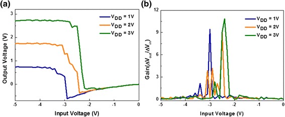
Electrical properties of the TMD inverter. (a) Voltage transfer characteristics and (b) gain curve for a MoS2/WSe2 complementary inverter at different driving voltages (V DD).
can be applied where VTn and VTp are the threshold voltage of the n-FET and p-FET respectively, W is width of the channel, L is the length of channel, μ is the mobility of the FET, and Cox is the capacitance of the oxide per unit area. As such, the switching threshold voltage is calculated to be −7.10, −6.37, and −5.64 Vwhen VDD = 1, 2, and 3 V, respectively. The positive shift in the voltage transfer curve is due to the shift in the switching threshold voltage, which is also demonstrated in Figure 4a.
As the driving voltage for the inverter changes, the peak gain also changes (Figure 4b). The device tended to show higher gain value as the driving voltage increases. Also, the peak gain appeared at higher input voltage along with the increase of VDD from 1 to 3 V. Such phenomena coincide with the well-known operating characteristics of a CMOS inverter.
The electrical property of the TMD CMOS inverter shown in Figure 4 is inferior to the one shown in Figure 3. Such degradation is mainly caused by the environmental effects which are often observed in TMD transistors [18]. As the electrical characteristic under various driving voltage was measured after several days of device fabrication, moisture around the environment might be absorbed to the surface of channel. Uniform encapsulation of the inverter structure will minimize the environmental effects and remain its property under ambient condition.
Conclusions
In summary, we have fabricated a CMOS inverter by employing an n-type MoS2 FET and a p-type WSe2 FET to achieve a gain of 13.7. The device clearly operates as a logic inverter by changing the low-input voltage into a high-output voltage and vice versa. The working range observed in the negative region is caused by the negative threshold voltage of the n-FET. It is considered that this result is meaningful in that the complementary inverter used two different kinds of TMD materials for the channels, and it exhibits relatively high performance compared to those of devices based on other 2D materials which had been previously reported. This result will provide a step forward towards the fabrication of logic circuits applying TMD materials as a post-Si generation device.
Acknowledgements
This research was supported by the MSIP (Ministry of Science, ICT, and Future Planning), Korea, under the “IT Consilience Creative Program” (NIPA-2014-H0201-14-1002) supervised by the NIPA (National IT Industry Promotion Agency).
Footnotes
Competing interests
The authors declare that they have no competing interests.
Authors' contributions
A-JC carried out the experiments on fabrication of TMD CMOS inverter and electrical measurement of the device. A-CC also drafted the manuscript. KCP contributed the analysis on resulting electrical characteristics of our device. J-YK supervised the work and reviewed the manuscript. All authors read and approved the final manuscript.
Contributor Information
Ah-Jin Cho, Email: ahjincho@yonsei.ac.kr.
Kee Chan Park, Email: keechan@konkuk.ac.kr.
Jang-Yeon Kwon, Email: jangyeon@yonsei.ac.kr.
References
- 1.Castro Neto AH, Guinea F, Peres NMR, Novoselov KS, Geim AK. The electronic properties of graphene. Rev Mod Phys. 2009;81:109–62. doi: 10.1103/RevModPhys.81.109. [DOI] [Google Scholar]
- 2.Hsu P-L. Choosing a gate dielectric for graphene based transistors. Master thesis. Cambridge: Massachusetts Institute of Technology, Electrical Engineering and Computer Science Department; 2008. [Google Scholar]
- 3.Geim AK, Novoselov KS. The rise of graphene. Nat Mater. 2007;6:183–91. doi: 10.1038/nmat1849. [DOI] [PubMed] [Google Scholar]
- 4.Wang ZM. MoS2 materials, physics, and devices. New York: Springer; 2014. [Google Scholar]
- 5.Radisavljevic B, Whitwick MB, Kis A. Integrated circuits and logic operations based on single-layer MoS2. ACS NANO. 2011;5:9934–8. doi: 10.1021/nn203715c. [DOI] [PubMed] [Google Scholar]
- 6.Radisavljevic B, Radenovic A, Brivio J, Giacometti V, Kis A. Single-layer MoS2 transistors. Nat Nanotechnol. 2011;6:147–50. doi: 10.1038/nnano.2010.279. [DOI] [PubMed] [Google Scholar]
- 7.Fang H, Chuang S, Chang TC, Takei K, Takahashi T, Javey A. High-performance single layered WSe2 p-FETs with chemically doped contacts. Nano Lett. 2012;12:3788–92. doi: 10.1021/nl301702r. [DOI] [PubMed] [Google Scholar]
- 8.Baker RJ. CMOS circuit design, layout, and simulation. London: Wiley-Interscience; 2005. [Google Scholar]
- 9.Huang J, Somu S, Busnaina A. A molybdenum disulfide/carbon nanotube heterogeneous complementary inverter. Nanotechnology. 2012;23:1–5. doi: 10.1155/2012/214783. [DOI] [PubMed] [Google Scholar]
- 10.Yu WJ, Li Z, Zhou H, Chen Y, Wang Y, Huang Y, et al. Vertically stacked multi-heterostructures of layered materials for logic transistors and complementary inverters. Nat Mat. 2013;12:246–52. doi: 10.1038/nmat3518. [DOI] [PMC free article] [PubMed] [Google Scholar]
- 11.Liu H, Neal AT, Zhu Z, Luo Z, Xu X, Tomanek D, et al. Phosphorene: an unexplored 2D semiconductor with a high hole mobility. ACS Nano. 2014;8:4033–41. doi: 10.1021/nn501226z. [DOI] [PubMed] [Google Scholar]
- 12.Tosun M, Chuang S, Fang H, Sachid AB, Hettick M, Lin Y, et al. High-gain inverters based on WSe2 complementary field-effect transistors. ACS Nano. 2014;8:4948–53. doi: 10.1021/nn5009929. [DOI] [PubMed] [Google Scholar]
- 13.Das S, Dubey M, Roelofs A. High gain, low noise, fully complementary logic inverter based on bi-layer WSe2 field effect transistors. Appl Phys Lett. 2014;105:083511. doi: 10.1063/1.4894426. [DOI] [Google Scholar]
- 14.Lin Y-F, Xu Y, Wang S-T, Li S-L, Yamamoto M, Aparecido-Ferreira A, et al. Ambipolar MoTe2 transistors and their applications in logic circuits. Adv Mat. 2014;26:3263–9. doi: 10.1002/adma.201305845. [DOI] [PubMed] [Google Scholar]
- 15.Buddharaju KD, Singh N, Fustagi SC, Teo SHG, Lo GQ, Balasubramanian N, et al. Si-nanowire CMOS inverter logic fabricated using gate-all-around devices and top-down approach. Solid State Electron. 2008;52:1312–7. doi: 10.1016/j.sse.2008.04.017. [DOI] [Google Scholar]
- 16.Barquinha P, Martins R, Pereira L, Fortunato E. Transparent oxide electronics: from materials to devices. London: Wiley; 2012. [Google Scholar]
- 17.Meijer EJ, De Leeuw DM, Setayesh S, Van Veenendaal E, Huisman B-H, Blom PWM, et al. Solution-processed ambipolar organic field-effect transistors and inverters. Nat Mat. 2003;2:678–82. doi: 10.1038/nmat978. [DOI] [PubMed] [Google Scholar]
- 18.Late DJ, Liu B, Ramakrishna Matte HSS, Dravid VP, Rao CNR. Hysteresis in single-layer MoS2 field effect transistors. ACS NANO. 2012;6:5635–41. doi: 10.1021/nn301572c. [DOI] [PubMed] [Google Scholar]