Abstract
As defects frequently govern the properties of crystalline solids, the precise microscopic knowledge of defect atomic structure is of fundamental importance. We report a new class of point defects in single-layer transition metal dichalcogenides that can be created through 60° rotations of metal–chalcogen bonds in the trigonal prismatic lattice, with the simplest among them being a three-fold symmetric trefoil-like defect. The defects, which are inherently related to the crystal symmetry of transition metal dichalcogenides, can expand through sequential bond rotations, as evident from in situ scanning transmission electron microscopy experiments, and eventually form larger linear defects consisting of aligned 8–5–5–8 membered rings. First-principles calculations provide insights into the evolution of rotational defects and show that they give rise to p-type doping and local magnetic moments, but weakly affect mechanical characteristics of transition metal dichalcogenides. Thus, controllable introduction of rotational defects can be used to engineer the properties of these materials.
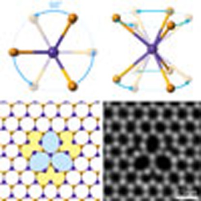 Defects in a crystalline solid can have a dramatic effect on the material’s properties. Here, the authors demonstrate a class of defects in two-dimensional transition metal dichalcogenides mediated by chalcogen vacancies and inherently related to the crystal symmetry
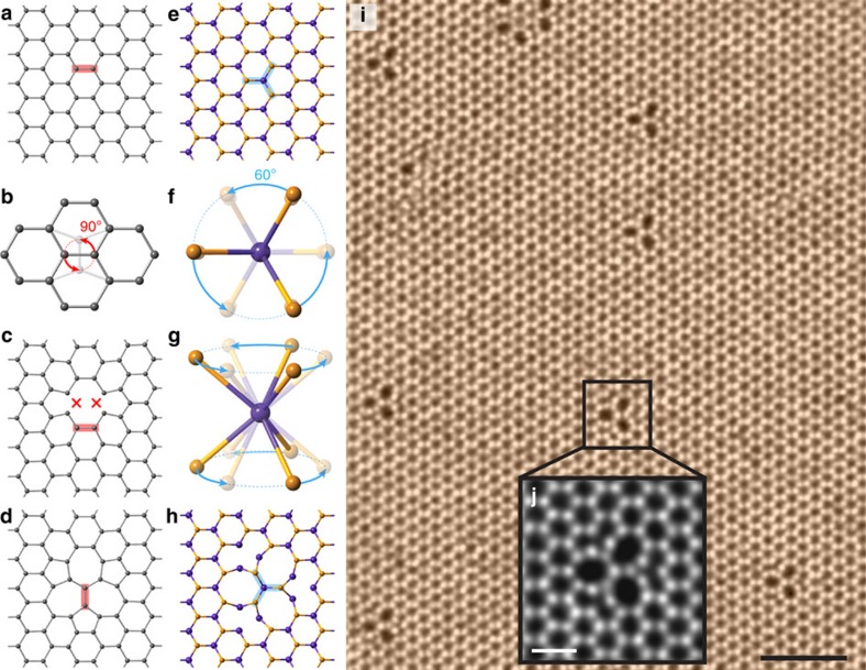
Point and line defects strongly influence electronic, optical, thermal and mechanical properties of solids, either with overall detrimental (for example, defect-induced embrittlement of reactor steels) or beneficial (doping of semiconductors) effect on the materials characteristics, calling on careful investigations of their atomic structure. Aberration-corrected transmission electron microscopy (TEM) made it possible to study the structure and behaviour of defects on atomic scale in real time, and has provided many insights into defect dynamics. In sp2-hybridized hexagonal carbon systems, for example, carbon nanotubes1 or graphene2,3, Stone–Wales transformations4 representing rotations of C–C bonds by 90° (Fig. 1a,b) have been observed. Such transformations can be regarded as an elementary step that not only gives rise to topological defects5,6, but are also responsible for plastic deformation7,8, rippling9 and grain boundary motion10.
Figure 1. Model of rotational defect in graphene and TMDs.
(a) Atomic model of graphene. (b) Top view of the Stone–Wales transformation, showing 90° rotation of a carbon bond. (c) Atomic model of graphene with a divacancy. (d) The atomic model of SW-transformed graphene divacancy. (e) Atomic model of TMDs with a structural formula MX2, the top view. The orange spheres represent chalcogen atoms, the blue ones the metal atoms. (f,g) Triple M–X bonds showing 60° rotation from the top and perspective views. (h) The atomic model of trefoil defect. Three M–X bond pairs marked by blue bars are 60° rotated from those in e. (i) A typical ADF image of WSe2 observed at 500 °C. The density of trefoil defect is found to be about 5.1%. Scale bar, 2 nm. (j) The magnified ADF image from the black square in i. Scale bar, 0.5 nm.
In two-dimensional (2D) materials with trigonal symmetry, for example, h-BN11,12,13,14 or transition metal dichalcogenides (TMDs)15,16,17,18,19,20, point and line defects have been observed, but Stone–Wales rotational defects are not expected due to the polar nature of chemical bonds in such systems. On the other hand, a 60° rotation of three bonds centred on a metal atom, as schematically shown in Fig. 1e–g, would preserve the heteroatomic nature of bonding and the trigonal lattice symmetry, resulting in the formation a ‘trefoil’-shaped defect (Fig. 1h). This gives rise to the fundamental question: can such transformations occur in stoichiometric or atom-deficient 2D systems with trigonal symmetry, and if yes, what kind of defects they would produce and how would these defects affect the properties of the material.
In the following, we present observations of such rotational defects. By combing scanning TEM (STEM) experiments with first-principles calculations, we show that such rotational defects exist in chalcogen-deficient TMDs and that the trefoil defect (Fig. 1j) is the simplest example in a series of bond rotation-mediated transformations in the TMDs. By sequential rotations of metal–chalcogen (M–X) bonds, the rotational defects can expand in size and also migrate in the lattice, or form one-dimensional domain boundaries. The formation and evolution of the defects are mediated by chalcogen vacancies induced by the electron-beam irradiation.
Results
Atomic structure of rotational defects in TMDs
Figure 1i presents examples of trefoil defects in WSe2, which were found abundant at elevated temperatures. A comparison of the experimental STEM images with the simulated ones based on possible atomic structures (Supplementary Fig. 2) indicated that the system is Se deficient due to electron-beam irradiation. Similar trefoil-shaped defects also exist in graphene as reconstructed divacancies, but there the C–C bond is rotated by 90° as shown in Fig. 1c,d.
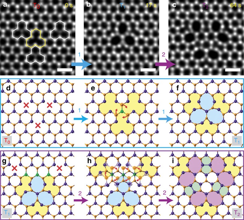
Figure 2a–c shows the filtered annular dark-field (ADF) images of three different Se-deficient WSe2 structures. In Fig. 2a, one can see two distinct image contrasts of the vacancies at the Se sites, corresponding to single Se vacancies (SVSe, white polygon) and double vacancies (DVSe, yellow polygon), respectively. At t=17 s, a new WSe2 defect of three-fold rotational symmetry, consisting of three eight-membered rings, resembling a trifoliate leaf, suddenly appears (Fig. 2b). We designate this three-fold symmetrical trefoil defect as the ‘first-order rotational defect’ or ‘T1’ (with the lattice keeping the original symmetry being ‘T0’). A model of the defect transformation from T0 to T1 is presented in Fig. 2d–f. The trefoil defects were always observed in W-centred configuration, but never in the equally possible Se-centred configuration, indicating the crucial role of the Se vacancies in the formation of the defect. We stress that the actual transformation mechanism may include not only bond rotations, but also the migration and rearrangements of Se atoms in the region with high vacancy concentration. By quantitative STEM simulations, the metal-centred T1 defect with 3DV included (T1(3DV)) is a best fit to the experimental results (Supplementary Figs 1 and 2 and Supplementary Note 1). We have also observed such defects in WS2 and MoSe2, but not in MoS2.
Figure 2. Structure, formation and evolution of rotational defect in WSe2.
The filtered ADF images of WSe2 of (a) SVSe (white polygon) and DVSe (yellow polygon), (b) T1 defect and (c) T2 defect. (d–f) The atomic model of T0 to T1 transformation including the creation of three DVSe (red crosses) (d) and a 60° rotation of three pairs of W–Se bonds around the W atom (green) e to form T1 with three octagons (blue; f). (g–i) The atomic model of T1 to T2 transformation. (g) Two DVSe are created at the vicinity of T1 defect. (h) Seven pairs of W–Se bond rotations according to the W atoms marked by green color. (i) The T2 defect. Scale bar, 0.5 nm.
The trefoil defects persist when the samples are cooled to room temperature (Supplementary Fig. 3 and Supplementary Note 2). We also found that trefoil defects can be produced directly at room temperature. However, in the latter case, the defects usually appear in asymmetric shapes with only two octagon leaves as shown in Supplementary Figs 4,5 and 7, because the energy barriers for bond rotations are relatively high, and the multistep transformations may require longer times than at high temperatures.
To rationalize the experimental findings, we carried out first-principles calculations of the atomic structures and formation energies of the defect structures. We define the formation energy Ef of a defect in a TMD MX2 as
 |
where Econf is the energy of the supercell with the defect, E0 is the energy of the pristine supercell, NX are the number of missing chalcogen atoms and μX their chemical potential with respect to X2 molecule. Our calculations show that rotating three W–Se bonds by 60° after 3DVSe were created (Fig. 2e) lowers the energy of the system by 1.8 eV. Supplementary Table 1 lists the formation energies of the trefoil and various rotational defects in the S/Se-deficient MoS2, MoSe2, WS2 and WSe2 lattice, for convenience given as normalized per chalcogen vacancy. The T1(3DV) has lower formation energy per S/Se vacancy than SV or other defect structures and in particular the T1(3SV) defect is strongly unfavourable. For the MoS2, the staggered DV line structure18 shows lower energy than the T1(3DV) defect, which may explain that T1(MoS2) defect has not been found in our experiments.
Expansion of trefoil defects by multiple M–X bond rotations
Figure 2c shows a larger second-order rotational defect (T2) in WSe2. The T2 defect has a triangular shape and is about twice the size of T1 with each edge containing two octagons (six octagons in total, purple) as shown in the model in Fig. 2i. A model of the atomic rearrangement during the transformation from T1 to T2 is presented in Fig. 2g–i. When two more DVSe are created near the T1 (red crosses in Fig. 2g), the structure can be transformed into T2 by rotating seven pairs of W–Se bond (Fig. 2h) around the three W rotation centres (green atoms in Fig. 2g). The reverse transformation that restores, for example, T1/T2 to T0 by another set of M–X bond rotations was also observed (see Supplementary Movie 1). When the rotational defect transforms to a larger defect (for example, T2 to T3), a larger number of collective M–X bond rotations might require higher energy barriers, as a result, the transformation process is divided into more steps of M–X bond rotation (see Supplementary Figs 8 and 9, Supplementary Movie 2 and Supplementary Note 3).
Migration of trefoil defects
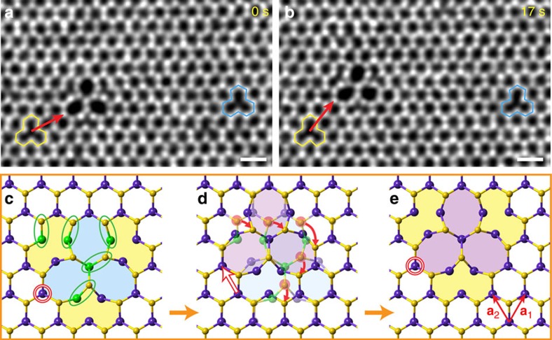
During our STEM observations, not only the Se vacancies but also the trefoil defects were mobile (Supplementary Figs 6 and 10, Supplementary Movies 3 and 4 and Supplementary Note 4). The migration rate of the trefoil defects is much lower than that of SV or DV, presumably due to the collective rearrangement of a larger number of atoms. Figure 3a,b shows an example of in-plane gliding of T1(WSe2) by one lattice constant distance (see Supplementary Movie 5). Two Se divacancies, highlighted by yellow and blue polygons, were stable in the consecutive ADF images and acted as the reference. The initial and final locations of the trefoil defect are indicated by the red arrows that point to the corners of the octagons according to the yellow divacancy. Figure 3c–e shows an atomic model of T1 defect gliding. Five pairs of W–S bonds (marked by green circles in Fig. 3c) rotate collectively clockwise (red arrows in Fig. 3d) around five W rotation centres (green atoms) to accomplish the migration of the T1 defect in a distance equal to one lattice constant in the a2 direction (red hollow arrow). Larger T2(WSe2) defects can also migrate in the host lattice (Supplementary Fig. 11, and Supplementary Movie 6) by a similar mechanism, with multiple M–X bond rotations.
Figure 3. Migration of trefoil defect in TMDs.
(a,b) T1 defect migration in WSe2. The sequential STEM images were carefully aligned according to the vicinal large cluster (not shown) using the ImageJ software. Two Se divacancies (yellow and blue polygons) are stable in the consecutive frames, and used as references. (c–e) The migration model of T1 defect glides a lattice constant distance towards the a1 direction. Scale bar, 0.5 nm.
p-type doping and magnetism of large trefoil defect and 8–5–5–8 domain boundary
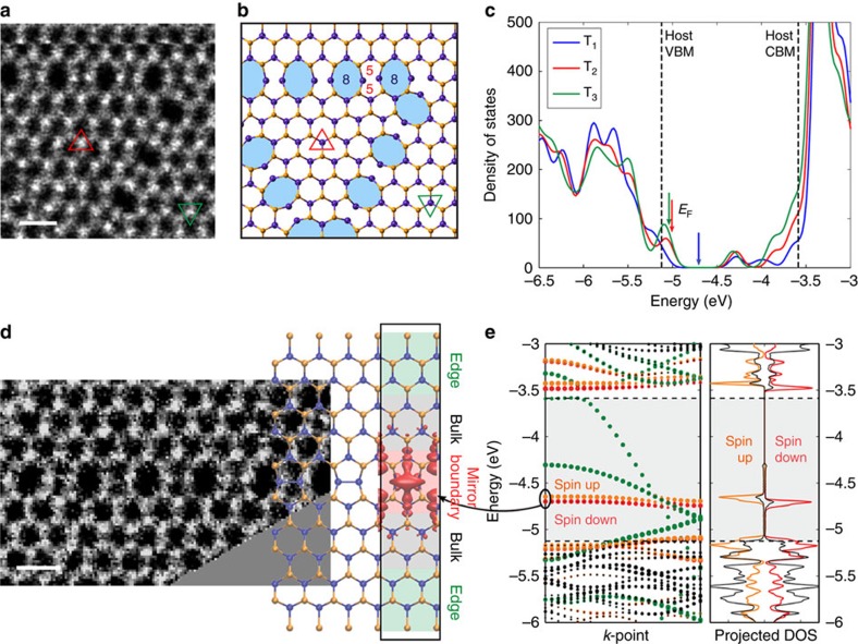
If the M–X bonds rotate further, the rotational defects can expand to even larger sizes. Figure 4a shows an ADF image of T4(WSe2) defect. According to the structural parameters for rotational defects listed in Table 1, the T4 defect involves 36 pairs of M–X bond rotation around 16 W rotation centres, which leads to a large triangular shape and each edge contains four octagons sandwiched with a pair of pentagons, as illustrated in Fig. 4b. Note that the 8–5–5–8 edges form linear domain boundaries (δ boundary), which are further visualized in Fig. 4d (extracted from the T6 defect). The calculated density of states from T1, T2, and T3 defects in WSe2 are shown in Fig. 4c. The additional states in the mid gap originate from the corners of the defect, whereas the states close to the valence band maximum and conduction band minimum can be traced to the edges (see Supplementary Figs 12 and 13). Interestingly, as the size of the defect increases, the Fermi-level moves closer to the valence band maximum, that is, the edge states of middle-sized defects essentially lead to p-type doping of the system. On the other hand, recent tight-binding transport calculations showed that the conductivity of MoS2 sheets with large rotational defects and grain boundaries containing 8–5–5–8 rings is strongly reduced across such defects21. We did not observe any rotational defects in MoS2, but their effects on the electronic transport in other TMDs we studied may be similar.
Figure 4. Large trefoil defect and magnetic 8–5–5–8 (δ) domain boundary.
(a) The ADF image of T4(WSe2). (b) The corresponding atomic model of T4(WSe2) shown in a. Larger rotational defect keep the triangular shape and include three boundaries consisting of 8–5–5–8 membered rings (δ boundary). The orientation of the inner domain of the T4 defect is 60° (or 180°) rotated from the outer domain. (c) Calculated density of states from T1 to T3 defects. The Fermi-level positions are denoted with arrows. (d) The ADF image of the boundary from T6(WSe2) with the atomic structure partially overlaid. (e) The edge band structure and density of states of the δ boundary with colours denoting projections to different regions within the ribbon geometry used in the calculation. Dashed lines denote the band edge positions of pristine WSe2. The wavefunction isosurface for the mid-gap state localized to the δ boundary is also shown in b. Energy zero is at the vacuum. Scale bar, 0.5 nm.
Table 1. Structural parameters for trefoil-like defects.
| T1 | T2 | T3 | Tn | |
|---|---|---|---|---|
| Rotation centre (Rc) for expansion | 1 | 4 | 9 |  |
| Pairs of M–X bond rotation (RP) | 3 | 10 | 21 |  |
| Octagons | 3 | 6 | 9 | 3n |
| Pentagons | 0 | 6 | 12 | 6(n-1) |
| DV(S/Se) | 3 | 5 | 7 | (2n+1) |
| Defect size (An) | 12A0 | 25A0 | 42A0 | (2n2+7n+3)A0 |
| Rc and RP for migrating a lattice constant | 5 | 9 | 13 | 4n+1 |
Unit cell size A0=9.37 Å2.
Figure 4e shows the electronic structure and the local density of states of the ideal δ boundary in WSe2. The electronic states localized to the boundary have now energies in the lower mid-gap region with very small dispersion and consequently large density of states. The conductivity along these boundaries will then strongly depend on the Fermi-level position within the gap. These states were also found to carry a magnetic moment. A similar behaviour was reported for the 5–7 dislocation22 and 8–5–5–8 boundary in MoS2 (ref. 23) and epitaxial graphene on Ni(111)24.
Discussion
Calculating the elastic properties of pristine and defective WSe2, we found that a Se vacancy concentration of 3%, in the range of the experimentally observed concentrations, decreases the bulk modulus by only about 4%. This indicates that inducing these defect structures only weakly deteriorates the mechanical properties of the system while giving rise to substantial changes in the electronic structure.
As shown in the present study by direct visualization of atomic-scale transformations, TMDs feature a rich variety of rotational defects, with the structures and their formation mechanisms related to the symmetry of the lattice but clearly distinct from those in other 2D materials such as graphene and h-BN. Phase transitions25 and inverse domains may be induced a posteriori, for example, by electron-beam irradiation, which leads to drastic changes in the material properties, for example, p-type doping and magnetism. The bond rotation mechanism reported here not only gives rise to a new class of defects, but also adds to the toolbox of available means for modifying the local properties of TMDs.
Methods
Material synthesis and sample preparation
Single crystal of MoS2, MoSe2, WS2 and WSe2 were grown by chemical vapour transport method using either Br2 as a transport agent at 950 °C. Ten grams of 99.99% purity of Mo or W, and S or Se elements with 5 mg cm−3 of Br2 were cooled in a quartz tube ampoule with liquid nitrogen and sealed in vacuum (~1 × 10⁻⁶ Torr)26,27. Single-layer TMDs were mechanically exfoliated from synthesized crystals using Scotch tape and transferred to 300 nm SiO2/Si substrate. To grow WSe2 by chemical vapour deposition, WO3 and Se powders were, respectively, used as the tungsten and selenium sources, which were placed in two separate quartz boats located in upstream of a gas flow. The temperatures of the WO3 and Se powders were set at 850 and 250 °C, respectively. The sapphire substrates where the WSe2 flakes were deposited at 750 °C were placed at the downstream side with WO3 and Se vapours being transported by an Ar/H2 flowing gas (Ar=60 s.c.c.m. and H2=3 s.c.c.m.). During the growth, the pressure of reaction chamber keeps constantly at 70 Torr. The specimens were transferred to TEM microgrid and heated in the TEM chamber (vacuum level of ~1.8 × 10⁻⁵ Pa) at 500 °C in a JEOL heating holder.
STEM-ADF-imaging experiments
STEM-ADF imaging was performed using an aberration-corrected JEOL-2100 F equipped with a DELTA corrector and cold field-emission gun. The microscope was operated at an accelerating voltage of 60 kV. The convergence semi-angle was set to 35 mrad, and the inner acquisition semi-angle was 79 mrad. The probe current was 10–15 pA. The sequential ADF images were recorded with 512 × 512 pixels and acquired with 16–64 μs dwell time. The ADF images in Figs 1, 2, 3 have been processed by low-pass filter to enhance the contrast. False-colour images and the image alignment were processed using ImageJ.
Computational details
Density functional theory calculations were carried out with the PAW method as implemented in the VASP software package28,29, using the PBE exchange-correlation functional30. The defects were modelled in periodically repeated 10 × 10 supercells of the primitive trigonal lattice with the sheets separated by 16 Å of vacuum. A single k-point was used for BZ integration and the plane-wave basis set cutoff was 300 eV. For a few selected structures, the supercell size was increased to 14 × 14 and the energy cutoff increased to 400 eV, which produced an error of at most 0.1 eV, which is our estimated numerical accuracy. Calculations for ideal boundaries were carried out in the ribbon geometry with five MX2 units on each side of the boundary and with fully chalcogen passivated edge structures, as shown in Fig. 4d. Twelve k-points along the ribbon were found to yield converged results. Robustness of the magnetization was checked by performing additional calculations with 24 k-points and of varying the smearing parameter. The results for MoSe2 look very similar to the WSe2 results.
Author contributions
F.-S.H., K.-H.L., J.J. and Y.-S.H. synthesized the MoS2, MoSe2, WS2, WSe2 single crystals by the CVT method. P.-Y.T., C.-H.Y. and P.-W.C. synthesized the single-layer WSe2 by the CVD method. Y.-C.L. and K.S. planned the project. Y.-C.L. performed the experiments and analysed the STEM data. T.B., H.-P.K. and A.V.K. performed the DFT calculations. Y.-C.L., T.B., H.-P.K., A.V.K. and K.S. co-wrote the paper. All authors discussed the results and comments on the manuscript.
Additional information
How to cite this article: Lin, Y-C. et al. Three-fold rotational defects in two-dimensional transition metal dichalcogenides. Nat. Commun. 6:6736 doi: 10.1038/ncomms7736 (2015).
Supplementary Material
Supplementary Figures 1-13, Supplementary Table 1, Supplementary Notes 1-4 and Supplementary Reference
Expansion and restoration of a trefoil defect, T0 to T1 to T2 to T0 at T=500°C.
Expansion of a trefoil defect, T2 to T3 at T=500°C.
Migration of S vacancies in MoS2 at T=500°C.
Migration of Se vacancies in WSe2 at T=500°C.
Migration of a T1 trefoil defect in WS2 at T=500°C.
Migration of a T2 trefoil defect in WSe2 at T=500°C.
Acknowledgments
Y.-C.L. and K.S. acknowledge support from JST Research Acceleration Programme. A.V.K. also acknowledges financial support from the Academy of Finland through Project No. 263416 and H.-P.K. and T.B. further thank the Academy of Finland for the support through its Centres of Excellence Programme (2012-2017) under Project No. 251748. Y.-S.H. acknowledges the support of the National Science Council of Taiwan (projects NSC 100-2112-M-011-001-MY3 and NSC 102-2811-M-011-002). P.-W.C. appreciates the project support of National Tsing Hua University and of Taiwan Ministry of Science and Technology: MOST 103-2628-M-007-004-MY3; MOST 103-2119-M-007-008-MY3; and MOST 102-2633-M-007-002- (P.-W.C.). We also thank CSC-IT Center for Science Ltd. for generous grants of computer time.
References
- Suenaga K. et al. Imaging active topological defects in carbon nanotubes. Nat. Nanotechnol. 2, 358–360 (2007) . [DOI] [PubMed] [Google Scholar]
- Robertson A. W. et al. Stability and dynamics of the tetravacancy in graphene. Nano Lett. 14, 1634–1642 (2014) . [DOI] [PubMed] [Google Scholar]
- Kotakoski J., Krasheninnikov A. V., Kaiser U. & Meyer J. C. From point defects in graphene to two-dimensional amorphous carbon. Phys. Rev. lett. 106, 105505 (2011) . [DOI] [PubMed] [Google Scholar]
- Stone A. J. & Wales D. J. Theoretical studies of icosahedral C60 and some related species. Chem. Phys. Lett. 128, 501–503 (1986) . [Google Scholar]
- Banhart F., Kotakoski J. & Krasheninnikov A. V. Structural defects in graphene. ACS Nano 5, 26–41 (2011) . [DOI] [PubMed] [Google Scholar]
- Lee G. D. et al. Diffusion, coalescence, and reconstruction of vacancy defects in graphene layers. Phys. Rev. Lett. 95, 205501 (2005) . [DOI] [PubMed] [Google Scholar]
- Warner J. H. et al. Dislocation-driven deformations in graphene. Science 337, 209–212 (2012) . [DOI] [PubMed] [Google Scholar]
- Lehtinen O., Kurasch S., Krasheninnikov A. V. & Kaiser U. Atomic scale study of the life cycle of a dislocation in graphene from birth to annihilation. Nat. Commun. 4, 1–7 (2013) . [DOI] [PubMed] [Google Scholar]
- Warner J. H. et al. Rippling graphene at the nanoscale through dislocation addition. Nano Lett. 13, 4937–4944 (2013) . [DOI] [PubMed] [Google Scholar]
- Kurasch S. et al. Atom-by-atom observation of grain boundary migration in graphene. Nano Lett. 12, 3168–3173 (2012) . [DOI] [PubMed] [Google Scholar]
- Meyer J. C., Chuvilin A., Algara-Siller G., Biskupek J. & Kaiser U. Selective sputtering and atomic resolution imaging of atomically thin boron nitride membranes. Nano Lett. 9, 2683–2689 (2009) . [DOI] [PubMed] [Google Scholar]
- Jin C., Lin F., Suenaga K. & Iijima S. Fabrication of a freestanding boron nitride single layer and its defect assignments. Phys. Rev. Lett. 102, 195505 (2009) . [DOI] [PubMed] [Google Scholar]
- Cretu O., Lin Y. C. & Suenaga K. Evidence for active atomic defects in monolayer hexagonal boron nitride: a new mechanism of plasticity in two-dimensional materials. Nano Lett. 14, 1064–1068 (2014) . [DOI] [PubMed] [Google Scholar]
- Gibb A. I. et al. Atomic resolution imaging of grain boundary defects in monolayer chemical vapor deposition-grown hexagonal boron nitride. J. Am. Chem. Soc. 135, 6758–6761 (2013) . [DOI] [PubMed] [Google Scholar]
- Zhou W. et al. Intrinsic structural defects in monolayer molybdenum disulfide. Nano Lett. 13, 2615–2622 (2013) . [DOI] [PubMed] [Google Scholar]
- van der Zande A. M. et al. Grains and grain boundaries in highly crystalline monolayer molybdenum disulphide. Nat. Mater. 12, 554–561 (2013) . [DOI] [PubMed] [Google Scholar]
- Komsa H. P. et al. Two-dimensional transition metal dichalcogenides under electron irradiation: defect production and doping. Phys. Rev. Lett. 109, 035503 (2012) . [DOI] [PubMed] [Google Scholar]
- Komsa H. P., Kurasch S., Lehtinen O., Kaiser U. & Krasheninnikov A. V. From point to extended defects in two-dimensional MoS2: evolution of atomic structure under electron irradiation. Phys. Rev. B 88, 035301 (2013) . [Google Scholar]
- Najmaei S. et al. Vapor phase growth and grain boundary structure of molybdenum disulphide atomic layers. Nat. Mater. 12, 754–759 (2013) . [DOI] [PubMed] [Google Scholar]
- Liu Z. et al. Identification of active atomic defects in a monolayered tungsten disulphide nanoribbon. Nat. Commun. 2, 1–5 (2011) . [DOI] [PubMed] [Google Scholar]
- Ghorbani-Asl M., Enyashin A. N., Kuc A., Seifert G. & Heine T. Defect-induced conductivity anisotropy in MoS2 monolayers. Phys. Rev. B 88, 245440 (2013) . [Google Scholar]
- Zhang Z., Zou X., Crespi V. H. & Yakobson B. I. Intrinsic magnetism of grain boundaries in two-dimensional metal dichalcogenides. ACS Nano 7, 10475–10481 (2013) . [DOI] [PubMed] [Google Scholar]
- Enyashin A. N., Bar-Sadan M., Houben L. & Seifert G. Line defects in molybdenum disulfide layers. J. Phys. Chem. C 117, 10842–10848 (2013) . [Google Scholar]
- Lahiri J., Lin Y., Bozkurt P., Oleynik I. I. & Batzill M. An extended defect in graphene as a metallic wire. Nat. Nanotechnol. 5, 326–329 (2010) . [DOI] [PubMed] [Google Scholar]
- Lin Y. C., Dumcenco D. O., Huang Y. S. & Suenaga K. Atomic mechanism of the semiconducting-to-metallic phase transition in single-layered MoS2. Nat. Nanotechnol. 9, 391–396 (2014) . [DOI] [PubMed] [Google Scholar]
- Tiong K. K., Huang Y. S. & Ho C. H. Electrical and optical anisotropic properties of rhenium-doped molybdenum disulphide. J. Alloy. Compd 317–318, 208–212 (2001) . [Google Scholar]
- Dumcenco D. O. et al. Optical properties of tungsten disulfide single crystals doped with gold. Mater. Chem. Phys. 111, 475–479 (2008) . [Google Scholar]
- Kresse G. & Furthmuller J. Efficiency of ab-initio total energy calculations for metals and semiconductors using a plane-wave basis set. Comput. Mater. Sci. 6, 15–50 (1996) . [DOI] [PubMed] [Google Scholar]
- Kresse G. & Joubert D. From ultrasoft pseudopotentials to the projector augmented-wave method. Phys. Rev. B 59, 1758–1775 (1999) . [Google Scholar]
- Perdew J. P., Burke K. & Ernzerhof M. Generalized gradient approximation made simple. Phys. Rev. Lett. 77, 3865–3868 (1996) . [DOI] [PubMed] [Google Scholar]
Associated Data
This section collects any data citations, data availability statements, or supplementary materials included in this article.
Supplementary Materials
Supplementary Figures 1-13, Supplementary Table 1, Supplementary Notes 1-4 and Supplementary Reference
Expansion and restoration of a trefoil defect, T0 to T1 to T2 to T0 at T=500°C.
Expansion of a trefoil defect, T2 to T3 at T=500°C.
Migration of S vacancies in MoS2 at T=500°C.
Migration of Se vacancies in WSe2 at T=500°C.
Migration of a T1 trefoil defect in WS2 at T=500°C.
Migration of a T2 trefoil defect in WSe2 at T=500°C.


