Abstract
Atomically defined substrate surfaces are prerequisite for the epitaxial growth of complex oxide thin films. In this protocol, two approaches to obtain such surfaces are described. The first approach is the preparation of single terminated perovskite SrTiO3 (001) and DyScO3 (110) substrates. Wet etching was used to selectively remove one of the two possible surface terminations, while an annealing step was used to increase the smoothness of the surface. The resulting single terminated surfaces allow for the heteroepitaxial growth of perovskite oxide thin films with high crystalline quality and well-defined interfaces between substrate and film. In the second approach, seed layers for epitaxial film growth on arbitrary substrates were created by Langmuir-Blodgett (LB) deposition of nanosheets. As model system Ca2Nb3O10- nanosheets were used, prepared by delamination of their layered parent compound HCa2Nb3O10. A key advantage of creating seed layers with nanosheets is that relatively expensive and size-limited single crystalline substrates can be replaced by virtually any substrate material.
Keywords: Chemistry, Issue 94, Substrates, oxides, perovskites, epitaxy, thin films, single termination, surface treatment, nanosheets, Langmuir-Blodgett
Introduction
Lots of research is performed on epitaxial thin films and heterostructures of complex oxides because of the wide range of functional properties that can be obtained by tuning the composition and structure of the materials. Due to the development of several growth techniques, nowadays it is possible to make a large range of films with compositions and crystalline qualities that cannot be reached in bulk.1 Together with the fact that the properties of these materials are highly anisotropic, this makes that in epitaxial films phenomena and functionalities are observed that are not obtained in bulk. Besides, epitaxial strain and the creation of heterostructures can be used to obtain new or enhanced properties.2
In order to grow epitaxial films and heterostructures with the desired properties, substrates with well-defined surfaces are required. Local differences in surface chemistry or morphology cause inhomogeneous nucleation and growth, which gives rise to undesired defects and grain boundaries in the film. Furthermore, the interface between film and substrate plays an important role in determining the properties because of the limited thickness of the film. This means that substrates are required that are smooth and homogeneous on the atomic level.
This criterion is hard to reach when substrates are used that naturally do not have well-defined surfaces, e.g., other complex oxides. From this perspective, perovskite oxides are one of the most studied substrate materials. Perovskite oxides can be represented by the general formula ABO3, in which A and B stand for metal ions. Almost all metals can be incorporated in the A or B site, which makes it possible to fabricate a wide range of different substrates. The versatility of the substrate material allows one to tune the properties of the film grown on top of it by tuning the applied epitaxial strain and the structure at the interface. However, growth on these substrates is not straightforward due to the ambiguous nature of the perovskite surface, which is especially visible in (001) oriented substrates. In the (001) direction, perovskites can be seen as alternating layers of AO and BO2. When a (001) oriented substrate is made by cleaving from a larger crystal, both oxides are present at the surface. This phenomenon is shown in Figure 1. Since the crystal is never perfectly cleaved along the (001) plane, a surface forms consisting of terraces with unit cell height differences. However, height differences of half a unit cell exist as well, which indicates the presence of both types of surface terminations. It is important to have single terminated perovskite substrates in order to grow a continuous film with homogeneous properties, as has been shown especially for the growth of perovskite oxide films. The termination can cause a large difference in growth kinetics, leading to growth of non-continuous films.3–5 Furthermore, the stacking order should be similar across the complete film-substrate interface, since AO-B’O interfaces can have totally different properties than BO-A’O interfaces.6
The first successful method to obtain a single terminated perovskite oxide surface was developed for SrTiO3 (001) oriented substrates. Kawasaki et al.7 introduced a wet etching method, which was later ameliorated by Koster et al.8 The method consists of increasing the sensitivity of the SrO towards acidic etching by hydroxylating this oxide in water, followed by a short etch in buffered hydrogen fluoride (BHF). Subsequent annealing to increase the crystallinity yields an atomically smooth surface were only TiO2 is present. Later, a method to obtain single terminated rare earth scandates was developed by using the higher solubility of rare earth oxides compared to scandates in basic solution. This method was especially described for the orthorhombic (110) oriented DyScO3, and it was shown that it is possible to obtain completely scandate terminated surfaces.9,10 The methods to obtain these single terminated SrTiO3 and DyScO3 substrates are described in this protocol.
Though the value of single crystalline perovskite substrates is clear, alternatively, arbitrary substrates without suitable crystal structures can be used for epitaxial film growth as well. Substrates that are unsuitable for epitaxial film growth by themselves can be made into suitable templates by covering them with a layer of nanosheets. Nanosheets are essentially two-dimensional single crystals, with a thickness of a few nanometers and a lateral size in the micrometer range11, and thus possess the ability to direct epitaxial growth of thin films. By depositing a layer of nanosheets on an arbitrary substrate, a seed layer is created for oriented growth of any film material with matching lattice parameters. This approach has been reported successful for the oriented growth of for example ZnO, TiO2, SrTiO3, LaNiO3, Pb(Zr,Ti)O3 and SrRuO3.12–15 By using nanosheets, the relatively high prices and size limitations of regular single crystalline substrates can be avoided and nanosheets can be deposited on virtually any substrate material.
Nanosheets are generally obtained by delamination of a layered parent compound into its discrete layers, with their specific thickness determined by the crystal structure of the parent compound.11 Delamination can be achieved in aqueous environment by exchanging the interlayer metal ions in the parent compound with bulky organic ions, which causes the structure to swell and ultimately delaminate into unilamellar nanosheets. This results in a colloidal dispersion of charged nanosheets that are surrounded by counter-charged organic ions. A schematic representation of the delamination process is shown in Figure 2. In the present protocol, Ca2Nb3O10- nanosheets were used as a model system and these can be obtained from the perovskite parent compound HCa2Nb3O10. Ca2Nb3O10- nanosheets have in-plane lattice parameters almost equal to those of SrTiO3 and display an atomically smooth, single terminated surface. Therefore, high quality films can be grown on individual nanosheets. Once an aqueous dispersion of nanosheets is obtained, they can be deposited on an arbitrary substrate by Langmuir-Blodgett (LB) deposition. This method enables nanosheet deposition in monolayers with a high controllability that generally cannot be achieved by other conventional techniques like electrophoretic deposition or flocculation.11 The organic ions surrounding the nanosheets are surface-active molecules and tend to diffuse to the surface of the dispersion, creating a monolayer of floating nanosheets. This monolayer can be compressed into dense packing and deposited onto an arbitrary substrate. A schematic representation of the deposition process is shown in Figure 3; a surface coverage of over 95% is generally achievable15–18 and this occurs mainly without stacking of nanosheets or overlapping edges. Multilayers can be obtained by repeated deposition.
In the present protocol Ca2Nb3O10- nanosheets were used as a model system, but the principle of using nanosheets as a seed layer for epitaxial film growth is more widely applicable. Though oxide nanosheets receive more attention as seed layers in literature, the concept may be extended to non-oxide nanosheets such as BN, GaAs, TiS2, ZnS and MgB2as well. Furthermore, since nanosheets inherit the composition of their parent compound, various functionalities can be inserted by appropriate design of the parent structure. In addition to their use as seed layer for oriented film growth, a wide variety of nanosheets has proven to be a valuable toolbox in studying fundamental material properties and engineering new functional structures.11,19–22
This protocol shows the experimental procedures to obtain the different types of templates for epitaxial growth oxide thin films. The complete procedures to obtain well-defined single terminated SrTiO3 and DyScO3 substrates are described, as well as the procedure to fabricate Ca2Nb3O10- nanosheet layers on arbitrary of substrates.
Protocol
1. Atomically Smooth, Singly Terminated Surfaces
- Cleaning SrTiO3 and DyScO3 substrates
- Immerse the substrates in a beaker filled with acetone (purity 99.5%) and place it in an ultrasonic bath (UB) for 10 min. Repeat this step with ethanol (purity 99.8%), without drying the substrate in between. Use a nitrogen gun to dry the samples by blowing the ethanol drops from the surface. In this way, particles that are present in ethanol will not stay on the surface after drying.
- Check the surface with an optical microscope. Remove any leftover particles by rubbing the substrate gently on a lens tissue, which is soaked in ethanol. Always use a nitrogen gun to dry the sample. Repeat step 1.1.1 and 1.1.2 until the surface is free from particles.
- DyScO3 treatment — annealing
- Load the cleaned substrates in a quartz boat and anneal them in a clean tube oven at 1,000 °C in flowing oxygen (150 ml/hr) for 4 hr.
- Check the surface with an optical microscope. If dirt is visible, use the procedure described in step 1.1.2 to clean the surface.
- DyScO3 treatment — surface roughening by BHF
- Immerse the clean substrates in a 100 ml beaker containing 40 ml deionized (DI) water and place it in an UB for 30 min. Use a Teflon holder to carry the substrates.
- Fill three HF resistant 100 ml beakers with 40 ml DI water. Fill one 100 ml beaker with 40 ml of ethanol. Fill one HF resistant beaker with 40 ml 12.5% buffered hydrogen fluoride (BHF, NH4F:HF = 87.5:12.5, pH = 5.5). NOTE: BHF is a very dangerous acid. Proper precautions should be taken.
- Transfer the Teflon holder carrying the substrates from the beaker with DI water to the beaker containing BHF. Put the beaker in the UB for 30 sec.
- Transfer the Teflon holder to an HF resistant beaker containing DI water and immerse for 20 sec, gently moving the holder up and down. Repeat this in the two other beakers filled with water. Leave the holder with samples in the beaker containing ethanol.
- Dispose of all BHF containing liquid.
- Dry the substrates using a nitrogen gun. Check the surface with an optical microscope. If dirt is visible, repeat step 1.1.2.
- DyScO3 treatment — selective etching by NaOH
- Fill a 100 ml beaker with 40 ml 12 M NaOH (aq). Immerse the samples using a Teflon holder and place the beaker in an UB for 30 min.
- Transfer the samples to a 100 ml beaker containing 40 ml 1 M NaOH (aq). Put it in the UB for 30 min.
- Fill three beakers with DI water and one beaker with ethanol. Rinse the samples by subsequent immersing in the three beakers with water and finally in the beaker with ethanol. Dry the samples using a nitrogen gun.
- Check the surface with an optical microscope and clean if necessary, using the procedure described in step 1.1.2. The DyScO3 samples are singly terminated now.
- SrTiO3 treatment
- Etch the cleaned substrates using BHF as described in step 1.3. Note that, while this step is used for DyScO3 just as a surface roughening step, the selective etching of SrO occurs in this step.
- Anneal the samples at 950 °C in flowing oxygen (150 ml/hr) for 90 min. The SrTiO3 samples are singly terminated now. Check the surface with an optical microscope and clean if necessary, using the procedure described in step 1.1.2.
2. Atomically Defined Templates on Arbitrary Substrates
- Preparation of Ca2Nb3O10- nanosheets
- Make a dispersion of HCa2Nb3O10 powder in DI water with a concentration of 0.40 g/100 ml and add an equimolar amount of tetra-butyl ammonium hydroxide (TBAOH). Please refer to Ebina et al.23 for the solid-state synthesis of KCa2Nb3O10 powder and its protonation to HCa2Nb3O10. NOTE: TBAOH is corrosive; wear gloves at all times and handle with care.
- Gently shake the bottle by hand and place it horizontally on a rocking shaker at 30 Hz for 14 days. Re-disperse the precipitation five to six times during these 14 days by slowly rolling the bottle.
- Dilute the dispersion to 0.40 g/L and gently shake it again. Let it stand for at least 24 hr before use in order to let large aggregates settle to the lower part of the dispersion. NOTE: The batch size may affect the process. Here, initial batches of 100 ml and diluted batches of 500 ml were made, both in polypropylene bottles.
- Deposition of Ca2Nb3O10 nanosheets NOTE: Various versions of equipment and software yield various operational settings. Please refer to the manual of the setup for all options.
- Clean the Wilhelmy plate by rinsing with DI water and cleaning with oxygen plasma at high energy for at least 3 min for each side. Store the Wilhelmy plate in DI water immediately afterwards. NOTE: If multiple depositions are done successively, the Wilhelmy plate does not need to be treated with oxygen plasma every time.
- Clean the Langmuir-Blodgett trough and the two barriers by rinsing with DI water, brushing with ethanol, again rinsing with DI water and drying with nitrogen gas. Make sure the setup is placed on an anti-vibration table to protect against vibrations, and in a box that can be closed during deposition to protect against flowing air and dust.
- Take 50 ml from the upper part of a fresh nanosheet dispersion with a syringe and slowly put it in the trough. Make sure the edges of the trough and the barriers are free of droplets. NOTE: The amount required for one deposition depends on the size of the trough. The water surface must be slightly higher than the edges of the trough, to make sure that the barriers can compress the surface properly.
- Let the dispersion rest for 15 min.
- Choose an arbitrary substrate compatible with aqueous solutions and clean it properly. Attach the substrate to the holder of the LB setup and give it a final blow with nitrogen gas. NOTE: Keep in mind that atomically flat films have to be grown on atomically flat substrates. Example data in this report were obtained with silicon substrates, which were cleaned with ethanol, a jet of supercritical CO2 for 30 sec and oxygen plasma at high energy for 5 min.
- Attach the substrate holder to the setup. Take the Wilhelmy plate, dip it in the trough and carefully attach it to the spring. Remove droplets from the wire of the plate with a piece of paper.
- Lower the substrate until it touches the surface of the nanosheet dispersion, set the height in the software to zero and lower the substrate further until the desired depth. Make sure that the substrate holder does not touch the nanosheet dispersion.
- Set the surface pressure in the software to zero and let the dispersion rest for 15 min. After 15 min the surface pressure typically reaches 1 to 2 mN/m. Large deviations may indicate poor quality of the following deposition.
- Set the surface pressure in the software to zero again and start the first stage of the deposition by moving the barriers with a rate of 3.0 mm/min to slowly compress the surface. Make sure that the value of the target pressure in the software is well above the maximum value expected in step 2.2.10 (i.e., 20 mN/m).
- Monitor the development of surface pressure and surface area. Wait until the increase of the pressure slows down significantly and the pressure approaches its maximum. Make sure the barriers never reach the Wilhelmy plate. The maximum pressure typically reaches 15.0 to 18.0 mN/m, but this is neither an absolute nor a constant value.
- Enter the reached value as target pressure, set the dipper height to the actual value and start the second stage of the deposition by withdrawing the substrate from the dispersion with a rate of 1.0 mm/min. Monitor the surface pressure.
- Remove the Wilhelmy plate when the deposition is finished, rinse it with DI water and store it in DI water again.
- Remove the substrate after it has dried completely.
- For multilayer deposition, decompose the organic residues from the previous layer. This can be done for example by heating to 600 °C in a microwave oven for 30 min or by ultraviolet irradiation for 30 min. Repeat the protocol from step 2.2.2, but do not clean the substrate other than with a blow of nitrogen gas.
Representative Results
Step 1) Selective etching of SrTiO3 and DyScO3 substrates
Atomic force microscopy (AFM) is a straightforward way to obtain an indication about the success of the treatment. The AFM image of an SrTiO3 substrate which had only been flashed to 650 °C (Figure 4A) shows a rough surface, demonstrating the necessity of a high temperature annealing step. The AFM data of an annealed substrate (Figures 4A-C) clearly show two surface terminations, since clear contrast in the friction image is observed, as well as half unit cell height differences in a cross section of the height image. Figure 5 shows AFM images of TiO2 terminated SrTiO3 substrates, which were treated according to the method described in this protocol. On large scale, straight terrace ledges can be observed (Figure 5A). On smaller scale, very smooth terraces are observed, and only unit cell height differences between the terraces are measured, as expected for single terminated surfaces. On substrates with larger terraces, i.e., with smaller miscut angles, unit cell deep holes are visible near the terrace ledges (Figure 5B). These holes disappear when longer annealing times are used, leading to morphologies similar to single terminated substrates with higher miscut angles (Figure 5C). The morphology of these holes, as well as the morphology of the terrace ledges, are an important indication of single termination.24 On single terminated substrates, the holes are circular shaped, while the terrace ledges are rounded. In contrast, sharp-edged terrace ledges and square holes are visible on double terminated substrates (see Figure 4B).
Another indication of single termination appears in reflection high-energy electron diffraction (RHEED) images, as shown in Figure 6. In RHEED images of as received substrates, streaks appear due to poor crystallinity of the surface. After annealing in oxygen or full treatment of the substrate, the surface is more ordered, as can be seen by the appearance of Kikuchi lines and sharp diffraction spots. However, in the case of single terminated substrates, the diffraction spots are even smaller compared to substrates that are only annealed. More important, besides the (1x1) spots, no additional spots are visible, which are always present in patterns of double terminated substrates
In the case of DyScO3, it is more difficult to see whether or not a treatment is successful. No differences can be seen between RHEED patterns of annealed double terminated substrates and chemically treated ScO2 terminated substrates.10 In Figure 7, AFM images of different annealed DyScO3 substrates are shown. Different terminations can easily be seen in Figure 7A-D. Figure 7E and F show the morphology expected for single terminated substrates, i.e. only 4 Å steps are visible. However, the mixed termination can still occur at very small scale. Due to the limited resolution of the AFM, the areas of different terminations are not clearly visible. Higher surface roughness in both height and phase images compared to single terminated surfaces are an indication of the presence of both terminations.
Scanning probe microscopy and surface diffraction techniques are not sufficient to completely determine the success of a treatment. Minor regions of the second termination may not be observed with both types of techniques due to limited resolution. However, these minor regions can have a dramatic influence on the quality of the film, as shown in Figure 8. The nucleation of SrRuO3 is very sensitive towards surface termination.3–5 Although the AFM images of the DyScO3 and SrTiO3 substrates in respectively Figure 8C and F seemed to show single terminated surfaces, growth of SrRuO3 shows that regions of the other termination were still present. In the end, the success of a treatment can only be fully determined considering the quality of the grown film.
Step 2) Deposition of Ca2Nb3O10- nanosheets on arbitrary substrates
During nanosheet deposition, the change in surface pressure can be monitored and this gives an indication on how the deposition proceeds. Typical plots of the surface pressure during the initial surface area compression and the actual deposition of nanosheets are shown in Figure 9. The pressure generally increases for an increasingly dense packing of floating nanosheets and increases more rapidly as the packing density approaches 100%. The actual deposition should start just before the surface pressure reaches its maximum and this pressure will be maintained throughout the deposition. In case the pressure passes its maximum and (slightly) collapses, this could indicate that the high compressing force caused the edges of some nanosheets to overlap each other and create (partial) stacks. As long as the pressure does not approach a maximum, the nanosheets are not yet organized into a dense packing. During the actual deposition, the barriers slowly move back and forth to enable local reorganization of the nanosheet monolayer and this causes a saw-like pressure profile.
A typical AFM image of a monolayer of nanosheets is shown in Figure 10. The nanosheet surfaces are smooth and the height difference with adjacent gaps approaches the 1.44 nm crystallographic thickness of Ca2Nb3O10- layers in their parent compound11. A monolayer of nanosheets is fully (001) oriented in the out-of-plane direction, but has a random in-plane orientation due to the random in-plane ordering of nanosheets. To illustrate their crystal orientations and quality, Figure 11 shows an electron backscatter diffraction (EBSD) image of epitaxial SrRuO3 grown on Ca2Nb3O10- nanosheets with an intermediate layer of SrTiO3. The film has an out-of-plane (001) orientation on all nanosheets and has a single in-plane orientation on individual nanosheets. The surface morphology of such films is illustrated with the AFM image in Figure 12.The step heights in the continuous parts correspond either with the nanosheet thickness or with the unit cell height of SrRuO3, confirming high quality film growth on atomically perfect nanosheets. For an extended report on the properties of epitaxial SrRuO3 films grown by this approach, please refer to Nijland et al.15
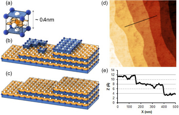 Figure 1. (A) Schematic representation of a cubic perovskite unit cell. The metal ions A and B are located in, respectively, the corners and center of the unit cell. The oxygen atoms are located at the faces of the cube, forming an octahedron around the B ion. (B) Schematic representation of a (001) oriented perovskite substrate. Due to a miscut, the surface consists of terraces. Both terminations, AO and BO2, are present at the surface. (C) Schematic representation of a completely BO2 terminated substrate. (D) AFM image of the surface of a DyScO3 substrate after annealing at 1,000 °C for 4 hr. The roughness on the terraces is caused by the presence of two surface terminations, as shown in the line profile (E), where not only the 4 Å unit cell steps, but also 2 Å height differences are visible. Figures A-C are adapted from Kleibeuker et al.9
Please click here to view a larger version of this figure.
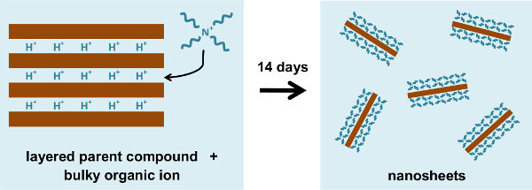 Figure 2. Schematic representation of the delamination of a layered parent compound into unilamellar nanosheets. Ion exchange with bulky molecules causes the structure to swell and reduces the interlayer electrostatic forces, allowing the layers to be separated from each other. Please click here to view a larger version of this figure.
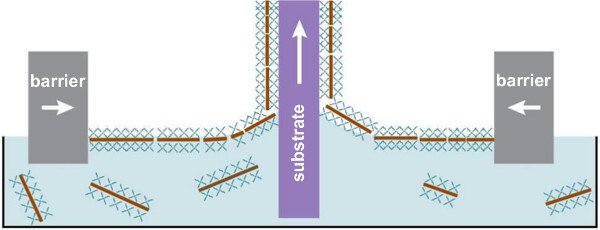 Figure 3. Schematic representation of nanosheet deposition by the LB method. The nanosheets float towards the surface of the dispersion and are compressed into a dense packing by the barriers moving inward. The substrate is then slowly withdrawn from the dispersion. Please click here to view a larger version of this figure.
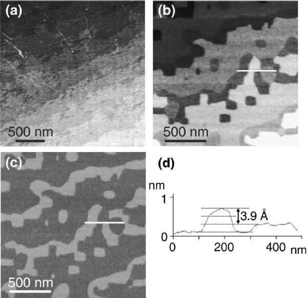 Figure 4. (A) AFM image of an SrTiO3 substrate which had been flashed to 650 °C. (B) AFM height and (C) friction image of a double terminated SrTiO3 substrate, showing sharp step edges and terraces with half a unit cell height difference compared to the adjacent terraces, as visible in the line profile of the AFM height image shown in (D). The two different terminations cause a clear contrast in the friction image. Figure taken with permission from Koster et al.8
Please click here to view a larger version of this figure.
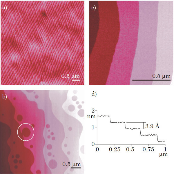 Figure 5. (A-C) AFM images of single terminated SrTiO3 substrates. (D) is a line profile of (C), showing only unit cell height differences. The circle in (B) indicates one of the unit cell deep holes which are visible near the terrace ledges of substrates with low miscut angles. Figure taken with permission from Koster et al.24
Please click here to view a larger version of this figure.
 Figure 6. RHEED images of (A) an as received SrTiO3 substrate, (B) an annealed substrate and (C) a single terminated SrTiO3 substrate. Figure taken with permission from Koster et al.24
Please click here to view a larger version of this figure.
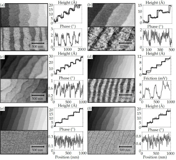 Figure 7. AFM images of annealed DyScO3 substrates.(A-D) show clearly double terminated surfaces. However, the morphology can vary from substrate to substrate. The surfaces of (E) and (F) look more homogenous, and only unit cell height differences can be measured. However, the resolution of the AFM can be too low to measure small areas of a second termination25. Please click here to view a larger version of this figure.
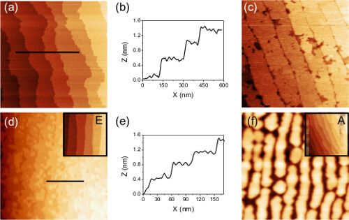 Figure 8.AFM images of SrRuO3 films grown on SrTiO3 and DyScO3 substrates. The films in (A) and (D) are grown on respectively SrTiO3 and DyScO3 substrates which were treated according to the methods described in this protocol. The films are very smooth, and the corresponding line profiles shown in (B) and (E) show only unit cell height differences. The films in (C) and (F) were grown on double terminated annealed substrates. Trenches are visible which are in the range of the film thickness. The insets in (D) and (F) show the substrate before growth. Note that both surfaces are very smooth. Figure taken with permission from Kleibeuker et al.9
Please click here to view a larger version of this figure.
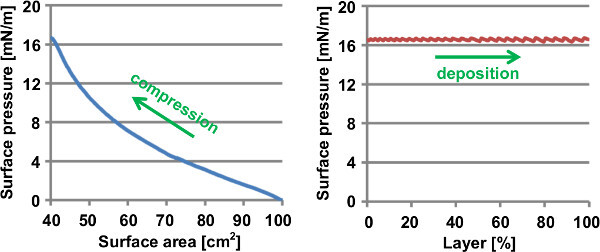 Figure 9. Typical plots of the surface pressure during the initial surface area compression and the actual deposition of Ca2Nb3O10- nanosheets.
Please click here to view a larger version of this figure.
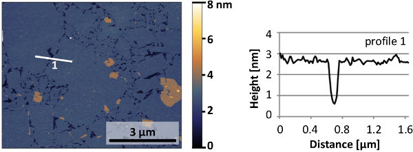 Figure 10. Typical AFM image and line profile of a monolayer of Ca2Nb3O10- nanosheets deposited on a silicon substrate. The nanosheets display smooth surfaces. Please click here to view a larger version of this figure.
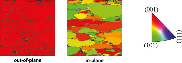 Figure 11.EBSD image of epitaxial SrRuO3grown on Ca2Nb3O10- nanosheets with an intermediate layer of SrTiO3. The film has an out-of-plane (001) orientation on all nanosheets and has a single in-plane orientation on individual nanosheets. Please click here to view a larger version of this figure.
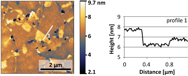 Figure 12. AFM image and line profile of epitaxial SrRuO3 grown on Ca2Nb3O10- nanosheets with an intermediate layer of SrTiO3. Step heights in the continuous parts match the nanosheet thickness of 1.4 nm and the SrRuO3 unit cell height of 0.4 nm. Please click here to view a larger version of this figure.
Discussion
The most important aspect of all perovskite oxide substrate treatments is the cleanliness of the work. Surface contaminations prevent etching of areas of the substrate, while unwanted reactions during annealing can easily damage the surface.
The order of the different steps is important as well. In the treatment of DyScO3, the annealing step should be performed before the etching step, since post-annealing leads to unwanted Dy diffusion from the bulk to the surface of the substrate. After etching in the 12 M NaOH solution, a 1 M solution should always be used in order to prevent precipitation of dysprosium hydroxide complexes onto the substrate surface. Soaking in water is necessary for the SrTiO3 treatment in order to hydroxylize the SrO. In this way, short etching times can be used which prevents damaging of the surface due to uncontrolled etching. Immersing in water is an optional step in case of the DyScO3 treatment. This step is simply copied from the standardized SrTiO3 treatment procedure and is not expected to have any significance in the treatment.
The annealing steps are necessary to improve the crystallinity of the surface. The indicated annealing times for DyScO3 and SrTiO3 treatments are times that, on average, lead to well defined step ledges. However, sometimes the annealing time needs to be increased for substrates with a low miscut angle, i.e., with wider terraces. An increased diffusion length is then required for the surface atoms to find the optimal sites. In the case of SrTiO3, a too long annealing time may cause unwanted diffusion of Sr atoms from the bulk to the surface. This second termination can be observed in the surface morphology by appearance of straight step edges and square holes, as described in the section on representative results. In that case, the surface treatment can be repeated, but the final annealing step should be performed at 920 °C for 30 min26.
The methods described in this protocol are the most successful methods for (001) SrTiO3 and rare earth scandates, but are applicable to these substrates only. However, methods for other substrates should be adjusted to the exact surface chemistry. This is also required when substrates with other orientations are used, or when A-site instead of B-site termination is desired. An overview of existing treatments can be found in Sánchez et al.6 and Schlom et al.2
Regarding seed layers of nanosheets, delicate parts of the process are to obtain high quality nanosheet dispersions and to prevent contamination during the deposition. Delamination of a layered parent compound into unilamellar nanosheets by addition of bulky organic ions occurs readily, but nanosheets tend to aggregate in dispersion and such aggregates will hinder the deposition of homogeneous monolayers. Therefore, it is very important to leave a freshly diluted dispersion at rest for at least 24 hr before use and not to use the lower part of the dispersion. This leaves time for large aggregates to settle and the upper part of the dispersion will become relatively pure. Since ongoing aggregation will continuously degrade the dispersion, use within one week after dilution is recommended. Please note that the occurring gradient in nanosheet concentration throughout the dispersion volume causes some variations in the surface pressure values during LB deposition, depending on the local nanosheet concentration in the volume taken from the stock dispersion. Furthermore, LB deposition is based on surface-active molecules and thus is very sensitive to contaminations and movement. Careful cleaning of the setup and Wilhelmy plate (preferably with cleaning tools dedicated to this setup only) and protection against flowing air and vibrations are very important.
The concept of creating a seed layer of nanosheets on arbitrary substrates by LB deposition is a valuable tool in the field of thin film growth. The atomically perfect surface of nanosheets yields high quality epitaxial films of, in principle, any film material with matching lattice parameters. Nanosheets can be deposited on virtually any substrate material and thus other materials can replace relatively expensive and size-limited single crystalline substrates. The LB method enables nanosheet deposition in monolayers with a high controllability that generally cannot be achieved by other conventional techniques like electrophoretic deposition or flocculation.11 However, the bottleneck is in the degree of perfection of the seed layer. High film qualities over large areas are required for reliable application in functional devices and to date, this has not been achieved. To deposit nanosheets with a perfect coverage and preferably also to control their in-plane orientation are main challenges in the field. Nevertheless, the current state of the art has already proven to be a valuable tool in research.
Disclosures
The authors declare that they have no competing financial interests.
Acknowledgments
This work is financially supported by the Netherlands Organization for Scientific Research (NWO) through a VIDI grant and by the Chemical Sciences division of the Netherlands Organization for Scientific Research (NWO-CW) in the framework of the TOP and ECHO programs.
References
- Schlom DG, Chen L-Q, Pan X, Schmehl A, Zurbuchen MA. A Thin Film Approach to Engineering Functionality into Oxides. J. Am. Ceram. Soc. 2008;91(8):2429–2454. [Google Scholar]
- Schlom DG, Chen L-Q, et al. Elastic strain engineering of ferroic oxides. MRS Bulletin. 2014;39(2):118–130. [Google Scholar]
- Rijnders G, Blank DHA, Choi J, Eom C-B. Enhanced surface diffusion through termination conversion during epitaxial SrRuO3 growth. Appl. Phys. Lett. 2004;84(4):505. [Google Scholar]
- Bachelet R, Sánchez F, Santiso J, Munuera C, Ocal C, Fontcuberta J. Self-Assembly of SrTiO3 (001) Chemical-Terminations: A Route for Oxide-Nanostructure Fabrication by Selective Growth. Chem. Mater. 2009;21(12):2494–2498. [Google Scholar]
- Kuiper B, Blok JL, Zandvliet HJW, Blank DHA, Rijnders G, Koster G. Self-organization of SrRuO3 nanowires on ordered oxide surface terminations. MRS Communications. 2011;1(1) [Google Scholar]
- Ocal C, Fontcuberta J. Tailored surfaces of perovskite oxide substrates for conducted growth of thin films. Chem Soc Rev. 2014;43(7):2272–2285. doi: 10.1039/c3cs60434a. [DOI] [PubMed] [Google Scholar]
- Kawasaki M, Takahashi K, et al. Atomic Control of the SrTiO3 Crystal Surface. Science. 1994;266(5190):1540–1542. doi: 10.1126/science.266.5190.1540. [DOI] [PubMed] [Google Scholar]
- Koster G, Kropman BL, Rijnders GJHM, Blank DHA, Rogalla H. Quasi-ideal strontium titanate crystal surfaces through formation of strontium hydroxide. Appl. Phys. Lett. 1998;73:2920. [Google Scholar]
- Kleibeuker JE, Koster G, et al. Atomically Defined Rare-Earth Scandate Crystal Surfaces. Adv. Funct. Mater. 2010;20(20):3490–3496. [Google Scholar]
- Kleibeuker JE, Kuiper B, et al. Structure of singly terminated polar DyScO3 (110) surfaces. Physical Review B. 2012;85:165413. [Google Scholar]
- Ma R, Sasaki T. Nanosheets of oxides and hydroxides: Ultimate 2D charge-bearing functional crystallites. Adv Mater. 2010;22(45):5082–5104. doi: 10.1002/adma.201001722. [DOI] [PubMed] [Google Scholar]
- Shibata T, Ohnishi T, et al. Well-Controlled Crystal Growth of Zinc Oxide Films on Plastics at Room Temperature Using 2D Nanosheet Seed Layer. J. Phys. Chem. C. 2009;113(44):19096–19101. [Google Scholar]
- Shibata T, Fukuda K, Ebina Y, Kogure T, Sasaki T. One-Nanometer-Thick Seed Layer of Unilamellar Nanosheets Promotes Oriented Growth of Oxide Crystal Films. Adv Mater. 2008;20(2):231–235. [Google Scholar]
- Kikuta K, Noda K, Okumura S, Yamaguchi T, Hirano S. Orientation control of perovskite thin films on glass substrates by the application of a seed layer prepared from oxide nanosheets. J. Sol-Gel Sci. Technol. 2007;42(3):381–387. [Google Scholar]
- Nijland M, Kumar S, et al. Local control over nucleation of epitaxial thin films by seed layers of inorganic nanosheets. ACS Appl Mater Interfaces. 2014;6(4):2777–2785. doi: 10.1021/am4052624. [DOI] [PubMed] [Google Scholar]
- Li B, Osada M, et al. Engineered Interfaces of Artificial Perovskite Oxide Superlattices via Nanosheet Deposition Process. ACS Nano. 2010;4(11):6673–6680. doi: 10.1021/nn102144s. [DOI] [PubMed] [Google Scholar]
- Osada M, Akatsuka K, et al. Robust high-K response in molecularly thin perovskite nanosheets. ACS Nano. 2010;4(9):5225–5232. doi: 10.1021/nn101453v. [DOI] [PubMed] [Google Scholar]
- Li B-W, Osada M, Akatsuka K, Ebina Y, Ozawa TC, Sasaki T. Solution-Based Fabrication of Perovskite Multilayers and Superlattices Using Nanosheet Process. Jpn. J. Appl. Phys. 2011;50(9) [Google Scholar]
- Osada M, Sasaki T. Exfoliated oxide nanosheets: new solution to nanoelectronics. J. Mater. Chem. 2009;19:2503. [Google Scholar]
- Geim A, Novoselov K. The rise of graphene. Nat Mater. 2007;6:183–191. doi: 10.1038/nmat1849. [DOI] [PubMed] [Google Scholar]
- Zhang H, Loh KP, et al. Surface modification studies of edge-oriented molybdenum sulfide nanosheets. Langmuir. 2004;20(16):6914–6920. doi: 10.1021/la049887t. [DOI] [PubMed] [Google Scholar]
- Manga KK, Zhou Y, Yan Y, Loh KP. Multilayer Hybrid Films Consisting of Alternating Graphene and Titania Nanosheets with Ultrafast Electron Transfer and Photoconversion Properties. Adv. Funct. Mater. 2009;19(22):3638–3643. [Google Scholar]
- Ebina Y, Sasaki T, Watanabe M. Study on exfoliation of layered perovskite-type niobates. Solid State Ionics. 2002;151(1-4):177–182. [Google Scholar]
- Koster G, Rijnders G, Blank DHA, Rogalla H. Surface morphology determined by (001) single-crystal SrTiO3termination. Physica C: Superconductivity. 2000;339(4):215–230. [Google Scholar]
- Kuiper B. Size effects in epitaxial oxide thin films [PhD thesis] University of Twente; 2014. [Google Scholar]
- Boschker H. Perovskite oxide heteroepitaxy [PhD thesis] University of Twente; 2011. [Google Scholar]


