Abstract
In this study, we propose and evaluate a novel low-auto-fluorescence photoresist (SJI photoresist) for bio-application, e.g., in gene analysis and cell assay. The spin-coated SJI photoresist has a wide thickness range of ten to several hundred micrometers, and photoresist microstructures with an aspect ratio of over 7 and micropatterns of less than 2 μm are successfully fabricated. The emission spectrum intensity of the SJI photoresist is found to be over 80% less than that of the widely used SU-8 photoresist. To evaluate the validity of using the proposed photoresist in bio-application for fluorescence observation, we demonstrate a chromosome extension device composed of the SJI photoresist. The normalized contrast ratio of the SJI photoresist exhibits a 50% improvement over that of the SU-8 photoresist; thus, the SJI photoresist is a versatile tool for bio-application.
I. INTRODUCTION
Recently, a number of studies have been conducted on microdevices composed of microstructures on a substrate, which can be used for the analysis and operation of cells, chromosomes, and/or proteins for bio-application.1–4 The soft micromachining technique, which applies polymer materials to a structural material, is often used as a simple fabrication process for such microstructures.5–10 In soft micromachining, the negative thick photoresist SU-8 (MicroChem Corp.) is primarily used as a photolithographic material to produce permanent microstructures with high resolution and high aspect ratios.11–16 In some applications of the SU-8 photoresist in bio-microdevices, the photoresist is directly fabricated as a microstructure that can arrange and handle bio-samples such as cells and chromosomes. In this context, the SU-8 photoresist has advantages in terms of complex 3D microfabrication, surface modification, and transparent observability compared to other similar materials such as silicon chips, glass chips, and metal films. For instance, Sato et al.17 have proposed a filtering device containing complex 3D structures composed of SU-8, while Yang et al.18 have suggested SU-8 surface modification for molecular adsorption. Esch et al.19 have proposed a body-on-a-chip device having SU-8 porous membranes.
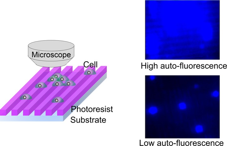
However, one of the problems affecting the performance of the SU-8 photoresist is the auto-fluorescence that occurs during the fluorescence microscopy observation of bio-samples. Both the photo-initiator and the epoxy resin in the SU-8 photoresist contain benzene rings, which exhibit considerable auto-fluorescence.20 In bio-application, fluorescent-stained bio-samples are observed using a fluorescence microscope, as shown in Fig. 1. The background noise from the substrate auto-fluorescence and that of the microstructures under the bio-samples reduces the accuracy of the observation. In an attempt to overcome this problem, Pai et al.21 have examined the low-fluorescence thick 1002 F photoresist for bio-application. The 1002 F photoresist is more suitable for fluorescence observation than the SU-8 photoresist. However, the processing specifications of the 1002 F photoresist, which yield a minimum dimension of 5 μm and a maximum aspect ratio of 4, are inferior to a minimum dimension of 1–2 μm and aspect ratio of over 10 of the SU-8 photoresist.22,23 As an alternative, the SJI photoresist, a novel thick photoresist produced by Daicel Corp. and proposed and evaluated here, has low auto-fluorescence that renders it suitable for bio-application.
FIG. 1.
Schematic of fluorescence microscope observation of bio-samples on microstructures exhibiting auto-fluorescence. Biological samples such as cells and DNA are often observed using fluorescence microscopy with a CCD camera. If cells are observed on a photoresist having high auto-fluorescence, quantitative analysis becomes difficult. This is because it is difficult to differentiate between the target samples and photoresist as a result of the low contrast ratio (S/N ratio), and because the lighting exceeds the dynamic range of the CCD camera. So, microstructures composed of low-auto-fluorescence photoresist are required for the generation of high-contrast images. Upper fluorescence image is shown as an example of cells image with high auto-fluorescence of SU-8 micropatterns, and lower fluorescence image as an example of cells with low auto-fluorescence of SJI micropatterns.
This paper proposes and evaluates the novel low-auto-fluorescence SJI photoresist. We evaluate spin coating thickness controllability and patterning errors in the exposure process as a means of determining the processing accuracy of the SJI photoresist. Then, we measure the maximum aspect ratio by fabricating microstructures composed of SJI photoresist. Finally, we demonstrate a chromosome extension device composed of SJI photoresist in order to confirm the validity of fluorescence microscope observation using this photoresist.
II. EXPERIMENTAL METHOD
A. Materials
To reduce the auto-fluorescence of the SJI photoresist, a cyclohexane ring is substituted in place of the benzene ring used in the SU-8 photoresist. Note that this benzene ring emits fluorescence through the absorption of UV light in the photo-initiator and the epoxy resin of the SU-8 photoresist. Also, the biocompatibility of the SJI photoresist is further improved by substituting phosphorus for antimony, which has cytotoxicity. The SJI photoresist is created by mixing 4 vol. % photo-initiator and 96 vol. % epoxy resin with viscosity ranging from 50–18 000 mPa·s, using a planetary stirring machine (Mazerustar, Kurabo Co.). The polymerization of the resin is achieved by generating a strong acid through the decomposition of the photo-initiator in the SJI photoresist under UV exposure.
B. Sample preparation for processing evaluation
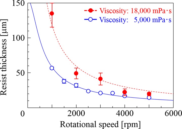
Similar to a conventional thick photoresist, the SJI photoresist is coated using the spin coating method after hexamethyldisilazane (HMDS) treatment to achieve adhesion between the substrate and photoresist. Then, the coated photoresist is soft-baked at 95 °C for 30 min to volatilize the solvent. Figure 2 shows the relationship between the coated resist thickness, t, and the rotational speed used in the spin coating process. The value of t is calculated from24
| (1) |
where v is the rotational speed and μ is the viscosity. The symbols a and b are arbitrary constant obtained by optimizing from the measured thickness of coated photoresist. The solid and dashed lines in Fig. 2 are fitting curves calculated using Eq. (1), for SJI photoresists with 5000 and 18 000 mPa·s viscosity, respectively. The lines are calculated by Eq. (1) with a = 149, and b = 0.03. From the figure, the coated film thickness is in inverse proportion to the rotational speed. It can be seen that the SJI photoresists have coating thicknesses of 10–150 μm, which are typical values for thick photoresists.
FIG. 2.
Resist thickness as a function of rotational speed in spin coating. In general, the resist thickness increases with the resist viscosity in the spin coating method; however, a high-viscosity resist can have a swollen surface coating, and a large reproducibility error exists.
The coated SJI photoresist on the substrate is subjected to 1000–4000-mJ/cm2 exposure at 365-nm wavelength using an exposure unit (ML-501D/B, Ushio Inc.) with a ± 5 nm band-pass filter through a photo mask with L-shaped lines and gaps. Then, the exposed SJI photoresist is post-exposure baked at 95 °C for 5 min in order to activate the polymerization reaction. After cooling to room temperature, the SJI photoresist is developed with propylene glycol monomethyl ether acetate (PGMEA), rinsed with 2-propanol, and dried with nitrogen.
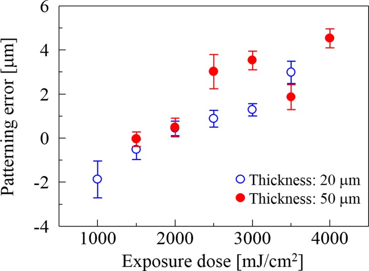
The fabricated structures made of the SJI photoresist are observed from the side using a scanning electron microscope (SEM). The patterning error is defined as the difference between the specific patterns on the photomask and those of the fabricated structures. Figure 3 shows the relationship between the exposure dose and the patterning error as obtained from the SEM images. The patterning error is correlated with the exposure dose in the 1000–4000-mJ/cm2 range, because diffusion of the acid in the photoresist actively occurs with increased exposure dose. In the case of the photoresist with a coating thickness of 50 μm and exposure dose of 1000 mJ/cm2, the microstructure is peeled from the substrate during the development process, because the exposure dose yields insufficient adhesion strength between the photoresist and the substrate. Therefore, thick-coated photoresists require higher exposure doses than thin-coated devices.
FIG. 3.
Patterning error as a function of exposure dose. The patterning error is evaluated based on a cross-sectional view of the micropatterns observed using SEM. Since a large amount of acid is generated by the photo-initiator, which propagates the cross-link reaction widely, the patterning error is proportional to the exposure dose.
C. Fluorescence emission spectra
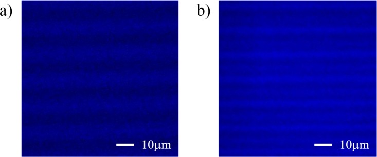
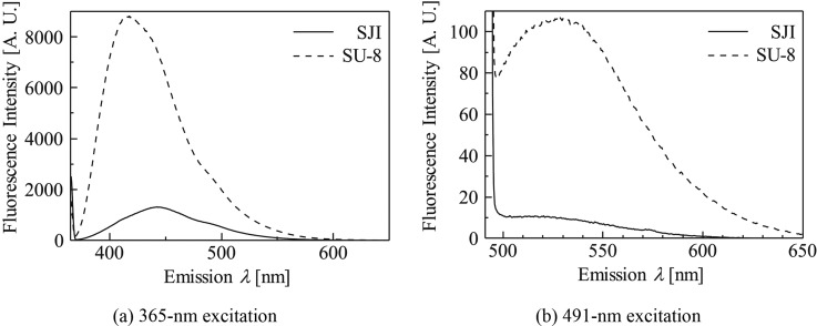
The fluorescence emission spectra of the photoresists were measured using a fluorescence spectrophotometer (F-2500, Hitachi High-Tech Corp.) and a small fluorimeter glass cell filled with the photoresist. The fluorescence intensities of the sample at emission wavelengths of 365–650 nm (using a ±5-nm band-pass) were obtained for wavelength excitations of 365 nm and 491 nm; these conditions are identical to the commonly used nuclear and chromosome counterstain DAPI (excitation/emission wavelength: 365/461 nm) and the nucleic acid YO-PRO-1 (Life Technologies Corp., excitation/emission wavelength: 491/509 nm) observation conditions. YO-PRO-1 is the conventional fluorescence labeling reagent used in DNA analysis. All fluorescence images in this paper are taken by an optical sectioning microscopy with a charge-coupled device (CCD) camera (COOLSNAPHQ2, CORNES Technologies) and an objective lens (60× oil 1.42 NA). Figure 4 shows fluorescence images of top view of the fabricated SJI and SU-8 micropatterns under same imaging parameters.
FIG. 4.
Fluorescence images of the fabricated SJI and SU-8 micropatterns without a biological sample (Filter cube: DAPI, Exposure time: 0.5 sec, and ND filter: 100%). (a) Top view of SJI micropattern (Fluorescence intensity: Min = 189, Max = 373). (b) Top view of SU-8micropatterns (Fluorescence intensity: Min = 2529, Max = 3437).
III. RESULTS AND DISCUSSION
A. Processing evaluation
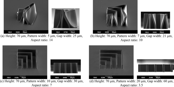
Microstructures with pattern widths of 5–20 μm were fabricated using SJI photoresists with coated thicknesses of 70 μm on glass substrate. Figure 5 shows SEM images of the fabricated microstructures. It is apparent that, for pattern widths of 5 and 7 μm, the high-aspect-ratio microstructures are distorted by surface tension during the drying process and by a lack of adhesive strength. On the other hand, for pattern widths of 10 and 20 μm, the microstructures with aspect ratios of over 7 are accurately fabricated. However, micropattern sticking is observed for samples with narrow gap widths, which is due to the large surface tension. This occurs even if the microstructures have pattern widths of 10 and 20 μm. Moreover, in cases involving coated thickness values of less than 5 μm, microstructures with pattern widths of 1.5 and 3 μm are fabricated as shown in Fig. 6. Low-aspect-ratio microstructures are easy to construct, because there is sufficient low adhesive strength between the photoresist and the substrate. These results suggest that the SJI photoresist has wide processing properties for a microstructure with an aspect ratio of over 7, in the case of a thick film, or a highly fine pattern width of 1.5 μm, in the case of a thin film.
FIG. 5.
SEM images of microstructures for 1500-mJ/cm2 exposure. The fabricated structures with aspect ratios of over 10 are distorted and collapsed as a result of sticking phenomena due to the surface tension force after the isopropyl alcohol (IPA) rinse. On the other hand, the structures with aspect ratios of less than 7 are stably fabricated.
FIG. 6.

SEM images of microstructures with 1000-mJ/cm2 exposure. For microstructures with 5-μm height (b), the minimum pattern width of 3 μm is fabricated on a glass substrate.
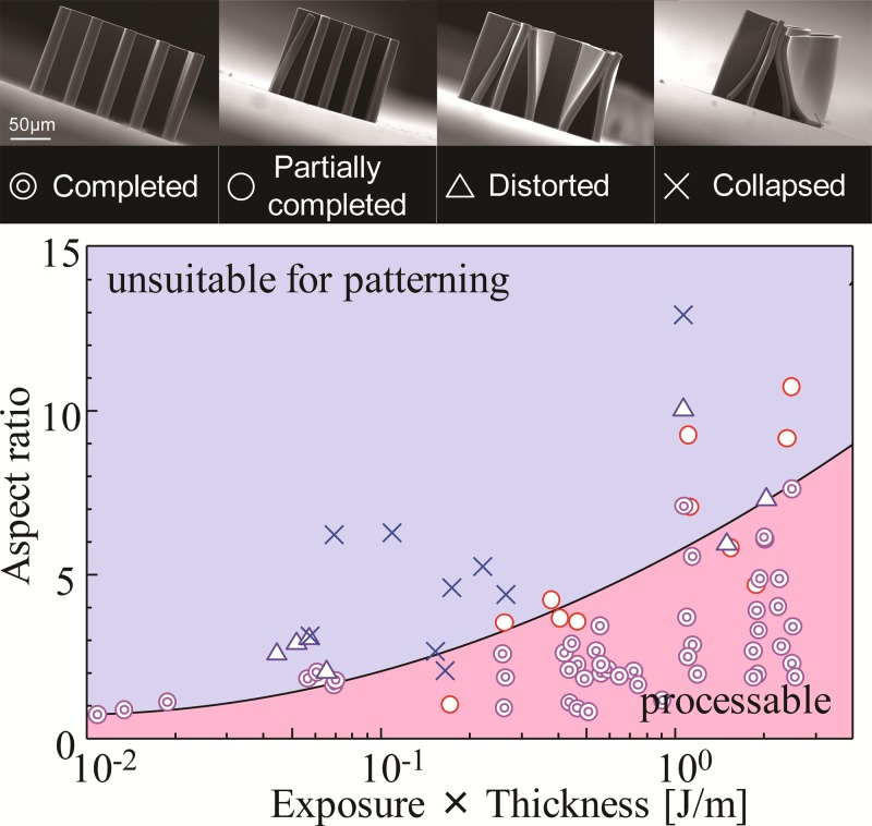
The relationship between the aspect ratio and the fabricated states of the microstructures was evaluated, and the results are shown in Fig. 7. The vertical axis is the aspect ratio of the fabricated microstructures, while the horizontal axis shows the product of the exposure dose and the resist thickness. The fabricated states are divided into 4 types, i.e., completed, partially completed, distorted, and collapsed structures, based on the cross-sectional-view SEM images. The processable conditions begin at the lower right corner of the figure, and the high-aspect-ratio microstructures are fabricated in proportion to the exposure dose and the resist thickness. The adhesive force and area between the photoresist and the substrate increase with the exposure dose and resist thickness according to a constant aspect ratio, respectively. So, the appropriate conditions for SJI photoresist patterning are determined by the dimensions of the designed structure.
FIG. 7.
Processable conditions for high-aspect-ratio microstructures. The double and single circles indicate that a completed or a partially completed structure has been fabricated under these conditions. The triangles indicate that a sticking-distorted structure has been obtained, while the crosses represent patterning structure collapses and/or flaking from the substrate. The solid line is an approximated curve that is obtained from the partially completed and distorted points, and represents the boundary between the processable and unsuitable conditions.
B. Fluorescence emission spectra
Figure 8 shows fluorescence emission spectra up to 650-nm emission under excitation wavelength of 365 nm and 491 nm. The emission spectra intensities of the SJI photoresist are reduced overall compared to those of the SU-8 photoresist. At approximately 461 nm, which is the emission wavelength of the commonly used nuclear and chromosome counterstain, DAPI (excitation: 365 nm), the fluorescence intensity of the SJI photoresist is 80% less than that of the SU-8 photoresist. At approximately 509 nm, which is the emission wavelength of the nucleic acid, YO-PRO-1 (excitation: 491 nm), the fluorescence intensity of the SJI photoresist is 90% less than that of the SU-8 photoresist. Since the SJI photoresist has a cyclohexane ring in place of the benzene ring in the SU-8 photoresist, UV absorption is prevented because the pi-electron of the benzene ring is not present.
FIG. 8.
Fluorescence emission spectra. The dashed and solid lines are the fluorescence emission spectra of the SU-8 and SJI photoresists, respectively.
IV. BIO-APPLICATION
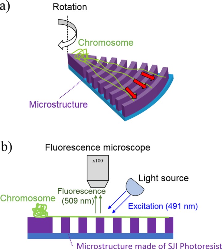
To confirm the validity of the SJI photoresist for use in fluorescence observation in bio-applications, we have demonstrated the fluorescence analysis of chromosome fibers using a chromosome extension device25 composed of SJI photoresist. Figure 8 shows the schematics of the chromosome fiber preparation technique, which is performed on a disk-like device. A centrifugal force is then applied to the device, which is a principle applied to all operations; this stretches the human chromosomes for fluorescence in situ hybridization (FISH) analysis. The device has concentric-circular micro walls (height/width: 5/5 μm) on the glass substrate, as shown in Fig. 9. Since the micro walls function as a bridge pier for chromosome suspension bridges, FISH analysis on the chip is 5 times faster than the conventional method.25
FIG. 9.
Schematics of chromosome fiber preparation technique on a disk-like device. (a) Chromosome extension by centrifugal force. The photoresist device has concentric micro wall structures that suspend the chromosomes in the fluid. The chromosomes are simply extended by the centrifugal force that is generated when the device is rotated. (b) Observation of chromosomes extended on photoresist microstructures. The suspended chromosomes on the microstructures are fluorescently observed using YO-PRO-1 staining (excitation/emission wavelengths: 491/509 nm).
To perform the chromosome extension, cells are first dropped on the center of device. Next, chromosomes are extracted using cell lysis treatment and suspended on the micro walls after extension by the centrifugal force. Then, the suspended chromosome fibers are stained using YO-PRO-1.
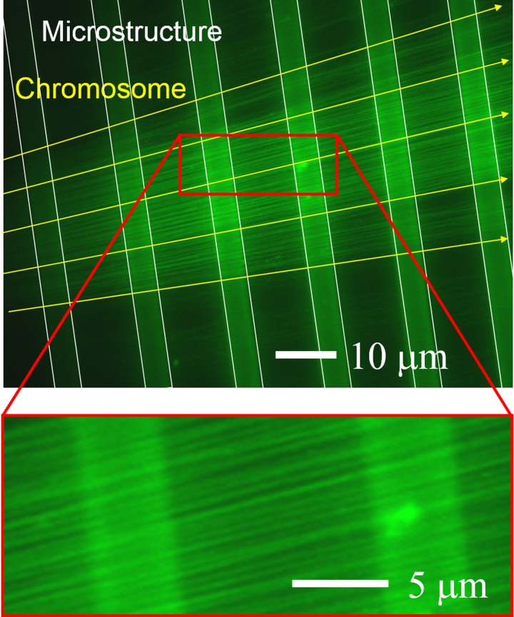
Fluorescence images of the chromosome fibers observed on the photoresist micro walls are shown in Fig. 10. The white lines indicate the outlines of the micro walls, while the yellow lines show the direction in which the chromosome fibers suspended on the microstructures were stretched. From the fluorescence images, it can be confirmed that the suspended chromosome fibers on the micro walls made of SJI photoresist are visible using fluorescence microscopy. So, the auto-fluorescence of the SJI photoresist is sufficiently low to allow chromosome fibers with low fluorescence intensity to be observed.
FIG. 10.
Fluorescence image of chromosomes extended on SJI photoresist microstructures. The fiber chromosomes are suspended on microstructures and extended in the radial direction. They are clearly observed with high contrast.
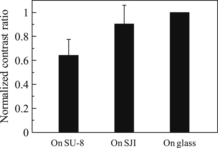
To evaluate the quantitative fluorescence observability, we compared chromosome extension devices made of SJI and SU-8 photoresist. The contrast ratio (S/N ratio) was obtained from the fluorescence images of the chromosome extension using image analysis. The fluorescence intensity was plotted for three backgrounds, i.e., the SJI photoresist, the SU-8 photoresist, and a glass substrate, along a vertical measurement line (with respect to the chromosome stretching direction), as shown in Fig. 11. The contrast ratio shows the greatest difference in the fluorescence intensity along the line, and is a typical index of fluorescence observability. Figure 12 shows the normalized constant ratio on each background based on the contrast ratio of the suspended chromosome fibers on the glass substrate (with the lowest fluorescence). The normalized contrast ratio of the SJI photoresist was 50% greater than that of the SU-8 photoresist. So, it can be concluded that the low auto-fluorescence properties of the SJI photoresist yield sufficient fluorescence observability for this device to be used in bio-application. It can also be assumed that the contrast ratio of a microdevice made of SJI photoresist increases with the decrease in background noise, because the auto-fluorescence intensity of the SJI photoresist was reduced by approximately 90% at 491-nm excitation and 509-nm emission. Although it is difficult to conduct a quantitative comparison between the spectra and fluorescence images, based on the change in the fluorescence intensity along with the CCD gain, excitation intensity, and the pattern shape, the fluorescence images are obtained with high contrast. This is due to the decreased auto-fluorescence of the photoresist.
FIG. 11.

Contrast ratio measurement method. (a) Fiber chromosomes on SU-8 photoresist or glass. (b) Fiber chromosomes on SJI photoresist or glass. The solid line is the fluorescence intensity along a scanning line on the resist, and the dashed line shows the intensity along the line on glass. The fluorescence intensity along the overall scanning line on the resist is larger than the intensity on the glass, because the background noise is increased by the auto-fluorescence of the resist. So, the difference in fluorescence intensity of the fiber chromosome on the resist is less than that of the same chromosome on glass.
FIG. 12.
Normalized contrast ratio of fiber chromosome for SU-8 photoresist, SJI photoresist, and glass substrate. Since the normalized contrast ratio on the SJI photoresist is near that on the glass substrate, the microchip made of SJI photoresist has good fluorescence observability. The number of measurement lines used for each material was twenty.
V. CONCLUSION
In this study, we have proposed and evaluated a novel low-auto-fluorescence photoresist (the SJI photoresist) that is suitable for bio-application. To evaluate the fabrication workability, we fabricated microstructures with aspect ratios of over 7 (thick film) or with gap widths of 1.5 μm (thin film). Furthermore, we fabricated a chromosome extension device composed of the proposed photoresist and demonstrated fluorescence microscope observation of chromosome fibers on the device. The experimental results indicate that the SJI photoresist has suitable observability for bio-application, along with the required patterning properties of high aspect ratio and high microstructure fineness.
ACKNOWLEDGMENTS
This work was partly supported by a Grant-in-Aid for Scientific Research (B) (Grant No. 26289067) and by the Kagawa University Nanotechnology supporting office as part of the MEXT, JAPAN “Nanotechnology Project.”
References
- 1.Terao K., Shimizu K., Miyanishi N., Shimokawa S., Suzuki T., Takao H., and Oohira F., Analyst 137, 2192 (2012). 10.1039/c2an16010b [DOI] [PubMed] [Google Scholar]
- 2.Carlo D. D., Wu L. Y., and Lee L. P., Lab Chip 6, 1445 (2006). 10.1039/b605937f [DOI] [PubMed] [Google Scholar]
- 3.Warkiani M. E., Lou C. P., and Gong H. Q., Biomicrofluidics 5, 036504 (2011). 10.1063/1.3637630 [DOI] [PMC free article] [PubMed] [Google Scholar]
- 4.Martinez E., Engel E., Planell J. A., and Samitier J., Ann. Anat. 191, 126 (2009). 10.1016/j.aanat.2008.05.006 [DOI] [PubMed] [Google Scholar]
- 5.Inoue M., Okonogi A., Terao K., Takao H., Shimokawa F., Oohira F., Kotera H., and Suzuki T., Micro Nano Lett. 7, 725 (2012). 10.1049/mnl.2012.0216 [DOI] [Google Scholar]
- 6.Yamashita H., Terao K., Takao H., Shimokawa F., Namazu T., Oohira F., and Suzuki T., in Proceedings of the IEEE Optical MEMS & Nanophotonics Conference 2013, Kanazawa, Japan, 18 August–22 August 2013 (IEEE, 2013), pp. 69–70. [Google Scholar]
- 7.Meier R. C., Badilita V., Brunne J., Wallrabe U., and Korvink J. G., Biomicrofluidics 5, 034111 (2011). 10.1063/1.3613668 [DOI] [PMC free article] [PubMed] [Google Scholar]
- 8.Nakahara T., Hosokawa Y., Terao K., Takao H., Shimokawa F., Oohira F., Namazu T., Kotera H., and Suzuki T., 2012 IEEE 25th International Conference on Micro Electro Mechanical Systems (MEMS), 29 January 2012–2 Februaray 2012 (IEEE, 2012), pp. 1181–1184 10.1109/MEMSYS.2012.6170374 [DOI] [Google Scholar]
- 9.Suzuki T., Yamamoto H., Ohoka M., Kanno I., Washizu M., and Kotera H., Miniaturized Systems for Chemistry and Life Science (MicroTAS2007): Proceedings of the 11th International Conference on Miniaturized Systems for Chemistry and Life Science, Paris, France, 7 August–11 August 2007 (Royal Society of Chemistry, 2007), pp. 1765–1767. [Google Scholar]
- 10.Xu Y., Xie F., Qiu T., Xie L., Xing W., and Cheng J., Biomicrofluidics 6, 016504 (2012). 10.1063/1.3687399 [DOI] [PMC free article] [PubMed] [Google Scholar]
- 11.Sato H., Yagyu D., Ito S., and Shoji S., Sens. Actuators A 128, 183 (2006). 10.1016/j.sna.2005.12.043 [DOI] [Google Scholar]
- 12.Zhang Z., Zhao P., Xiao G., Watts B. R., and Xu C., Biomicrofluidics 5, 046503 (2011). 10.1063/1.3659016 [DOI] [PMC free article] [PubMed] [Google Scholar]
- 13.Yang R. and Wang W., Sens. Actuators B 110, 279 (2005). 10.1016/j.snb.2005.02.006 [DOI] [Google Scholar]
- 14.Auzelyte V., Elfman M., Kristiansson P., Nilsson C., Pallon J., Marrero N. A., and Wegdén M., Microelectron. Eng. 83, 2015 (2006). 10.1016/j.mee.2006.04.001 [DOI] [Google Scholar]
- 15.Liu G., Tian Y., and Kan Y., Microsyst. Technol. 11, 343 (2005). 10.1007/s00542-004-0452-x [DOI] [Google Scholar]
- 16.Morikaku T., Kaibara Y., Inoue M., Miura T., Suzuki T., Oohira F., Inoue S., and Namazu T., J. Micromech. Microeng. 23, 105016 (2013). 10.1088/0960-1317/23/10/105016 [DOI] [Google Scholar]
- 17.Sato H., Kakinuma T., Go J. S., and Shoji S., Sens. Actuators A 111, 87 (2004). 10.1016/j.sna.2003.10.009 [DOI] [Google Scholar]
- 18.Yang B., Dukkipati V. R., Li D., Cardozo B. L., and Pang S. W., J. Vac. Sci. Technol. B. 25, 2352 (2007). 10.1116/1.2806975 [DOI] [Google Scholar]
- 19.Esch M. B., Sung J. H., Yang J., Yu C., Yu J., March J. C., and Shuler M. L., Biomed. Microdev. 14, 895 (2012). 10.1007/s10544-012-9669-0 [DOI] [PubMed] [Google Scholar]
- 20.Walczak R., Sniadek P., and Dzuyban J. A., Optica Applicata 41, 873 (2011). [Google Scholar]
- 21.Pai J., Wang Y., Salazar G., Slms C., Bachman M., Li G. P., and Allbrltton N., Anal. Chem. 79, 8774 (2007). 10.1021/ac071528q [DOI] [PMC free article] [PubMed] [Google Scholar]
- 22.Lorenz H., Despont M., Fahrni N., LaBianca N., Renaud P., and Vettiger P., J. Micromech. Microeng. 7, 121 (1997). 10.1088/0960-1317/7/3/010 [DOI] [Google Scholar]
- 23.Anhoj T. A., Jorgensen A. M., Zauner D. A., and Hübner J., J. Micromech. Microeng. 16, 1819 (2006). 10.1088/0960-1317/16/9/009 [DOI] [Google Scholar]
- 24.Levinson H. J., Principles of Lithography, 2nd ed. ( SPIE Press, Bllingham, 2005), p. 63. [Google Scholar]
- 25.Suzuki T., Terao K., Suzuki H., Nitta Y., Takao H., Shimokawa F., Hiramaru D., and Kotera H., in Miniaturized Systems for Chemistry and Life Sciences (MicroTAS2012): The 16th International Conference on Miniaturized Systems for Chemistry and Life Sciences, Okinawa, Japan, 28 October–2 November 2012 (Royal Society of Chemistry, 2012), pp. 272–274. [Google Scholar]


