

Abstract
We have previously reported on dMiCE, a method of resolving depth or interaction (DOI) in a pair of discrete crystals by encoding light sharing properties as a function of depth in the interface of a crystal-element pair. A challenge for this method is the cost and repeatability of interface treatment for each crystal pair. In this work, we report our preliminary results on using sub-surface laser engraving (SSLE) as a means of forming this depth-dependent interface in a dMiCE detector. A surplus first-generation SSLE system was used to create a partially reflective layer 100-microns thick at the boundary between two halves of a 1.4-by-2.9-by-20 mm3 LYSO crystal. The boundary of these paired crystal elements was positioned between two 3-mm wide Silicon photomultiplier arrays. The responses of these two photodetectors were acquired for an ensemble of 511-keV photons collimated to interact at a fixed depth in just one crystal element. Interaction position was then varied to measure detector response as a function of depth, which was then used to maximum-likelihood positions. Despite use of sub-optimal SSLE processing we found an average DOI resolution of 3.4 mm for front-sided readout and 3.9 mm for back-sided readout while obtaining energy resolutions on the order of 10%. We expect DOI resolution can be improved significantly by optimizing the SSLE process and pattern.
Index Terms: Depth of interaction, laser etching, nuclear medicine detectors, PET detectors, radiation detectors, scintillators
I. Introduction
dMiCE is a discrete scintillation detector design that uses depth-dependent light sharing between a pair of crystals to encode depth-of-interaction (DOI) information in the light readout from one end of this crystal pair. Previous work [1] to select a conventional surface treatment (Fig. 1) that would optimize depth resolution for a pair of 2-by-2-by-20 mm3 crystals resulted in the use of multiple layers of shaped mirror film reflectors (VM2000 by 3M) and a coating of high-index optical adhesive (Meltmount-1.705 by Cargille Labs) sandwiched between a pair of partially roughened crystals. The non-shared crystal surfaces are wrapped in Teflon. The crystal surface in the optically coupled region was roughened with 600-grit sandpaper. The measured detector response as a function of interaction depth shows excellent depth sensitivity. However, fabrication of this crystal pair was laborious and difficult to repeat without a refined fabrication process. Furthermore, the non-scintillating interface material reduced overall photodetection efficiency.
Fig. 1.
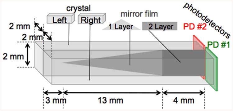
Conventional dMiCE design rported in prior work with two layers of mirror film (one triangular, one square) between the crystals [1].
In this work, we examine the use of sub-surface laser engraving (SSLE) to control light distribution without having to cut and manually form an interface. SSLE is a fast and relatively inexpensive process that has been used to produce 3D art in crystal blocks and recently has been used to discretize scintillation crystals [2], [3]. A pulsed focused laser is used to create a pattern of microscopic optical defects that can reflect and scatter light. We have proposed to use SSLE as a means of shaping the light response function in scintillation detectors. Specifically, in this work, we examine depth and energy resolution of dMiCE crystals created using a SSLE interface. We compare these results to that of a dMiCE crystal with a mechanically fabricated interface comprised of shaped mirror film and optical adhesive [1].
II. Materials and Methods
We fabricated several dMiCE crystals using sub-surface laser engraving. Before and after engraving, we measure photopeak detector response statistics of these samples to 511-keV gamma rays as a function of depth. An independent set of photopeak events at each depth were then positioned by maximum-like estimation. Depth resolution of these detector samples is reported as a function of depth.
We initially sought to use a commercial engraving service or to develop collaboration with a commercial company interested in application of SSLE to scintillators. Those efforts were not successful due to a combination of inadequate accuracy from the several engraving services we sent samples to and excessive demands/costs from potential commercial collaborators.
As a practical alternative, we have made use of a surplus first-generation SSLE system (Fig. 2) by Crystalix Evolution GmbH, Germany, to conduct a proof-of-concept study of SSLE used to form a light-sharing interface. Although we refurbished the controller, this 13-year-old system suffers from optical aberrations in the flat-field lens and an unstable Q-switching. These issues caused the engraved interface to be inconsistent and non-uniform (e.g. Fig. 3), which prevents us from conducting an optimization of the interface pattern. However, this system is sufficient to as a proof-of-concept that will motivate future work with a next-generation SSLE system (see Discussion and Fig. 31).
Fig. 2.
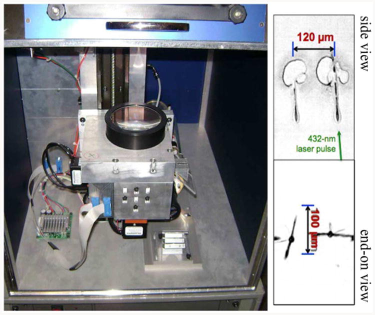
Left is shown the surplus first-generation sub-surface laser engraving system by Crystalix Evolution GmbH used for this work. A confocal microscope image of point defects produced with this system exhibit significant collateral damage, as shown to the right.
Fig. 3.
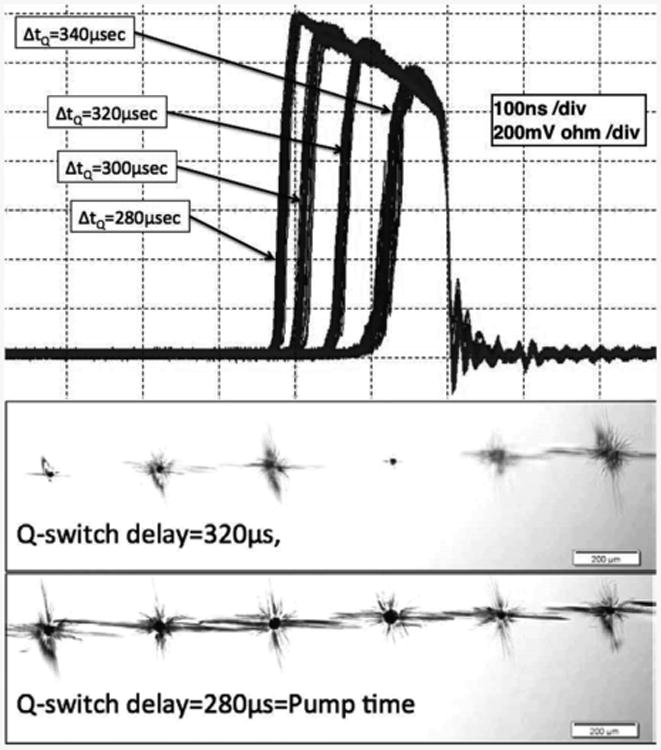
(top) laser pulse profile for several Q-switching delays measured with a PiN diode and a 1-Mohm load on a 1 GHz Tektronix Oscilloscorpe. (bottom) a line of SSLE defects produced for two Q-switching delays.
Fig. 31.
Left is shown our next generation sub-surface laser engraving system by Crystalix Evolution GmbH. A confocal microscope image of point defects produced by this system using optimized laser-pulse profile is at the right.
A. Engraving
The surplus SSLE system we used for this study has a 200-Hz pulsed Nd-YAG laser (1064 nm) with peak power of 15 kW and adjustable pulse duration (80 to 210 nsec). The laser is steered by a pair of IR-mirrors on controlled galvanometers and is focused to a controlled depth using a 80-mm-focallength telecentric flat-field lens mounted on a vertical linear stage.
Our only control of the pulse profile was through the Q-switching delay, which determined how long after the laser cavity energy-pump is started that the pulse is released. The cavity is pumped until saturated (280 μsec). The top of Fig. 3 shows the laser pulse profile for several Q-switching delays. The bottom of Fig. 3 shows a series of SSLE defects produced in LYSO for two of these pulse profiles. Above 320 – μsec Q-switching delay, the defect size varied significantly (sometimes not appearing). However, the defect size grew significantly for smaller Q-switching delay. Therefore, for the remainder of this work, we used the smallest possible pulse width that consistently produced defects at every position (a Q-switching delay of 300 μsec and pulse width of 180-nsec). The resultant size of defects is about 100 microns.
We engraved 1.4 × 2.9 × 20 – mm3 LYSO crystals, producing an interface down the middle as shown in Fig. 4. Either one or two layers of optical defects (patterns shown in Fig. 4) were used to examine if we could affect the amount of light shared between these crystal halves. The second layer of points in the 2-layer pattern were offset from the first layer to improve reflectivity and to allow these layers to be brought as close together as possible with our surplus SSLE system.
Fig. 4.
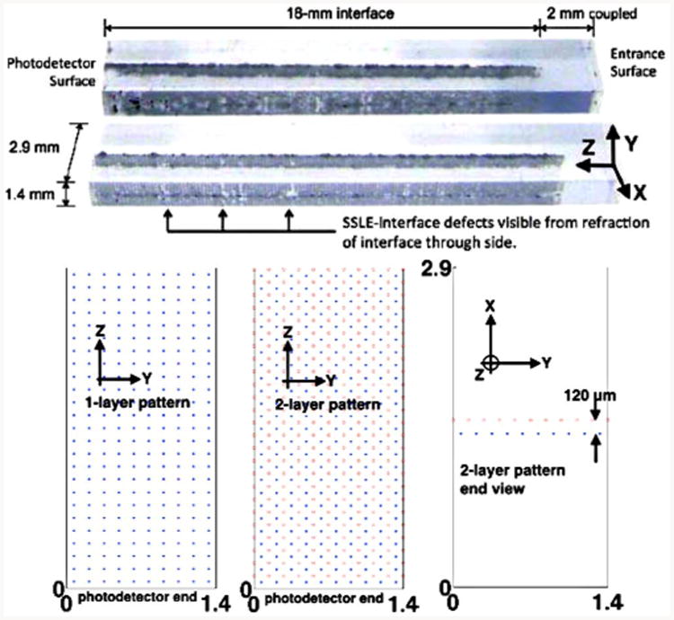
(top) Two SSLE dMiCE crystals engraved by the system in Fig. 2; their interfaces are one layer of SSLE points on a 120 μm-grid spacing. (bottom) One-layer and two-layer SSLE interface patterns; patterns extend in the z-direction over 18 mm from the photodetector surface.
B. Detectors
We calibrated and evaluated seven 20-mm-tall dMiCE crystals (Table I). We also examined the responses of crystals 1a, 1b, and 1c before SSLE. Due to crystal availability, sizes of the two mechanically coupled crystal pairs (MFa and MFb) are different from the SSLE crystal pairs.
Table I. Description of Tested dMiCE Crystal Samples.
| Sample ID | L×W [mm] | Interface Description | SSLE step [μm] |
|---|---|---|---|
| La | 1.4×2.9 | 1 SSLE layer (see Figure 4) | 140 |
| Lb | 1.4×2.9 | 1 SSLE layer (see Figure 4) | 140 |
| Lc | 1.4×2.9 | 1 SSLE layer | 120 |
| 2a | 1.4×2.9 | 2 SSLE layers (160 μm apart) | 120 |
| 2b | 1.4×2.9 | 2 SSLE layers (160μm apart) | 120 |
|
|
|||
| MFa | Two 1.4×2.9 | BC630 grease, 18mmVM2000 on 1.4×20 mm2 side | n/a |
|
|
|||
| MFb | Two 2.0×2.0 | Meltmount & 18mm VM2000 on 2×20 mm2 side (Figure 1) | n/a |
Two photodetectors (PD1 and PD2) are used in a 15.0°C ± 0.2°C temperature regulated dark box to read out the partitioned end of a dMiCE crystal. Our final detector configuration will consist of a 1-to-1 coupling of crystal halves (1.4 × 1.45mm2 area) to a monolithic SiPM array from AvidSid (Fig. 5(a)). Other than sample MFb, for the testing done in this work, we used two pixels of a 16-channel Hamamatsu C11206-0404FB MPPC photodetector array (Fig. 5(b)). All other faces of the crystals were covered in 4 layers of Teflon tape. For sample MFb, we used a 2-pixel MAPD-3N device from Zecotek Photonics Inc. operated at ambient room temperature (20.0°C ± 0.5°C)
Fig. 5.
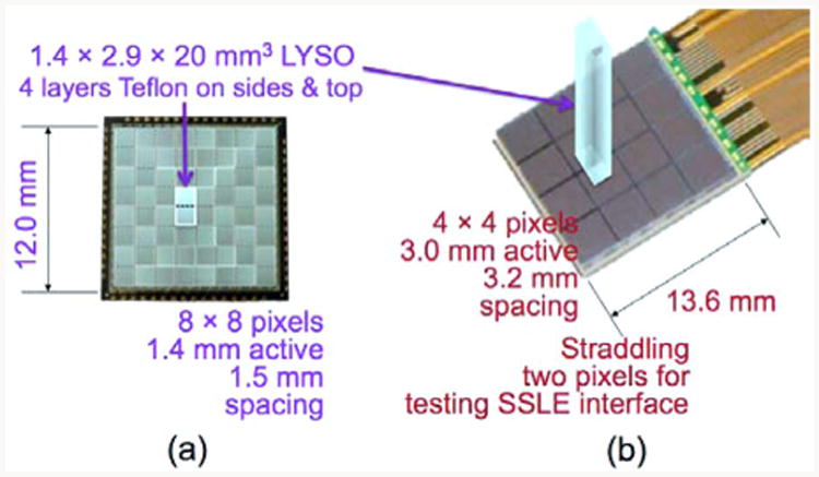
(a) AvidSid SpIM array planned for reading out 32 dMiCE crystal pairs; (b) The Hamamatsu MPPC array used for initial testing of dMiCE performance are 3-by- 3 mm2 active area.
The inactive gap between photodetectors is aligned with the interface such that scintillation light must either penetrate the interface or go all the way around the top of the interface (opposite the photodetectors) to reach the abutted photodetector. For clarity, we term the crystal over PD1 as the Left crystal, and the crystal over PD2 as the Right crystal.
C. Calibration
As described later in Section II-E, we identify the crystal of interaction and depth of interaction by maximum-likelihood estimation using a multivariate normal-probability model. For this purpose, we use a collimated 511-keV beam to calibrate the mean and variance of detector response due to photopeak events as a function of depth and crystal of interaction. In all cases, the zero energy ADC channel was determined and the system linearity checked.
For all except sample MFb, a double-ended 0.5-mm-borehole Tungsten collimator was used to collimate a Na-22 point source to produce a collimated 511-keV gamma-ray beam (Fig 7). A 4-by-4-by-20 mm3 LYSO coincidence detector read out by a Hamamatsu R9880U-110 photomultiplier tube was placed at the exit of the backend borehole in order to reduce the photon flux triggering the acquisition electronics. Moving this coincidence detector further back does not significantly improve beam size, which is primarily due to the geometry of this double-ended borehole. The collimated beam size was measured to be 0.6-mm diameter by measuring coincidence count rate as we scanned off the edge of a 0.8-mm-thick LYSO scintillator.
Fig. 7.
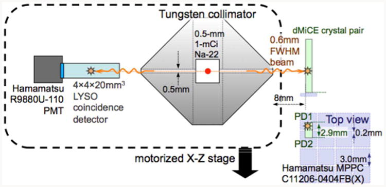
Diagram of calibration setup for the SSLE processed crystals.
The calibration beam setup for MFb (data collected as part of our earlier dMiCE detector work) did not use a bore hole collimator, but instead placed the 4-by-4-by-20 mm3 LYSO coincidence detector a distance 10 cm away, resulting in a beam size of 1.5 mm.
The collimated 511-keV gamma-ray beam was aimed at one crystal element (Left or Right) and the responses of the two photodetectors (PD1 and PD2) were read out for 5,000 to 10,000 events (Fig 7). Except for MFb, charge-integrated signals were acquired with a VME system triggered by NIM electronics (Fig 8). For the MFb sample, signals were acquired with an Ortec AD811 ADC (triggering remained the same). These measurements were repeated at each depth (step sizes indicated in Figs 12–19) for each of the dMiCE test crystals in Table I. For crystals 1c, 2a, 2b, and MFb, this process was repeated for both Left and Right crystals of the dMiCE pair. For 1a, 1b, and MFa, this process was only done for the Right crystal.
Fig. 8.
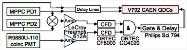
Signal acquisition setup.
Fig. 12.
Pre-SSLE detector response statistics for photopeak events in dMiCE crystals 1a, 1b, and 1c: mean (line) and ± std. deviation (error bars).
Fig. 19.
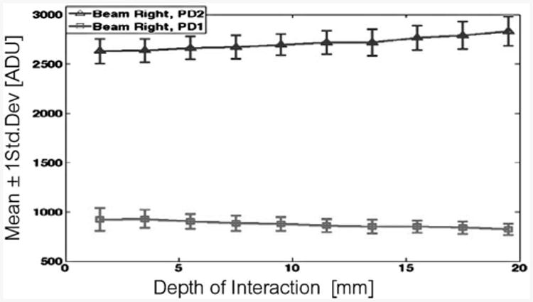
Sample MFb (mirror film and Meltmount) detector response statistics for photopeak events: mean (line) and ± std. deviation (error bars). As noted previously, the acquisition electronics for MFb were different than the rest of the crystals examined.
We do not estimate lateral position within a crystal. However, we aim to characterize the effect of lateral interaction position on the depth estimate. To examine sensitivity to lateral beam position (distance from interface), we measured mean detector response at twelve lateral beam positions separated by 0.2-mm at each of four interaction depths (3, 7, 11, and 15 mm DOI). Since the calibration beam is wider (0.6 mm) than our lateral-step size, we expect our measured response versus lateral interaction position to be smoothed. However, since we are able to distinguish interaction on either side of the interface by the classification and filtration procedure described in Section II-D, the measured response versus lateral position is not smoothed across the interface. Since we do not have exact knowledge of the beam profile, we are not able to decompose the detector response function on a 0.2-mm step size. Therefore, our measurements only resolve the response averaged over 0.4 mm at beam positions that are 0.1 mm from the interface and averaged over 0.6 mm at beam positions further away from the interface. This affords at least two distinct lateral points for this sensitivity study. Although we may consider using a finer beam for lateral sensitivity studies in future work, we were not able to allocate the added calibration time that would be required for the current study.
D. Filtering
We use only photopeak events for calibration and evaluation. For calibration of detector response statistics, photopeak events are identified in three steps (Fig. 9). First, to reject some inter-crystal scatter, we keep only events where the gain-corrected signal of the targeted crystal is more than its neighbor's. Second, to eliminate Compton escape events and 1274-keV down scatter, we consider only events within a ±17% energy window about the photopeak of the gain-corrected sum signal for PD1 and PD2. As a finally step in rejecting scatter, we only keep events within a 10% contour about the peak count-density of the joint signal distribution for PD1 and PD2 (i.e. the full-width at tenth-max contour).
Fig. 9.
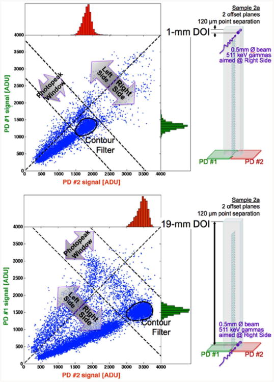
Example of event filtering for two beam positions (top) 1-mm DOI, and (bottom) 19-mm DOI. We show the beam position (left) and bivariate signal distribution (right). Univariate signal histograms of the contour-filtered data projected to the right (PD1) and top (PD2).
To test event-positioning performance, we only use the last two steps described above. In other words, events are not filtered based on which channel has the larger signal.
E. Positioning
Photopeak events of a separate test-data set are positioned by maximum likelihood (ML) estimation [4]. For this purpose, we assume signals for PD1 and PD2 (g1,g2) for a fixed interaction position, r, and energy, E, result from an independent bivariate normal distribution,N(g1,g2|r, E). The mean and variance of the filtered calibration data (e.g., from the projected distribution in Fig 9) are computed for each beam position. To reduce uncertainty in the calibrated variance, we smooth the measured variance as a function of depth using a local quadratic fit with span 13. In cases where the calibration beam step size is greater than 1 mm, these mean and variance lookup tables are interpolated using a bi-cubic spline. Examples of the resulting maps of mean and variance versus position are shown in Figs. 10 and 11. Signal statistics are reported ADU, which are digitization units of the Analog-to-Digital converter. Note that for the case shown in Fig 11, we expect the uncertainty on the response variance of interactions on the Right side to be smaller by a factor of two since we collected four times as many events on the right side than on the left side. The smoothed and interpolated mean and variance lookup tables are then use to compute a likelihood map for each event, from which we find the event's ML position estimate:
Fig. 10.
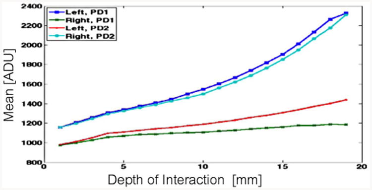
Mean response to photopeak events for both photodetectors, PD1 and PD2, of sample-2a dMiCE are reported as a function of interaction depth for when the interactions occur in the Left or Right half of this dMiCE crystal.
Fig. 11.
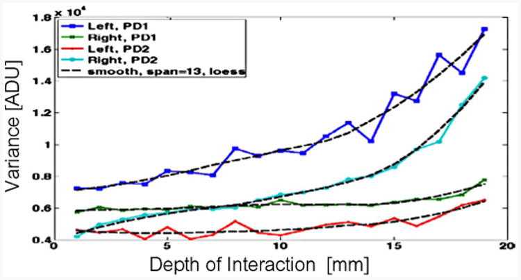
Response variance to photopeak events for both photodetectors, PD1 and PD2, of sample-2a dMiCE reported as a function of interaction depth for when interactions occur in the Left or Right half of this dMiCE crystal.
F. Resolution
The depth estimate distributions are not normally distributed. Therefore, we choose to compute depth resolution as 2.35 times the standard deviation of the ensemble distribution of event position estimates. This measure of resolution is adequate for comparing DOI-positioning performance of different dMiCE crystals. Performance of crystal identification is not fully examined in this work. However, we note that in Fig. 9, the photopeak events of the bivariate signal distribution is well separated for events interacting in the Left and Right halves of the dMiCE crystal.
We also examine energy resolution, which is computed as the ratio of the full-width at half-max of the 511-keV photopeak.
III. Results
Mean and standard deviation of detector response to photopeak events are reported versus interaction depth for the seven crystals tested in Figs. 12–19. Only the right side of the crystal was calibrated in Figs. 12–15, while both sides were examined in the remaining crystals.
Fig. 15.
Sample 1b (1-layer SSLE, 140 – μm grid) detector response statistics for photopeak events: mean (line) and ± std. deviation (error bars).
Fig. 12 shows detector response for three crystals without any interface (prior to SSLE); Due to a slight mismatch in gain and differences in solid angle of the two photodetectors we see a slight difference between the response of the two photodetectors; depth sensitivity only enters as a slight increase in total light collected for interactions closer to the photodetectors. Fig 12 also shows excellent consistency in the total and fraction of light collected by PD1 and PD2 for these three samples. This verifies consistent coupling and alignment of the crystal onto the photodetectors.
In Fig. 13, we see that manually coupling a pair of crystals with mirror film and optical grease resulted in fairly good optical isolation of the two photodetectors. However, this interface also resulted in very poor depth dependence since there was inadequate light sharing at the optically coupled end of the interface where optical grease was used. Poor optical coupling here is due to a mismatch of refractive index (1.82 for LYSO and 1.46 for the optical grease). To verify this result was not due to the narrow aspect ratio of optically coupled region, we also rotated the crystals to be coupled on a 2.9-by-20 – mm2 side. However, we observed nearly the same light coupling performance (35% versus 33% signal ratio) for interactions near the optically coupled region.
Fig. 13.
Sample MFa (mirror film and optical grease) detector response statistics for photopeak events: mean (line) and ± std. deviation (error bars).
In Fig. 19, we see that changing the coupling medium from 1.46-index optical grease to a high-index optical adhesive (Meltmount 1.705) resulted in getting significantly better depth dependence on light sharing across the interface. On the end where Meltmount was used (depth 0–4 mm), the mean responses of PD1 and PD2 are more closely matched than at the opposite end where mirror film isolates the crystals.
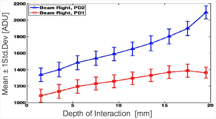
Fig. 14 and 15 also show a marked improvement in the depth dependence of light sharing across the shaped 1-layer SSLE interface. In Fig. 16, we see a further increase in this depth dependence by changing the 1-layer SSLE grid point spacing from 140 μm to120 μm.
Fig. 14.
Sample 1a (1-layer SSLE, 140 –μm grid) detector response statistics for photopeak events: mean (line) and ± std. deviation (error bars).
Fig. 16.
Sample 1c (1-layer SSLE, 120 – μm grid) detector response statistics for photopeak events: mean (line) and ± std. deviation (error bars).
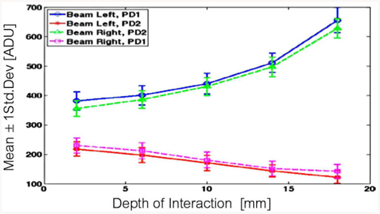
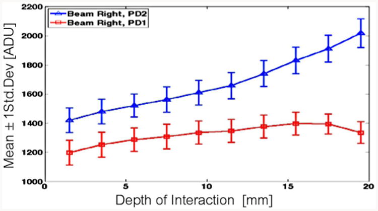
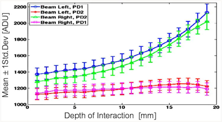
Finally, in Figs. 17 and 18 we see that 2-layer SSLE reinforces isolation of scintillation light near the photosensor; the gap in mean response of PD1 and PD2 widens near the photosensor. We note that in Fig 17 the mean response of PD2 when the beam is aimed at the left crystal differs significantly from PD1 when beam is to the right; it also differs from the response of PD2 in the equivalent configuration of Fig. 18. We thnk that in the calibration of this one crystal, there was a slight misalignment of the SSLE interface with the gap between PD1 and PD2. If the interface is offset to one side, we would expect an asymmetric light sharing by the photodetectors for interactions on the left and right sides of the interface.
Fig. 17.
Sample 2a (2-layer SSLE, 120 – μm grid) detector response statistics for photopeak events: mean (line) and ± std. deviation (error bars).
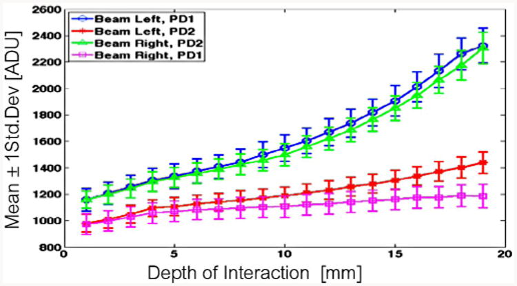
Fig. 18.
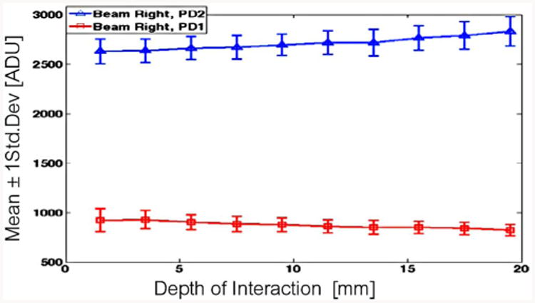
Sample 2b (2-layer SSLE, 120 – μm grid) detector response statistics for photopeak events: mean (line) and ± std. deviation (error bars).
In comparing pre-SSLE (Fig 12) and post-SSLE treatment (Figs. 14–16) of crystals 1a, 1b and 1c we observe a significant increase in light loss with depth. This may be due in part to absorption at the SSLE interface. However, if this increased light loss were due completely to absorption of light at the SSLE interface, we would expect even more light loss in the 2-layer SSLE interface. However, the light loss in the 2-layer SSLE appears similar to the 1-layer SSLE. Therefore, we think this increased light loss in all SSLE samples occurs in part to penetration of the Teflon wrapped perimeter; with the added SSLE interface, the average number of reflections of scintillation light from the Teflon (before detection) increases. This effect, which can be reproduced in optical ray-trace simulation [5], is greater when the gamma interaction is farther from the photodetectors.
Sensitivity of detector response to lateral beam position was measured at four depths (3, 7, 11, and 15-mm DOI) and is shown in Fig. 20. Crystal 2a (2-layer SSLE) was used for this purpose. As with previous results, scatter events are filtered and the crystal-of-interaction is identified using the joint distribution of signals for the two sensors. We see that the mean response is sensitive to interaction position in the upper half of the crystal, where light is more readily shared between the two photosensors.
Fig. 20.
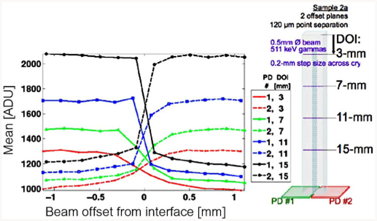
Sensitivity to lateral interaction position in sample 2a.
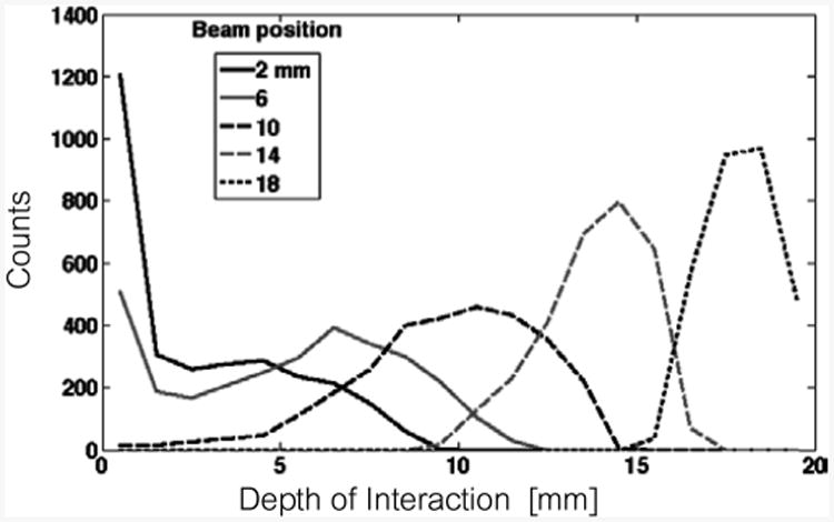
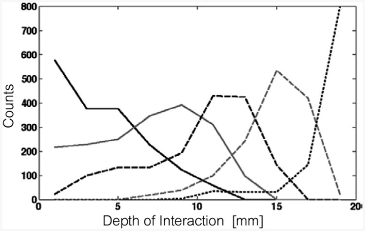
With these calibrated detector response maps, we find the ML estimate of interaction depth for an ensemble of 5,000 to 10,000 photopeak events at each depth. Estimate distributions are shown for five depths for each dMiCE sample in Figs 21–26. In each case, we find there to be a pile up of the estimates near the edge for beam positions at the end away from the photodetector (DOI < 6 – mm). This pileup is due to the relatively large signal variance compared to the change in response with depth at this end of the crystal. To facilitate comparison of the depth-positioning performance of different dMiCE crystals, we compute resolution as 2.35 times the standard deviation of the depth-estimate distribution. A summary of this resolution measure versus beam depth is given for each of the test crystals in Fig. 27. A summary of depth-prior-weighted resolution is given in Table II for front-sided and back-sided readout for each dMiCE type examined; the depth prior is taken to be an exponential with attenuation coefficient 0.83/cm from either the front or back surface.
Fig. 21.
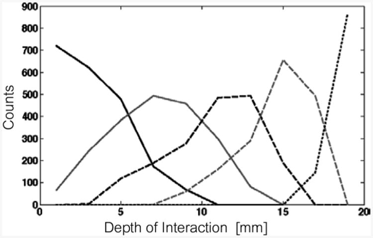
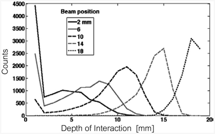
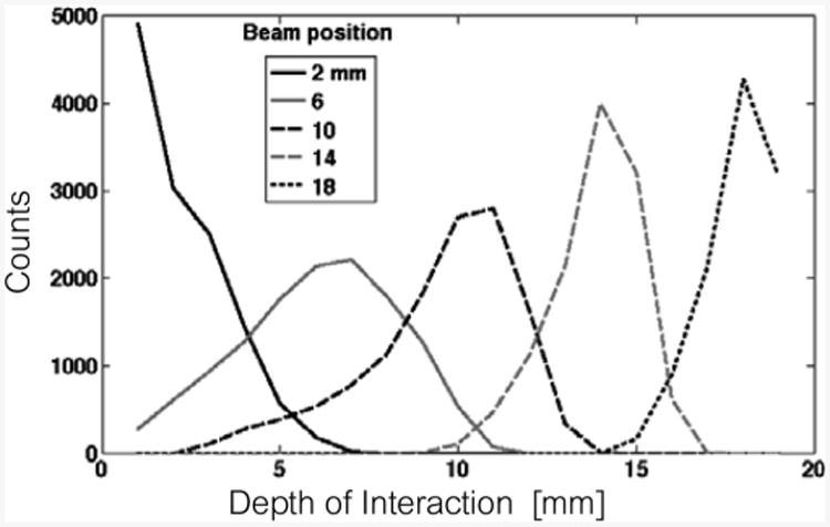
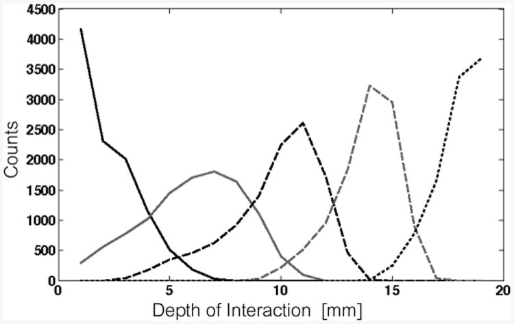
Depth-estimate distribution for five beam positions in sample 1a (1-layer SSLE, 140 – μm grid).
Fig. 26.
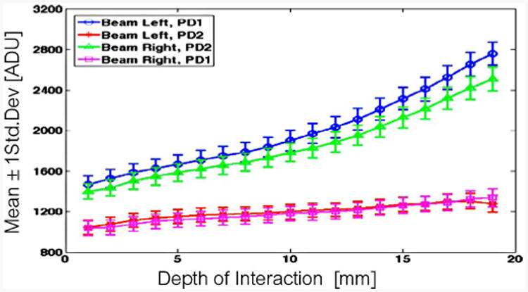
Depth-estimate distribution for five beam positions in sample MFb (mirror film and Meltmount.
Fig. 27.
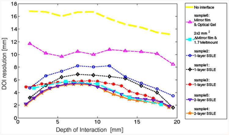
Summary of DOI position resolution versus depth of interaction for each of the dMiCE crystal treatments considered.
Table II. Summary of Depth-Prior-Weighted Resolution Versus Crystal Design.
| dMiCE interface type | Depth-prior-weighted resolution [mm] | |
|---|---|---|
| Front-sided | Back-sided readout | |
| 1-layer SSLE (avg. of la,b,c) | 4.9 | 5.6 |
| 2-layer SSLE (avg. 2a & 2b) | 3.4 | 3.9 |
| Mirror film & optical grease (MFa) | 9.9 | 10.5 |
| Mirror film & Meltmount 1.7 (MFb) | 3.6 | 4.2 |
| No interface | 15 | 16 |
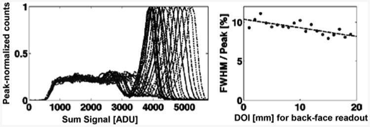
Finally, we examined energy resolution as a function of depth. We report histograms of the total signal (gain corrected sum of two photodetector channels) and energy resolution versus DOI (measured from the surface opposite the photodetectors) for a 1-layer SSLE interface (Fig. 28), a 2-layer SSLE interface (Fig. 29) and the conventional dMiCE interface (Fig. 30). Note that the horizontal scales (ADU units) are not the same in Fig. 30 compared to Figs. 28 and 29 due to the different amplifiers and acquisition electronics used for the different SiPMs utilized.
Fig. 28.
Energy histogram (left) and resolution (right) versus DOI for the 1-layer, 120-um-grid SSLE-interface dMiCE detector (Table I, sample 1c).
Fig. 29.
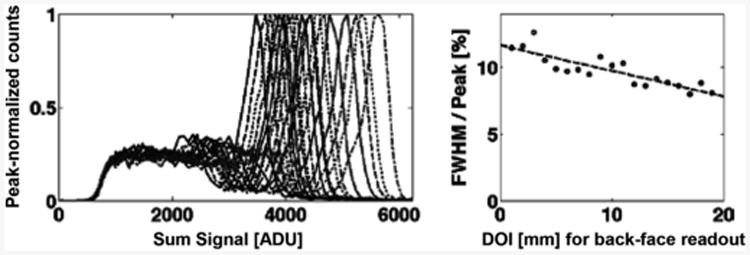
Energy histogram (left) and resolution (right) versus DOI for the 1-layer, 120-um-grid SSLE-interface dMiCE detector (Table I, sample 2b).
Fig. 30.
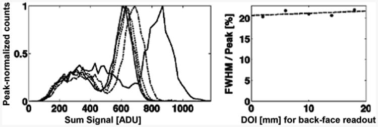
Energy histogram (left) and resolution (right) versus doi for the conventional dMiCE interface (Table I, sample MFb).
IV. Conclusion
We have shown feasibility of using Sub-Surface Laser Engraving (SSLE) to encode depth-of-interaction (DOI)information in the light-response function of a dMiCE photodetector pair. A single-layer interface of 120 – μm-spaced 100 – μm-sized SSLE microfractures resulted in a maximum-likelihood-estimate (MLE) DOI resolution between 4 mm and 8 mm over the full 20-mm depth of the dMiCE crystal. Using two such SSLE layers separated by 100 μm and with offset grid points, we obtained a MLE DOI resolution between 2 mm and 5 mm over the full depth. In both cases, DOI resolution was better near the ends closest and furthest from the photodetectors than in the region between.
Energy resolution for the 1-layer SSLE-dMiCE crystals ranged from 10.6% to 8.0%, improving at depths closer to photodetectors. Energy resolution for the 2-layer SSLE dMiCE crystals also improved at depths closer to the photodetector, ranging from 7.9% to 12.3%. Thus, improvement of optical isolation with a second SSLE layer has also increased light loss at greater distance from the photodetectors.
The energy resolution of the conventional dMiCE crystal from [1] was between 20.7% and 21.7%, nearly uniform with depth. This significant difference in energy resolution compared with the SSLE-dMiCE crystals is primarily attributed to differences in the properties (i.e. photodetection efficiency and noise characteristics) of the two Silicon photomultipliers used. With only half the signal-to-noise ratio (SNR), we expect DOI resolution of the conventional-interface dMiCE crystal to have degraded by a factor of roughly 1.4 (square root of 2) from what it could have been if the same photodetectors were used as for the SSLE samples.
The measured DOI resolution for the conventional-interface dMiCE crystal between 5 mm and 6 mm in half of the crystal furthest away from the photodetectors and between 2 mm and 5 mm closer to the photodetectors. If we saw a factor of 1.4 improvement due to better photodetector SNR, these values would be between 1.5 mm to 4 mm over the full range.
Thus, even with improved SNR, an optimized conventional-interface dMiCE crystal would do only 25% better in DOI resolution than the non-optimized 2-layer SSLE-interface crystals we've examined.
V. Discussion
Depth sensitivity of this SSLE dMiCE detector comes in part from better light coupling near the end opposite the photodetectors and adequate opacity of the SSLE interface. However, it also results from depth dependence of total light detected. Unfortunately, depth dependent light collection convolutes the tasks of resolving depth and resolving energy. We will therefore need to address this light loss. If light is penetrating the perimeter of these narrow (1.4:20 aspect ratio) SSLE-dMiCE crystals, then we may need a different reflector; alternatively we may need to collect light in the photodetectors of adjacent dMiCE crystal for energy estimation. We also need to explore how much light is being absorbed at the SSLE interface.
We observed that aligning the SSLE interface between the two photodetectors is very important. Otherwise light may directly illuminate the abutted photodetector rather than going around the optical barrier. For this purpose, we might consider a wider SSLE interface near the photodetector end of the crystal.
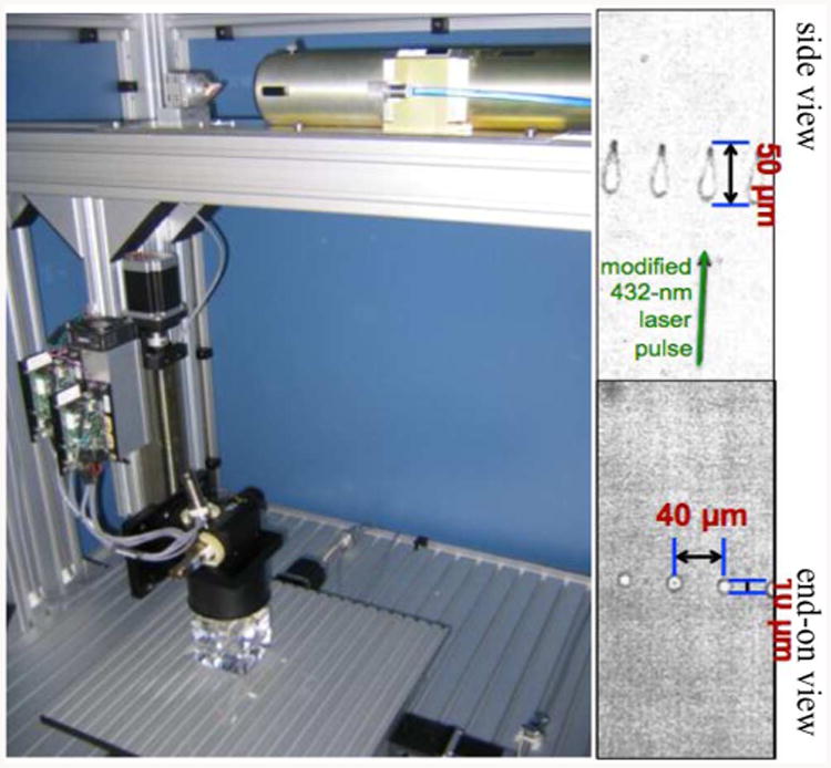
To increase depth sensitivity of an SSLE-dMiCE crystal further, we plan to vary the defect pattern, density, and shape at the interface. However, with our current SSLE system, we are unable to increase point density further without causing macroscopic fractures, which would affect light distribution or compromise crystal integrity. Therefore, we are currently working with Crystalix Evolution GmbH to manufacture a SSLE system (Fig. 31) with optimized optics and laser pulse characteristics to minimize collateral damage in the crystal that would enable us to decrease point spacing and increase optical density in our future SSLE work.
Furthermore, with better control of SSLE defect shape (fewer cracks) we anticipate less light absorption and better energy resolution farther from the photodetectors. Energy resolution is of particular importance for first-interaction positioning, an area of interest we are pursuing for a system of dMiCE crystal arrays.
As we gather more data on the impact of different patterns on performance using the improved SSLE, we will also extend our optical modeling tool (SCOUT) with models of the induced defects. We will then use SCOUT simulations to explore potential defect patterns and surface treatments of the crystal outer surfaces. We will then use the most promising solutions with crystals processed with the improved SSLE system.
Fig. 6.
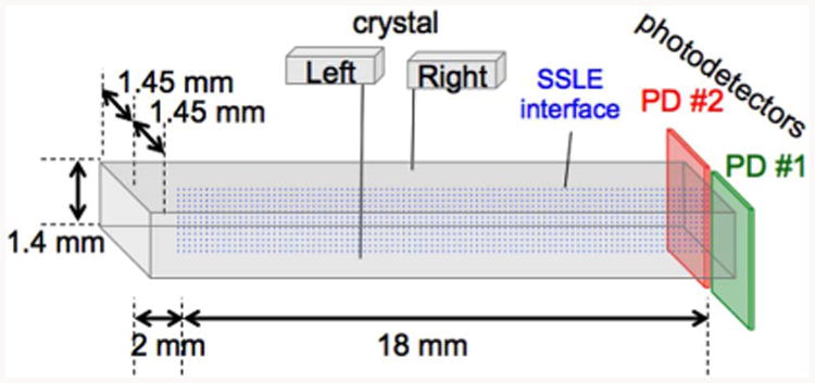
SSLE-dMiCE crystal design examined in this work.
Fig. 22.
Depth-estimate distribution for five beam positions in sample 1b (1-layer SSLE, 140 – μm grid).
Fig. 23.
Depth-estimate distribution for five beam positions in sample 1c (1-layer SSLE, 120 – μm grid).
Fig. 24.
Depth-estimate distribution for five beam positions in sample 2a (2-layer SSLE, 120 – μmgrid).
Fig. 25.
Depth-estimate distribution for five beam positions in sample 2b (2-layer SSLE,120 – μm grid).
Acknowledgments
This work was supported in part by the by NIH Grants NCI CA136569 and NIBIB EB002117.
Footnotes
Color versions of one or more of the figures in this paper are available online at http://ieeexplore.ieee.org.
Digital Object Identifier 10.1109/TNS.2014.2374075
Contributor Information
William C. J. Hunter, Email: wcjh@u.washington.edu, Department of Radiology, University of Washington, Seattle, WA 98195 USA.
Robert S. Miyaoka, Email: rmiyaoka@u.washington.edu, Department of Radiology, University of Washington, Seattle, WA 98195 USA.
Lawrence MacDonald, Email: macdon@u.washington.edu, Department of Radiology, University of Washington, Seattle, WA 98195 USA.
Wendy McDougald, Email: wam2@u.washington.edu, Department of Radiology, University of Washington, Seattle, WA 98195 USA.
Thomas K. Lewellen, Email: tkldog@u.washington.edu, Departments of Radiology and Electrical Engineering, University of Washington, Seattle, WA 98195 USA.
References
- 1.Lewellen TK, MacDonald LR, Miyaoka RS, McDougald W, Champley K. Proc IEEE Nuclear Science Symp and Medical Imaging Conf Rec. Honolulu, HI, USA: 2007. New directions for dMiCE–a depth-of-interaction detector design for pet scanners; pp. 3795–3802. [DOI] [PMC free article] [PubMed] [Google Scholar]
- 2.Hirano Y, Inadama N, Yoshida E, Nishikido F, Murayama H, Watanabe M, Yamaya T. Potential for reducing the numbers of SiPM readout surfaces of laser-processed X'tal cube PET detectors. Phys Med Biol. 2013;58:1361–1374. doi: 10.1088/0031-9155/58/5/1361. [DOI] [PubMed] [Google Scholar]
- 3.Sabet H, Kudrolli H, Singh B, Nagarkar VV. Fabricating high-resolution and high-sensitivity scintillator arrays using laser induced optical barriers. Proc IEEE Nuclear Science Symp and Medical Imaging Conf Rec; Anaheim, CA, USA. 2012. pp. 4080–4084. [Google Scholar]
- 4.Barrett HH, Hunter WCJ, Miller BW, Moore SK, Chen Y, Furenlid LR. Maximum-likelihood methods for processing signals from gamma-ray detectors. IEEE Trans Nucl Sci. 2009 Jun;56, no. 3:725–735. doi: 10.1109/tns.2009.2015308. [DOI] [PMC free article] [PubMed] [Google Scholar]
- 5.Hunter WCJ, Barrett HH, Muzi JP, McDougald W, Mac-Donald LR, Miyaoka RS, Lewellen TK. SCOUT: a fast monte-carlo modeling tool of scintillation camera. Phys Med Biol. 2013;58:3581–3598. doi: 10.1088/0031-9155/58/11/3581. [DOI] [PMC free article] [PubMed] [Google Scholar]