Abstract
In this paper, we propose a design for a 2D slab photonic crystal (PhC) virus sensor and an associated signal analysis methodology that together enable single-virus detection while rejecting false positives that occur due to non-specific interactions of serum proteins and small molecules with the sensor surface. The slab-PhC design takes advantage of both the optical and geometrical properties of its incorporated structures by physically limiting virus infiltration to only the most sensitive region of the PhC sensor, while allowing simultaneous measurement of both site-selective virus infiltration and non-specific small molecule accumulation across the device. Notably, the proposed sensor transducer is compatible with both standard semiconductor fabrication procedures and lab-on-a-chip style microfluidic delivery systems. 3D finite-difference time-domain electromagnetic field computation results are presented, the outcomes of which indicate that both specific (target) virus capture and non-specific (non-target) binding can be simultaneously measured and discerned from one another. This type of capacity for background-corrected, single-pathogen target detection would provide a new and novel advancement toward sensitive, label-free virus diagnostics.
OCIS codes: (280.1415) Biological sensing and sensors, (230.5298) Photonic crystals, (350.4238) Nanophotonics and photonic crystals, (230.3990) Micro-optical devices, (130.5296) Photonic crystal waveguides, (230.5750) Resonators
1. Introduction
Referencing in optical sensors typically involves the use of parallel structures that either lack recognition elements or are not exposed to target [1], nonreactive microarray spots [2], or completely separate reference chips in some cases. While these referencing methods control for instrument effects (optical drift, temperature changes, etc.), they often do not adequately control for sample effects. In complex mixtures such as serum, the latter can be substantial. Nonspecific binding by serum constituents is viewed as a primary reason for the fact that to date there are no FDA-approved clinical assays using surface plasmon resonance (SPR), despite its status as one of the most widely used and extensively studied label-free sensor platforms [3]. Thus, a major challenge in the development of label-free sensors is that of differentiating specific capture of the target of interest from nonspecific adsorption of other materials in the sample being analyzed. Several strategies have been pursued in an effort to address this problem, including the development of a broad range of antifouling coatings [4] and the use of multiple capture areas or antibodies to different epitopes of the target biomolecule [5] for redundant detection. Alternative strategies continue to be desirable, however.
Photonic crystals are structures in which domains of alternating refractive index (RI) in one, two, or three dimensions produce a photonic band gap. The two-dimensional version of this structure (2D slab-PhC) has recently emerged as an object of study for its potential in microscale label-free biosensing [6,7]. Typically fabricated in silicon-on-insulator (SOI) materials, 2D slab-PhCs generally consist of a regular array of low-RI holes in the high-RI insulated silicon layer. A particularly intriguing feature of 2D slab-PhCs is that they can be designed and fabricated such that analyte size selection occurs on the device: if sensing of a “large” analyte is desired, a 2D slab-PhC consisting of lattice holes smaller than the analyte and a defect hole larger than the target analyte will limit target capture to the defect hole. While our work to date has focused on monitoring the shift of a resonance produced by a defect “hole” in the 2D PhC [8], other groups have demonstrated that shifts in the band edge are also observable as material infiltrates into the crystal in defect-free structures [9–13]. In the context of assessing the relative merits of these strategies vs. reliance on defect resonance shifts, 3D electromagnetic field simulations we conducted suggest that while uniform capture of material throughout the sensor causes a shift in both the band edge and the defect resonance, selective capture of a particle in the defect is only observable by a shift in the defect resonance. Here we describe detailed computational studies of this phenomenon and assess the possibility that the intrinsic structure of the slab-PhC sensor allows it to differentiate specific from nonspecific binding.
2. Computational methods and system geometry
Like many slab-PhC sensors that are regularly fabricated on silicon-on-insulator (SOI) substrates, the PhC sensor modeled in this analysis (Fig. 1(a) ) was composed of three principle components: a triangular lattice of low-RI holes in a thin high-RI dielectric slab, a W1 waveguide, and a defect structure that supports a point-like localized optical resonance. This particular choice of geometry follows from previous work by Guillermain and Fauchet [14] and was selected for reasons discussed below. To obtain a complete picture of the photonic properties of both the individual components and their combined implementation, both time-domain and frequency-domain computational methods were employed. Since the computational methods used in this analysis rely on Maxwell’s equations, which are scale invariant, all geometric parameters in the simulations were scaled to the PhC lattice constant - the distance between the centers of two adjacent cylindrical holes in the triangular lattice (denoted a). Frequency (f) and wave vector (kx) thus have scaled units of c/a and 2π/a, respectively (where c denotes the speed of light).
Fig. 1.
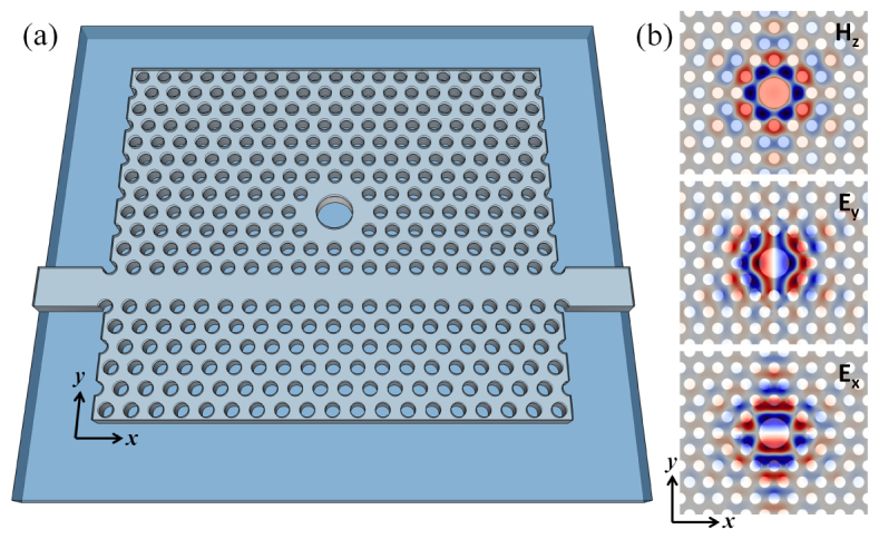
(a) Schematic representation of simulated slab-PhC sensor design, including the patterned top oxide and device layers, supported by a planar buried oxide layer. (b) Electromagnetic field profiles for the optical mode resonance used for sensing. Cross sections are taken at the center plane of the high-RI device layer and demonstrate that the field strength is localized in and around the large-hole defect of PhC. Because of required periodic boundary conditions for the method, the W1 waveguide was not included in the geometry for frequency-domain computation. The waveguide was included for FDTD calculations.
A range of computational cell domains was required to perform the various simulations, but some geometrical properties were common to all of them. All simulations were performed using 3-dimensional computational domains. The thickness of the patterned silicon layer in these simulations was 0.6a. The buried oxide layer below the silicon layer was planar (not patterned), and although a suspended slab-PhC geometry is not analyzed here, the critical behaviors that are being presented are preserved in suspended slab-PhC sensors. A top-oxide hard-mask layer with a thickness of 0.2a covered the device-silicon layer and shared the PhC pattern of the silicon below it. This top oxide layer was included in the simulations for two reasons: first, this type of layer is commonly used as a gas-etch mask during typicalfabrication processes, and second, the top oxide reduces the vertical mode asymmetry that exists in the slab-PhC due to the underlying buried oxide. The cylindrical lattice holes that perforated the silicon and top-oxide layers of the PhC had a radius of 0.3a. Water was the cover material chosen for all simulations because such a slab-PhC sensor is intended for integration with microfluidic channels for material delivery in a lab-on-a-chip device. The critical background-subtraction behaviors being presented here will also exist for slab-PhC sensors that are used in a dried-chip, end-point assay format where air is the cover medium. The refractive indices used for silicon, silicon oxide, water, and biomaterial were 3.480, 1.444, 1.320, and 1.450 (for λ ≈1500 nm).
Frequency-domain calculations were employed to calculate the field profiles and resonance frequency of the point-like defect in an otherwise uninterrupted triangular PhC lattice (using MPB software [15]). The supercell for those computations spanned 10a in the x-direction (Γ-K), (10 rows) in the y-direction, and 2.8a in the z-direction (perpendicular to the plane). The extent of the computational domain in the x- and y-directions was constrained in this case to limit computation times. The defect structure was created by replacing the center lattice hole and its six nearest neighbor holes with a single large cylindrical hole of radius 0.8a. The PhC eigenmode resonance used for sensing is plotted as a horizontal line on the dispersion curve (Fig. 2 ), at f = 0.2617. The simulated geometry and field profiles are displayed in Fig. 1.
Fig. 2.
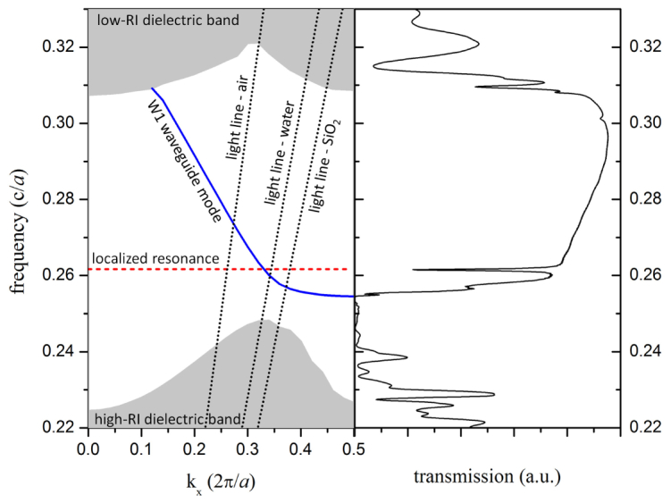
Dispersion diagram (left) and optical transmission spectrum (right) for the slab-PhC sensor design, as computed using FDTD methods.
The dispersion diagrams presented here were calculated with finite-difference time-domain (FDTD) methods [16] (using the Meep software package [17]). To generate dispersion plots, a rectangular W1 waveguide supercell that spanned a single lattice constant of the PhC sensor in the x-direction (Γ-K), (19 rows) in the y-direction, and 2.8a in the z-direction (perpendicular to the plane) was used. Bloch boundary conditions were applied in the x-direction, while perfectly-matched-layer (PML) boundary conditions were applied in the y- and z-directions. The cell was excited with a field pulse of a particular normalized wave vector, kx, over a broad range of frequencies (Gaussian), and the frequency spectrum was then analyzed for eigenmodes [18]. The process was repeated for various 0 < kx < 0.5. To match the symmetry of the fundamental waveguide mode in the input ridge waveguide, only the odd modes (in y-axis) were considered. Figure 2 (left side) displays the dispersion diagram for the system.
Transmission spectra for the full PhC sensor geometry were also modeled using FDTD methods. The simulated geometry consisted of a point-like large-defect cavity side-coupled to a W1 waveguide, as shown in Fig. 1(a). The PhC spanned a length of 19a in the Γ-K direction, and just over (19 rows) in the perpendicular direction. The W1 waveguide was created by removing one row of holes along the Γ-K direction, at the ends of which rectangular ridge waveguides (width = ) were butt coupled for optical signal input/output. The large-hole defect structure was again created by replacing one lattice hole and its six nearest neighbor holes with a much larger cylindrical hole of radius 0.8a. The defect structure was centered four rows from the W1 waveguide in these simulations, although the critical behaviors would again be preserved for greater separation between the defect and W1 waveguide structures. PML boundary conditions were applied at all boundaries. Transmission spectra were calculated by exciting the ridge waveguide with a broad-frequency pulse, allowing the fields to evolve long after the initial pulse passed through the PhC, and then by performing Fourier analysis on the transmitted field flux through the output ridge waveguide [18]. All transmission spectra were normalized against the transmission spectrum of a plain ridge waveguide of the same length. The transmission spectrum for an unmodified sensor is shown in Fig. 2 (right side). In order to verify that the resonant optical mode calculated in FDTD simulations matched the mode calculated using frequency domain methods (Fig. 1(b)), field profiles (not shown) were also computed at the resonant frequency by exciting the input waveguide with a single continuous-wave source for a time span that allowed sufficient electromagnetic field strength accumulation. The mode profiles were in agreement for the two different computational methods.
In computations where material infiltration in the PhC sensor was simulated, two basic geometry alterations were explored. Non-specific adsorption of proteins and small molecules was modeled as a uniform monolayer coating the inside surfaces of all PhC lattice holes, including the defect structure. To model the specific capture of a virus-like pathogen in the large defect structure of the PhC, a sphere of radius 0.3a was placed against the side wall of the defect. A radius of 0.3a was specifically chosen because it represents the minimum size of pathogen that would be physically excluded from infiltrating the non-defect lattice holes of the PhC sensor, thus taking advantage of a design-inherent size-exclusion capability that would help in reducing false positives. Larger pathogens with a radius not exceeding 1.6a could also infiltrate the large-defect hole of the sensor, and would cause an even greater resonance change for detection purposes.
All simulations were run on a parallel computing network with various resource requirements depending on model complexity. A grid resolution of 20 grid points per lattice constant was used for the dispersion relation simulations and for the transmission spectrum in Fig. 2. The frequency-domain calculations used to calculate the mode profiles shown in Fig. 1 had a computational resolution of 32 grid points per lattice constant. Individual simulations completed within hours on 24-48 processors. The remaining transmission spectrum calculations presented below were executed with a computational grid resolution of 50 grid points per lattice constant. For each simulated infiltration geometry, computation completed in around 2.5 days using 96 processors.
3. Results
Plotting the simulated transmission spectrum alongside the dispersion curves for an unmodified PhC sensor, as shown in Fig. 2, facilitates interpretation of the spectral features that are exhibited in the transmission spectrum. The dispersion diagram includes plots of the light lines for bulk air, water, and SiO2, below which guided modes may exist and above which light can couple into the external media. Extended TE-like PhC slab modes are described by the regions at the bottom and top of the diagram, which are commonly referred to as the high-RI dielectric and low-RI dielectric bands, respectively [19]. The region between the high-RI and low-RI dielectric bands in which extended slab modes are prohibited is the photonic band gap. A W1 waveguide mode is plotted within the band gap, and it describes both guided modes (below the light line) and guided resonances (above the light line). The dominant mode resonance of the large-defect cavity is plotted as a horizontal line in the dispersion diagram.
Many of the features observed in the transmission spectrum are directly related to features in the dispersion diagram. Beginning at the low-frequency end of the transmission spectrum, there is limited transmission for f < 0.245. This transmission is attributed to slab modes without excessive lateral losses that also couple to the ridge waveguides with modest efficiency [20]. There is nearly no transmitted field for 0.245 < f < 0.255, frequencies that are within the photonic band gap but which do not overlap a W1 waveguide mode. Transmission rises significantly near f ≈0.255, where the W1 waveguide guided mode intersects the edge of the Brillouin zone in the dispersion diagram. There is a significant dip in transmission around f ≈0.262, due to strong coupling to the optical resonance of the large-defect cavity at that frequency. For frequencies in which the W1 waveguide mode is above the light line (0.257 < f < 0.308), there is still a significant amount of transmission. Although light is able to couple to radiative modes in the substrate and cover region, the index contrast is still relatively large and the losses are low enough that significant transmission is still achieved. Note that the relatively short length of the W1 waveguide (19a) contributes to the reasonable transmission in this frequency range where much longer PhC waveguides would exhibit poor transmission [20]. Transmission begins to drop again around f ≈0.309. Two different phenomena have been reported to explain the cause of the high-frequency transmission band edge for W1 PhCwaveguides, but calculating and comparing both the dispersion curves and the transmission spectrum allow a determination of which is in effect. If the band gap is large enough, the drop in transmission can result from the intersection of the W1 waveguide mode with the Γ-point in the Brillouin zone (vertically transmitted light) [20]. In other cases, including this one, the drop in transmission coincides with the intersection of the W1 waveguide mode with the extended slab mode continuum of the low-RI dielectric band. For increasing frequency, the transmission dips to a local minimum at f ≈0.31, rises again to a local maximum before falling to another minimum around f ≈0.315. While the low-RI dielectric band region is actually a continuum of modes, the minima coincide with anti-crossings [21] between longer lifetime guided resonances within the continuum. More generally, some transmission exists for frequencies overlapping the low-RI dielectric band, due to either W1 guided resonances, coupling to slab modes, or a combination of the two.
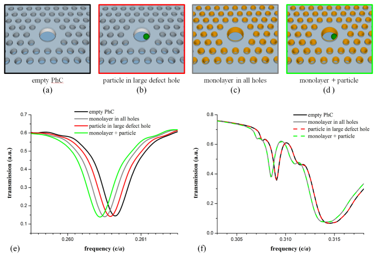
Figure 3 displays the transmission spectra that were calculated for several different instances of material infiltration into the PhC sensor. In addition to the empty PhC sensor (no biomaterial), the three additional infiltration schemes considered were: the case where a single spherical target (simulating a virus) had infiltrated the large-defect cavity, the case where a uniform monolayer of material existed on the walls of all PhC holes, and the combination of the two. Using the empty PhC as the baseline, the resonance changes for the three infiltration schemes were 0.026%, 0.055%, and 0.078% of the initial resonance frequency, respectively. Since these sensors are fabricated in silicon, if the baseline resonance was at a wavelength of 1550 nm, the infiltration events would yield respective shifts of 0.40 nm, 0.85 nm, and 1.21 nm. The high-frequency transmission band edge also exhibited a redshift when the monolayer coating was added to the walls of all PhC holes. However, no redshift in the high-frequency transmission band edge resulted from the infiltration of a single spherical target in the large-defect cavity, regardless of whether the monolayer was present or not. This behavior is important for discerning between non-specific binding of small-molecules and target-specific infiltration of a virus-like particle, as is discussed in the next section. Figure 4 shows how both the localized mode resonance and the high-frequency band edge change in response to the presence of monolayers of increasing thickness on all walls of the PhC holes. As expected, both features experience increasing redshift as the monolayer thickness increases.
Fig. 3.
Various infiltration schemes of material into the slab-PhC sensor (a-d) for which optical spectra (e,f) were simulated using FDTD methods. (a-d) The green sphere in the large-hole defect represents a virus-like particle with radius of 0.3a, the smallest particle for which infiltration into non-lattice PhC holes cannot occur. Orange cylindrical shells represent an aggregated layer of bound small-molecules (thickness of a/50). (e) The shift in frequency for the optical resonance that is localized to the large-defect structure depends on both particle infiltration and small-molecule accumulation. (f) The high-frequency band edge shifts due to the presence of an accumulated material monolayer, but is insensitive to the presence of the virus particle in the large-hole defect.
Fig. 4.
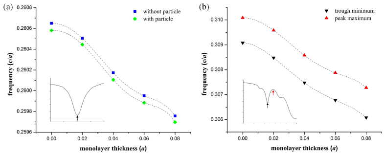
Dependence of features in the optical transmission spectrum on infiltration schemes within the slab-PhC sensor. Monolayer thickness and particle infiltration arrangements correspond to the schematic images in Fig. 3(a-d). Arrows on the inset graphs show where minima/maxima are selected. (a) Frequencies for the optical mode localized to the large-hole PhC defect. (b) Frequencies of the trough and peak spectrum features found in the high-frequency transmission band edge. The two features exhibit the same trend; both are shown to demonstrate flexibility in the selection of the band-edge feature. (a,b) Dashed lines indicate polynomial fits to each data set (R2 = 1).
Additionally, the dispersion relation calculations shown in Fig. 5 demonstrate the sensitivity of the band structure to monolayer accumulation. While the low-frequency cut-off for the W1 waveguide mode shifts downward with increasing monolayer thickness, the lower edge of the low-RI extended mode band is much more strongly affected.
Fig. 5.
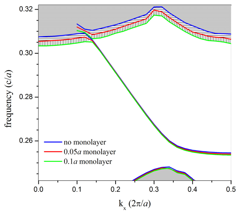
Dispersion diagrams corresponding to different monolayer thicknesses on the sidewalls of PhC lattice holes. Note that the lower boundary of the low-RI dielectric band is the feature most strongly affected by monolayer accumulation.
4. Discussion
The optical transmission properties of a slab-PhC structure at any given frequency are dependent on the refractive indices and geometry of the PhC, the cover medium, and material carried in that medium that has infiltrated the holes of the PhC. This is the core principle that enables the use of slab-PhCs as transducers in biochemical sensing applications. While exact analytical solutions cannot be derived for most PhC geometries, a standard result derived from perturbation theory [19] describes how optical eigenfrequencies shift in response to perturbative refractive index changes:
| (1) |
where ε(r) is the dielectric function and n is the refractive index (ε ≈n2 for lossless materials). This equation indicates that the shift in frequency for a particular feature in the transmission spectrum is proportional to both the refractive index change and the volumetric overlap of electromagnetic field with the space where that change occurs. For the optical resonance that is localized at the point-like defect, field strength is greatest inside and around the large-hole cylinder. The resonant frequency for that mode is thus most sensitive to material infiltration in that large-hole defect itself, whether that infiltration comes in the form of small-molecule adsorption or virus particle capture. The simulation results presented above verified that resonance shifts for that mode occurred in both those situations. For frequencies above the photonic band gap, the presence of delocalized slab modes dominated the transmission properties of the device. At those frequencies, the electric field is distributed more uniformly across the entire lattice of the PhC. The transmission band cut-off is thus affected by the accumulation of material on the side walls of all PhC holes collectively, but is insensitive to isolated capture events that occur in the large-hole defect where only a small fraction of the total field energy resides at that frequency.
To achieve label-free optical detection of a single virus particle capture event in the large-defect hole, the amount of resonance change that occurs for the localized cavity mode must be differentiated from the contribution to the resonance change that comes from the non-specific accumulation of small molecules across the entire sensor. This task can be performed by simultaneously analyzing spectral information from both the localized resonant mode and the high-frequency band edge. By combining red-shift information for those two different sections of the transmission spectrum, it is possible to decouple the amount of resonance shift that results from each of the two interactions. As shown in Fig. 4, functions can be fit to the resonance changes that occur both at the band edge and for the localized resonance to calibrate for small-molecule binding. The specific fitting function itself is not important, so long as it is composed of a series of linearly independent terms that span the variable space. As an example, consider the system of equations that decomposes resonance shifts onto the polynomial basis:
| (2) |
| (3) |
where x represents monolayer thickness, y represents the average resonance shift due to a single virus particle in the large-defect hole, m denotes the number of captured virus particles, and Δfbe and Δfdef denote the frequency redshifts for a selected transmission band edge feature and the localized optical resonance, respectively. The coefficients cj and dk can be determined empirically through simulation or by experimentally detecting different monolayer thicknesses that result from non-specific binding of small molecules. Likewise, the single-particle resonance shift, y, can also be determined empirically either through simulation or a careful control experiment. Following these calibration tasks, the system of equations could be solved for m, the number of virus particles in the large-defect hole, given experimental data for the pair of spectral feature shifts Δfbe and Δfdef. This large-defect PhC transduction platform would therefore be capable of background-corrected single-pathogen target detection.
It must be noted that this capability also relies on the size-exclusion filtering that is inherent in the large-defect PhC sensor design, where the target of interest must be large enough that it does not penetrate into the non-defect lattice holes. Because of this geometric constraint, the background-subtracted resonance change can only come from penetration of the target pathogen into the large-hole defect. For other PhC designs without that geometrical constraint, background corrected detection of a single pathogen at a particular location is still possible, but without the certainty that the background-subtracted resonance change results from only one pathogen within the entire PhC sensor.
5. Conclusion
In this paper, we proposed a design for a photonic virus sensor and an associated signal analysis methodology that together enable single-virus detection while rejecting false positives that occur due to non-specific interactions of serum proteins and other small molecules with the sensor surface. The PhC design takes advantage of both the optical and geometrical properties of its incorporated structures, namely a large-hole cavity and a W1 waveguide. The existence of a sensitive optical mode resonance in the large-hole cavity enables detection of material infiltration, while the size difference between the large-hole cavity and surrounding PhC lattice holes selectively inhibits viruses from infiltrating the insensitive region of the sensor. Specific virus capture can of course be enhanced further by antibody mediated recognition, as we have demonstrated in experimental work [8]. The optical transmission properties of the W1 waveguide permit measurement of nonspecific small-molecule binding, and also allow the incorporation of multiple sensing cavities in series along a single waveguide for redundant or multiplexed detection. The proposed sensor transducer is compatible with standard semiconductor fabrication procedures and could be manufactured on a large scale at reasonable costs. Additionally, it is compatible with microfluidic environments for lab-on-a-chip implementation.
We presented finite-difference time-domain electromagnetic field computation results, including dispersion band properties and optical transmission spectra, for various schemes of material infiltration in the slab-PhC sensor. The simulated outcomes indicate that both virus capture and small-molecule binding can be simultaneously measured and discerned from one another. This type of capacity for background-corrected, single-pathogen target detection is an accomplishment that has not been realized, to our knowledge, using any existing sensing modality.
Acknowledgments
We thank the University of Rochester’s Health Sciences Center for Computational Innovation (HSCCI) and Center for Integrated Research Computing (CIRC) for providing computing systems and support that enabled this computational research. This work was supported by the National Institutes of Health (NIAMS T32AR007472, NIAID R01AI08077).
References and links
- 1.Zhang M., Ge C., Lu M., Zhang Z., Cunningham B. T., “A self-referencing biosensor based upon a dual-mode external cavity laser,” Appl. Phys. Lett. 102(21), 213701 (2013). 10.1063/1.4801427 [DOI] [PMC free article] [PubMed] [Google Scholar]
- 2.Carter J. A., Mehta S. D., Mungillo M. V., Striemer C. C., Miller B. L., “Analysis of inflammatory biomarkers by Arrayed Imaging Reflectometry,” Biosens. Bioelectron. 26(9), 3944–3948 (2011). 10.1016/j.bios.2011.02.025 [DOI] [PMC free article] [PubMed] [Google Scholar]
- 3.Simon A. B., Leung B. M., Bersano-Begey T., Bischof L., Takayama S., “Pathology: Chemical Tests,” in The Physiological Measurement Handbook, Webster J. G., ed. (CRC Press, 2015), pp. 370. [Google Scholar]
- 4.Blaszykowski C., Sheikh S., Thompson M., “Surface chemistry to minimize fouling from blood-based fluids,” Chem. Soc. Rev. 41(17), 5599–5612 (2012). 10.1039/c2cs35170f [DOI] [PubMed] [Google Scholar]
- 5.Lundberg M., Eriksson A., Tran B., Assarsson E., Fredriksson S., “Homogeneous antibody-based proximity extension assays provide sensitive and specific detection of low-abundant proteins in human blood,” Nucleic Acids Res. 39(15), e102 (2011). 10.1093/nar/gkr424 [DOI] [PMC free article] [PubMed] [Google Scholar]
- 6.Pal S., Fauchet P. M., Miller B. L., “1-D and 2-D photonic crystals as optical methods for amplifying biomolecular recognition,” Anal. Chem. 84(21), 8900–8908 (2012). [DOI] [PMC free article] [PubMed] [Google Scholar]
- 7.Baker J. E., Sriram R., Miller B. L., “Two-dimensional photonic crystals for sensitive microscale chemical and biochemical sensing,” Lab Chip 15(4), 971–990 (2015). 10.1039/C4LC01208A [DOI] [PMC free article] [PubMed] [Google Scholar]
- 8.Pal S., Yadav A. R., Lifson M. A., Baker J. E., Fauchet P. M., Miller B. L., “Selective virus detection in complex sample matrices with photonic crystal optical cavities,” Biosens. Bioelectron. 44, 229–234 (2013). 10.1016/j.bios.2013.01.004 [DOI] [PMC free article] [PubMed] [Google Scholar]
- 9.Skivesen N., Têtu A., Kristensen M., Kjems J., Frandsen L. H., Borel P. I., “Photonic-crystal waveguide biosensor,” Opt. Express 15(6), 3169–3176 (2007). 10.1364/OE.15.003169 [DOI] [PubMed] [Google Scholar]
- 10.Buswell S. C., Wright V. A., Buriak J. M., Van V., Evoy S., “Specific detection of proteins using photonic crystal waveguides,” Opt. Express 16(20), 15949–15957 (2008). [DOI] [PubMed] [Google Scholar]
- 11.Baker S. E., Pocha M. D., Chang A. S. P., Sirbuly D. J., Cabrini S., Dhuey S. D., Bond T. C., Létant S. E., “Detection of bio-organism simulants using random binding on a defect-free photonic crystal,” Appl. Phys. Lett. 97(11), 113701 (2010). 10.1063/1.3487998 [DOI] [Google Scholar]
- 12.Toccafondo V., García-Rupérez J., Bañuls M. J., Griol A., Castelló J. G., Peransi-Llopis S., Maquieira A., “Single-strand DNA detection using a planar photonic-crystal-waveguide-based sensor,” Opt. Lett. 35(21), 3673–3675 (2010). 10.1364/OL.35.003673 [DOI] [PubMed] [Google Scholar]
- 13.García-Rupérez J., Toccafondo V., Bañuls M. J., Castelló J. G., Griol A., Peransi-Llopis S., Maquieira Á., “Label-free antibody detection using band edge fringes in SOI planar photonic crystal waveguides in the slow-light regime,” Opt. Express 18(23), 24276–24286 (2010). 10.1364/OE.18.024276 [DOI] [PubMed] [Google Scholar]
- 14.Guillermain E., Fauchet P. M., “Multi-channel biodetection via resonant microcavities coupled to a photonic crystal waveguide,” Proc. SPIE 7167, 71670D (2009). 10.1117/12.808008 [DOI] [Google Scholar]
- 15.Johnson S., Joannopoulos J., “Block-iterative frequency-domain methods for Maxwell’s equations in a planewave basis,” Opt. Express 8(3), 173–190 (2001). 10.1364/OE.8.000173 [DOI] [PubMed] [Google Scholar]
- 16.Taflove A., Hagness S. C., Computational Electrodynamics: The Finite-Difference Time-Domain Method, 3rd ed. (Artech House, Inc, 2005). [Google Scholar]
- 17.Oskooi A. F., Roundy D., Ibanescu M., Bermel P., Joannopoulos J. D., Johnson S. G., “Meep: A flexible free-software package for electromagnetic simulations by the FDTD method,” Comput. Phys. Commun. 181(3), 687–702 (2010). 10.1016/j.cpc.2009.11.008 [DOI] [Google Scholar]
- 18.Mandelshtam V. A., Taylor H. S., “Harmonic inversion of time signals and its applications,” J. Chem. Phys. 107(17), 6756–6769 (1997). 10.1063/1.475324 [DOI] [Google Scholar]
- 19.J. D. Joannopoulos, S. G. Johnson, J. N. Winn, and R. D. Meade, Photonic Crystals: Molding the Flow of Light, 2nd ed. (Princeton University, (2008). [Google Scholar]
- 20.McNab S., Moll N., Vlasov Y., “Ultra-low loss photonic integrated circuit with membrane-type photonic crystal waveguides,” Opt. Express 11(22), 2927–2939 (2003). 10.1364/OE.11.002927 [DOI] [PubMed] [Google Scholar]
- 21.Qiu M., Azizi K., Karlsson A., Swillo M., Jaskorzynska B., “Numerical studies of mode gaps and coupling efficiency for line-defect waveguides in two-dimensional photonic crystals,” Phys. Rev. B 64(15), 155113 (2001). 10.1103/PhysRevB.64.155113 [DOI] [Google Scholar]


