Abstract
A template-free precipitation method was used as a simple and low cost method for preparation of CeO2 nanoparticles. The structure and morphology of the prepared nanoparticle samples were studied in detail using X-ray diffraction, Raman spectroscopy and Scanning Electron Microscopy (SEM) measurements. The whole powder pattern modelling (WPPM) method was applied on XRD data to accurately measure the crystalline domain size and their size distribution. The average crystalline domain diameter was found to be 5.2 nm, with a very narrow size distribution. UV-visible absorbance spectrum was used to calculate the optical energy band gap of the prepared CeO2 nanoparticles. The FT-IR spectrum of prepared CeO2 nanoparticles showed absorption bands at 400 cm-1 to 450 cm-1 regime, which correspond to CeO2 stretching vibration. The dielectric constant (εr) and dielectric loss (tan δ) values of sintered CeO2 compact consolidated from prepared nanoparticles were measured at different temperatures in the range from 298 K (room temperature) to 623 K, and at different frequencies from 1 kHz to 1 MHz.
Introduction
Nanomaterials have attracted considerable attention in a broad range of advanced applications in multidisciplinary fields including material science and biology, based on the chemical composition, size, shape and surface dependent properties of nanoparticles [1,2]. It is well known that material properties changes when (i) particle size reduces to nano-scale or (ii) materials transferred to nanostructures form, leading to recent advances in synthesis of nanostructures [3]. The particle size of materials affects their basic properties such as lattice symmetry, cell parameters, and structural characteristics. Generally, phases in bulk form are unstable in bulk material due to high surface energy, however the surface energy decreases rapidly when size reduces to nanoscale level leading to high stability of materials at nanostructure levels [3,4].
Cerium (Ce) is one of the most abundant rare earth elements of the lanthanide series in earth’s crust and is present at about 66 ppm as a free metal and/or oxide forms. The two main oxidation sates of cerium are ceric- Ce (IV) and cerous- Ce (III), and can auto regenerate () [5]. Both oxidation sates of Ce show strong absorbance peaks in ultraviolet light wavelength in the range at ~ 230–260 nm and at ~ 300–400 nm corresponding to Ce (III) and Ce (IV) oxidation states of cerium, respectively [6]. Materials containing Ce are widely used in the field of metallurgy, ceramics, and smart glasses and in optics. Cerium oxide nanoparticles (CNPs) have been widely utilized in various advanced technologies, such as solid-oxide fuel cells, high-temperature oxidation protection materials, catalytic materials, oxygen sensors and solar cells, etc [7–9]. When the size of cerium oxide reduces to nanometre scale, it shows exceptional properties including increase of optical band gap of nanoceria as a result of the quantum size effect at nanometre scale. Nanoparticle form of cerium shows remarkable catalytic reactivity due to high mobility of surface oxygen vacancies [10]. These oxygen vacancies alter the electronic and valence arrangement, which fix the oxidation state. CeO2 nanoparticles have also been used as a free radical scavenger, to modulate oxidative stress in biological system [11]. For example, CeO2 nanoparticles are able to rescue HT22 cells from oxidative stress-induced cell death, and protect normal human breast cells from radiation-induced apoptotic cell death [11,12]. In fluorite structure, CeO2 has a stable structure over a wide range of temperature in its pure stoichiometric form and the structure remains unchanged. Furthermore, CeO2 has also been regarded as a possible gate dielectric material in metal-oxide-semiconductor and memory devices for next generation devices [13–15]. This is because CeO2 has high ability for oxygen storage which makes CeO2 as one of the most important automobile exhaust catalysts [16].
Various chemical route methods have been reported on the synthesis of CeO2 oxide nanoparticles such as reversed micelles route, co-precipitation, hydrothermal synthesis, forced hydrolysis, solvo-thermal synthesis, sol–gel process, pyrolysis, electrochemical method, and sono-chemical methods [17–26]. In this work, we report on synthesis of CeO2 nanoparticles by a facile and single one-pot template-free precipitation route without any need of capping ligands and other additives. The structural, optical and dielectric properties of the prepared CeO2 nanoparticles samples have been systematically investigated.
Material and Methods
Synthesize and characterization of CeO2 nanoparticles
CeO2 nanoparticles were prepared by a wet chemical precipitation method. Firstly, (30 mmol) of Ce(NO3)3.6H2O (Aldrich, Germany) was dissolved in distilled water. The dissolved solution was then added drop wise into a beaker containing 100 mL of 0.4M NaOH (Merck, Germany) solution at room temperature. The pH value of the solutions during experiment was maintained constant to around 13. At this pH, precipitates immediately formed and were then ultra-centrifuged at a speed of 10,000 rpm for 10 min to obtain clear supernatant liquids separated from precipitates. The centrifuged precipitates were further washed several times with distilled water to complete removal of unwanted Na+, Cl-, NO3 - ions. The washed precipitates were then dried at 353 K for 3 h.
The crystallinity of the prepared nanoparticles samples was studied by measuring powder X-ray diffraction (XRD) pattern using Panalytical X’Pert Pro, NL diffractometer in θ/θ geometry, equipped with a fast RTMS detector, with Cu Kα (1.54 Å) radiation (45 kV and 40 mA, 2θ range from 20–125° with a virtual step scan of 0.1° and virtual time per step of 500 s). The incident beam pathway was: 0.5° divergence slit, 0.5° anti-scattering slit, 0.04 rad soller slits, and a 15 mm copper mask. The pathway of the diffracted beam included a Ni filter, soller slits (0.04 rad), and an anti-scatter blade (5 mm).
The microstructure topography and chemical analysis of the samples was studied using scanning electron microscopy (SEM, SU-70, Hitachi) and by measuring in-situ energy-dispersive X-ray spectroscopy (EDS) patterns, respectively. To prevent the charge build up during SEM observations, samples were coated with carbon. HITACHI SU-70 high resolution transmission electron microscope (HRTEM), equipped with a Bruker EDS detector was used to further analyses of the structure of the prepared nanoparticles samples. The optical properties of the samples were measured by using UV–Visible–NIR (Perkin-Elmer, Lambda 35), Raman (laser wavelength 1064 nm; laser power 350 mW) and Fourier transform infrared spectroscopy (FT-IR, Bruker RFS/100) spectrometry. For the measurement of electrical properties, the dried nanoparticles were uniaxially pressed in to disc-shaped pellets of 10 mm diameter using the isostatic pressure of 200 MPa. The pressed samples were sintered at 1273 K for 2 h. Top conductive electrodes were then deposited on both sides of sintered samples using silver paste. Dielectric constant and loss were measured at different temperatures and frequencies in the range of 298 K to 623 K and 100 Hz to 1 MHz respectively, using an impedance analyzer (4294A, Agilent, USA).
Results and Discussion
Structural properties
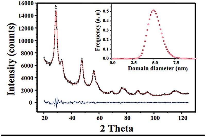
XRD patterns shows cubic phase for prepared CeO2 nanoparticles (Fig 1). Furthermore, the whole powder pattern modelling (WPPM) method [27], taking advantage of the PM2K software [28,29], that allows for refinement of model parameters via a non-linear least squares routine, was employed for the micro structural analysis of CeO2. This procedure is considered to be a state-of-the-art methodology, and allows for the extraction of micro structural information from a diffraction pattern. With such a methodology, the experimental peaks are fitted without the use of any arbitrary analytical functions (i): the diffraction peak profile is the result of a convolution of instrumental and sample-related physical effects. As a consequence, the analysis is directly made in terms of physical models of microstructure and/or lattice defects.
Fig 1. Graphical output of the WPPM modelling of CeO2 (black open squares are the calculated data, red continuous line the observed data, and the lower blue continuous line is the difference curve between observed and calculated profiles).
In the inset is reported ceria crystalline domain size distribution.
Hence, with the WPPM method, aspects of microstructure such as the crystalline domain shape and size distribution can be accurately measured, with a method deeply superior to the estimations made by other frequently used integral breadth methods for line profile analysis (LPA)—i.e. the widely used Scherrer formula [30], or the Williamson–Hall method [31]. Actually, with the use of these quoted methods, it can be tricky to correctly extract integral breadths, because of the instrumental profile component, background and peak profile overlapping. Furthermore, additional sources of line broadening—i.e. domain size, and/or lattice strain—cannot be considered properly by LPA methods [32]. The instrumental contribution was obtained by modelling 14 hkl reflections from the NIST SRM 660b standard (LaB6), according to the Cagliotiet al. relationship [33]. Afterward, CeO2 (fcc, space group (SG) Fm3m) was included in the WPPM modelling. The following parameters were refined: background (modelled using a 5th-order of the shifted Chebyshev polynomial function), peak intensities, specimen displacement, and lattice parameters. In this work, we assumed crystalline domains to be spherical, and distributed according to a lognormal size distribution. The WPPM results obtained for CeO2 samples are shown Table 1. The average crystalline domain diameter of prepared ceria was found to be 5.2 nm, with a very narrow size distribution with maxima centred at ~ 5 nm as depicted in inset of Fig 1. It is also interesting to note that no crystalline domains were detected below ~ 2.5 nm. All the crystalline domains were found in the range in between 2.5 to 7.5 nm.
Table 1. WPPM agreement factors, unit cell parameters and average crystalline domain diameter of CeO2.
| Agreement factors | Unit cell parameters | Average crystalline domain diameter (nm) | Mode of the size distribution (nm) | ||
|---|---|---|---|---|---|
| R wp (%) | R exp (%) | χ 2 | a = b = c (nm) | ||
| 2.85 | 1.81 | 1.57 | 0.5438(1) | 5.2±0.1 | 5.0±0.1 |
Scanning electron microscopy (SEM)
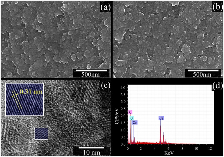
Fig 2a and 2b presents SEM images of the prepared CeO2 nanoparticles. The SEM images reveal synthesis of nano-sized CeO2 particles with an average diameter size of approximately ~25 nm (Fig 2a and 2b). Fig 2c shows HRTEM image obtained for prepared CeO2 nanoparticles. From HRTEM image analysis, the distance between neighbouring planes was measured equal to ~ 0.31 nm, which corresponds to (111) crystallographic plane of cubic CeO2 [34]. The corresponding EDS analysis for the sample is presented in Fig 2d. The presence of O and Ce elements was evident from the measured EDS spectra. No extra impurity was detected in EDS spectrum. The detected C signal was expected as a consequence of signals from conductive carbon tape used for sticking of the powder on the sample holder.
Fig 2.
(a) and (b) SEM images, (c) HRTEM image and (d) EDS analysis of the CeO2 nanoparticle.
Optical properties
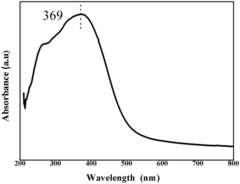
Fig 3 shows the optical absorption spectra of prepared CeO2 nanoparticles in UV-visible range of electromagnetic wavelengths. In ultraviolet absorption process, the outer electrons of atoms or molecules absorb photons and undergo transitions to higher energy levels. Therefore, the obtained optical absorption spectrum can be used to calculate the energy band gap of the CeO2 material. UV-visible spectrum of the CeO2 nanoparticles shows a distinct absorption band at 369 nm. The optical band gap energy of CeO2 nanoparticles was calculated according to Eq (1) given by:
| (1) |
Where, λ is the wavelength (nm) and E bg is the optical band gap energy. The calculated optical band gap value of prepared CeO2 was found to be 3.36 eV, which is larger than that of 3.2 eV, reported in literature for bulk CeO2 [35]. The enhancement in optical band gap of CeO2 nanoparticle could be due to the quantum size effect and is consistent with literature report for CeO2 nanoparticles [36].
Fig 3. UV-Visible absorbance spectrum of prepared CeO2 nanoparticles.
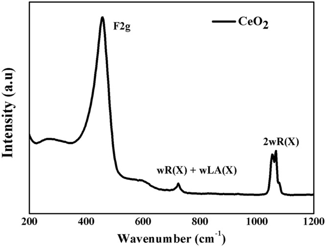
CeO2 belongs to O 5h (Fm3m) space group with cubic fluorite structure. The first order Raman line at around 465 cm-1 attributed to triply degenerate Raman active optical phonon mode (F 2g). The second order Raman spectrum, has nine phonon branches, with 45 possible phonon modes and are located at 580, 660, 880, 1030 and 1160 cm-1 for ωTO(X) + LA(X), ωR(X) + LA(X), ωLO + ωTO, 2ωR(X) and 2ωLO, respectively [16]. Fig 4 indicates the room temperature Raman spectrum of the CeO2 nanoparticles with the fluorite phase measured within a range of 200–1200 cm-1. A first order Raman peak (F2g) at 453 cm-1 and a two second order Raman peaks prominent at 717 and 1050 cm-1 were observed which are in good agreement with the previous reports [37].
Fig 4. Raman spectrum of CeO2 nanoparticles.
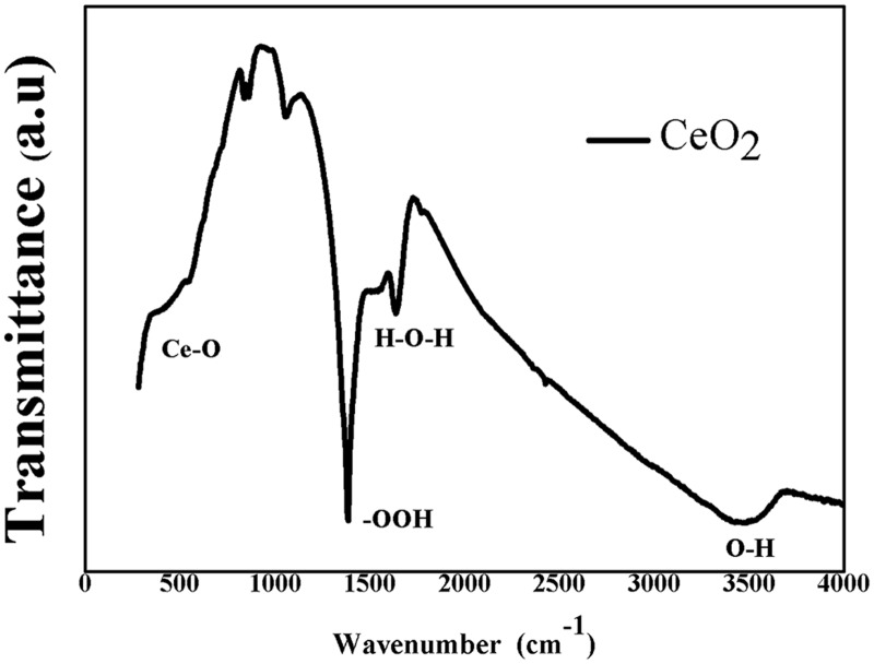
Fig 5 shows the FTIR spectrum of prepared CeO2 nanoparticles. The prepared CeO2 nanoparticles reveals the presence of some absorption bands in the ranges from 400 cm-1 to 4000 cm-1, positioned at 450 cm-1, 1360 cm-1,1630 cm-1, and 3430 cm-1. The absorption band at 450 cm-1 corresponds to CeO2 stretching vibration. The signal at 1630 cm-1 is associated with the molecular H2O (H–O–H) bending frequency [38,39]. The broad adsorption band about 3430 cm-1 corresponds to hydrated and physically adsorbed water in the sample [40].
Fig 5. FT-IR spectrum of CeO2 nanoparticle.
Dielectric properties
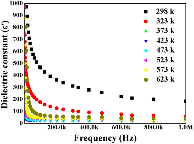
For the electrical characterization, namely dielectric constant (ε r) and dielectric loss (tan δ), the sintering conditions (1273 K for 2 h) that enabled achieving the high dense CeO2 ceramics consolidated from CeO2 nanoparticles were chosen. Fig 6 shows the frequency dispersion of ε r values of prepared CeO2 ceramic, in the range from 1 kHz to 1 MHz measured at various temperatures from 298 K to 623 K. The high ε r values at the low frequencies are because of interfacial or space charge polarisations. The ε r values decreases with increasing frequency and reaches a constant value at higher frequencies. The obtained result is similar with works which were reported for dielectric ZnO nanocrystals [41,42]. Interfacial polarisation or space charge polarisation in CeO2 nanoparticles ceramic is due to the structural in-homogeneity because of large surface-to-volume ratio of nanoparticles. The external electric field causes the space charges move and trapped through the defects at the interfaces leading to formation of dipole moments. The space charge polarisation is dominant at low frequencies and Maxwell-Wagner dielectric dispersion theory is applicable to explain the dielectric behaviour of the sample [43–45]. Therefore, the grain boundaries effect is more pronounced at low frequencies. The electrons/holes hopping between positive and negative surface defect centres in the grain boundary region might constitute the dielectric polarisation at low frequencies. At higher frequencies, the dipoles rotational displacement results in orientational polarisation and with the increase of frequency, the electric dipoles in the material start to lag behind the applied electric field. However, the dielectric constant decreases exponentially and at higher frequencies, the dipoles fail to cope with rapid electric field variations. Therefore, a constant value was obtained for the dielectric constant at higher frequencies. It can also be noted from Fig 6 that, the dielectric constant is considerably decreased with increase in measuring temperature up to temperature of 373 K and thereafter start to increase a little bit with further increase of the temperature. This might be due to reduction of pore space volume between the particles, when the consolidated CeO2 nanoparticles compact was subjected to a high temperature sintering which causes larger grains growth at the expense of smaller grains and reduce of the energy barrier with rapid increase of the diffusion of atoms to another grain. Therefore, the sintered ceramic shows conductor type behaviour due to the increase of conductivity with increase of mobility.
Fig 6. The dielectric constant of the CeO2 nanopowder versus frequency at various temperatures.
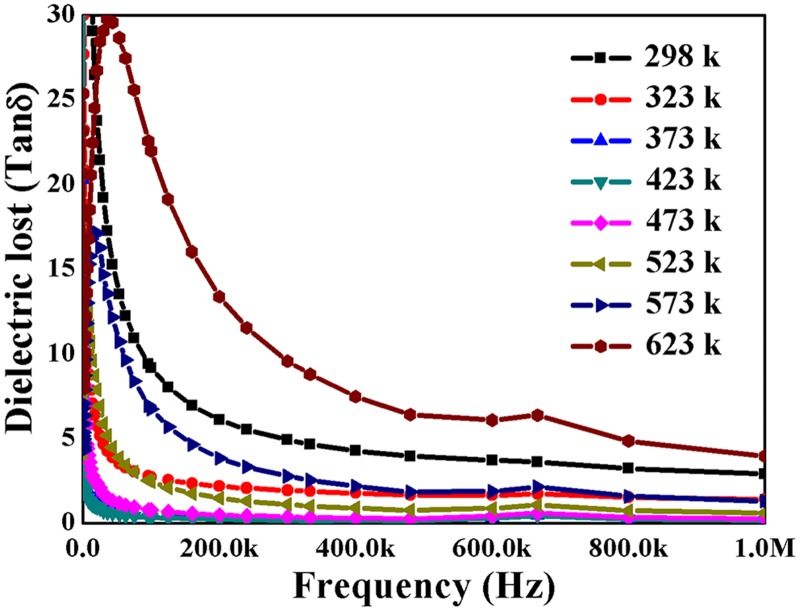
The dielectric loss (tan δ) behaviours against frequency ranging from 1 kHz to 1MHz at various temperatures is shown in Fig 7. The tan δ values were found to decrease with increasing frequency due to the space charge polarization. Generally, the low loss is observed at higher frequencies, because the motion of domain wall is inhibited and magnetization is forced to change rotation. On the other hand the tan δ values were found to decrease with increasing temperatures till 473 K and then start to increase when measured at temperatures higher than473 K. The sintered CeO2 nanoparticles ceramic shows lower values of tan δ at 323 K, 373 K and 423 K when compared to values measured at 298 K (room temperature).
Fig 7. The dielectric loss CeO2 nanoparticles versus frequency of applied field at various temperatures.
This indicates that the CeO2 nanoparticles dielectric ceramic can store more energy due to small loss and shows good dielectric behaviour at these temperatures. While, the tan δ values measured at 623 K were found to be high, revealing material cannot store energy at this temperature. The ac conductivity of the prepared CeO2 sample was further calculated using Eq (2) given by:
| (2) |
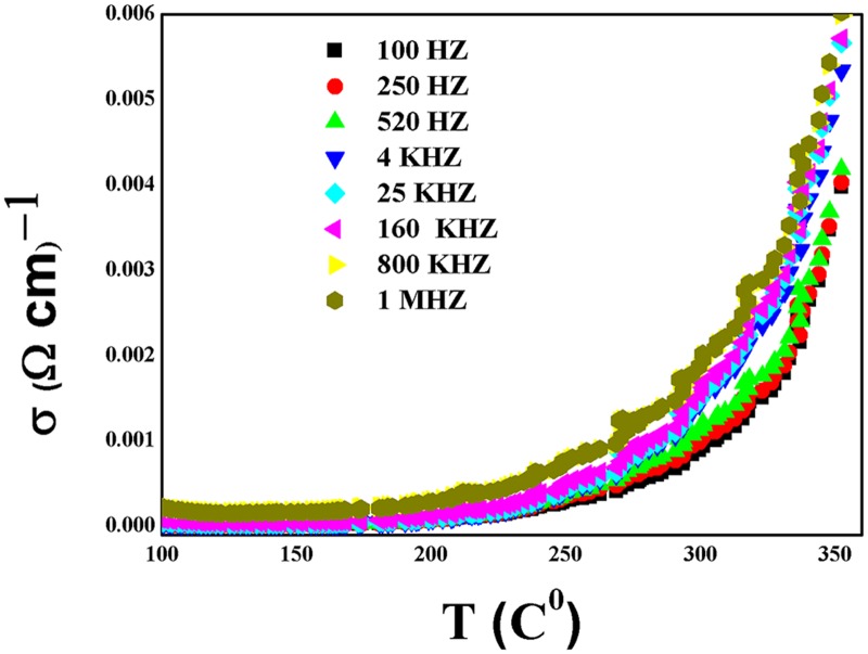
Fig 8 shows the variation of ac conductivity calculated for prepared CeO2 nanoparticles ceramic with temperatures at different frequencies. As the temperature increases, the ac conductivity was found to be constant up to temperature of 450 K, and then increases with further increase in temperatures above 450 K. This behaviour could be due to thermally activated hopping of charge carriers between different localized states. Furthermore, the ac conductivity maximum value increases with increasing frequency, since the immigration of electrons is increased with increase in frequency.
Fig 8. The variation of ac conductivity of CeO2 nanopartciles with temperature at different frequency.
Conclusions
Low cost wet chemical method has been successfully established for the synthesis of CeO2 nanoparticles. The method was found to be convenient, rapid, and efficient in CeO2 nanoparticles synthesis. The average crystalline domain diameter from XRD analysis was found to be 5.2 nm, with a very narrow size distribution. The first order Raman line was obtained at around 465 cm-1 corresponding to triply degenerate Raman active optical phonon mode (F 2g). The high values of dielectric constant for sintered CeO2 nanoparticles compact were observed in low frequencies regions due to structural in-homogeneity which was formed because of large surface-to-volume ratio of nanoparticles. Furthermore, the variations of dielectric constant values with measuring temperatures showed considerable decrease in dielectric constant values with increasing temperatures up to 373 K. Moreover, low loss values were found for prepared CeO2 samples at higher frequencies when measured at 323 K, 373 K and 423 K compared to loss values obtained at 298 K. The ac conductivity measured for prepared CeO2 samples was found to be constant with increase in temperature till 450 K, which further increases with increase in temperature above 450 K.
Acknowledgments
Reza Zamiri would like to thank the Foundation for Science and Technology of Portugal (FCT) and Universiti Putra Malaysia Postdoctoral research fellow program (R.Z.) for the financial support under the grant references, SFRH/BPD/76185/2011 and NSR-8978 (G.P.D.). Ajay Kaushal thanks the financial support under the grant references SFRH/BPD/77598/2011 from the Foundation for Science and Technology of Portugal (FCT). D.M. Tobaldi is grateful to the ECO-SEE project (funding from the European Union’s Seventh Framework Programme for research, technological development and demonstration under grant agreement no 609234. Note: The views expressed are purely those of the authors and may not in any circumstances be regarded as stating an official position of the European Commission). The authors would also like to thank CICECO for the work at the University of Aveiro.
Data Availability
All relevant data are within the paper.
Funding Statement
Reza Zamiri would like to thank the Foundation for Science and Technology of Portugal (FCT) and Universiti Putra Malaysia Postdoctoral research fellow program (Reza Zamiri) for the financial support under the grant references, SFRH/BPD/76185/2011 and NSR-8978 (G. P. D.). Ajay Kaushal thanks the financial support under the grant references SFRH/BPD/77598/2011 from the Foundation for Science and Technology of Portugal (FCT). David M. Tobaldi is grateful to the ECO-SEE project (funding from the European Union’s Seventh Framework Programme for research, technological development and demonstration under grant agreement no 609234. Note: The views expressed are purely those of the authors and may not in any circumstances be regarded as stating an official position of the European Commission). The authors would also like to thank CICECO for the work at the University of Aveiro.
References
- 1. Sehgal A, Lalatonne Y, Berret JF, Morvan M. Precipitation-redispersion of cerium oxide nanoparticles with poly (acrylic acid): Toward stable dispersions. Langmuir 2005; 21: 9359–9364. [DOI] [PubMed] [Google Scholar]
- 2. Lewis JA. Colloidal processing of ceramics. Journal of American Ceramic Soiety 2000; 83: 2341–2359. [Google Scholar]
- 3. Gleiter H. Nanostructured Materials: Basic Concepts and Microstructure. Acta Materialia 2000; 48: 1–29. [Google Scholar]
- 4. Renu G, DivyaRani VVS, Nair V. Subramanian, K.R.V.; Vinoth-Kumar, L. Development of cerium oxide nanoparticles and its cytotoxicity in prostate cancer cells. Advanced Science Letters 2012; 6: 17–25. [Google Scholar]
- 5. Ayyub P, Palkar VR, Chattopadhyay S, Multani M. Effect of crystal size reduction on lattice symmetry and cooperative properties. Physical Review B 1995; 51: 6135–6138. [DOI] [PubMed] [Google Scholar]
- 6. Hu Z, Haneklaus S; Sparovek G, Schnug E.) Rare earth elements in soils. Communications in Soil Science and Plant Analysis 2006; 37: 1381–1420. [Google Scholar]
- 7. Zhang Y, Andersson S, Muhammed M. Nanophase catalytic oxides: I. Synthesis of doped cerium oxides as oxygen storage promoters. Applied Catalysis B: Environmental 1995; 6: 325–337. [Google Scholar]
- 8. Lira-Cantu M, Norrman K, Anderasen JW, Krebs FC. Oxygen release and exchange in niobium oxide MEHPPV hybrid solar cells. Chemistry of Materials 2006; 18: 5684–5690. [Google Scholar]
- 9. Abecassis-Wolfovich M, Jothiramalingam R, Landau Herskowitz MV, Viswanathan B, Varadarajan TK. Cerium incorporated ordered manganese oxide OMS-2 materials: Improved catalysts for wet oxidation of phenol compounds. Applied Catalysis B: Environmental 2005; 59: 91–98. [Google Scholar]
- 10. Brandily-Anne M-L, Lumeau J, Glebova L, Glebov LB. Specific absorption spectra of cerium in multicomponent silicate glasses. Journal of Non-Crystalline Solids 2010; 356: 2337–2343. [Google Scholar]
- 11. Niu J, Azfer A, Rogers LM, Wang X, Kolattukudy PE. Cardioprotective effects of cerium oxide nanoparticles in a transgenic murine model of cardiomyopathy. Cardiovascular Research 2007; 73: 549–559. [DOI] [PMC free article] [PubMed] [Google Scholar]
- 12. Schubert D, Dargusch R, Raitano Chan JSW. Cerium and yttrium oxide nanoparticles are neuroprotective. Biochem. Biophys. Research Communication 2006; 342: 86–91. [DOI] [PubMed] [Google Scholar]
- 13. Tarnuzzer RW, Colon J, Patil S, Seal S. Vacancy engineered ceria nanostructures for protection from radiation-induced cellular damage. Nano letters 2005; 5: 2573–2577. [DOI] [PubMed] [Google Scholar]
- 14. Aspinall HC, Bacsa J, Jones AC, Wrench JS. Ce(IV) complexes with donor-functionalized alkoxide ligands: improved precursors for chemical vapor deposition of CeO2 . Inorgic Chemistry 2011. 50: 11644–11652. [DOI] [PubMed] [Google Scholar]
- 15. Phokha S, Pinitsoontorn S, Chirawatkul P, Poo-Arporn Y, Maensiri S. Synthesis, characterization, and magnetic properties of monodisperse CeO2 nanospheres prepared by PVP-assisted hydrothermal method. Nanoscale Research Letters 2012; 7: 1–13. doi: 10.1186/1556-276X-7-1 [DOI] [PMC free article] [PubMed] [Google Scholar]
- 16. Santha NI, Sebastian MT, Mohanan P, Alford NM, Sarma K, Pullar RC, et al. Effect of doping on the dielectric properties of cerium oxide in the microwave and far-infrared frequency range. Journal of American Ceramic Soiety 2004; 87: 1233–1237. [Google Scholar]
- 17. Hirano M, Inagaki M. Preparation of monodispersed cerium(iv) oxide particles by thermal hydrolysis: influence of the presence of urea and Gd doping on their morphology and growth. Journal of Materials Chemistry 2000; 10: 473–477. [Google Scholar]
- 18. Masui T, Fujiwara K, Machida K, Adachi G. Characterization of cerium (IV) oxide ultrafine particles prepared using reversed micelles. Chemistry of Materials 1997; 9: 2197–2204. [Google Scholar]
- 19. Kirk TJ, Winnick J. A Hydrogen Sulfide Solid-Oxide Fuel Cell Using Ceria-Based Electrolytes. Journal of The Electrochemical Society 1993; 140: 3494–3496. [Google Scholar]
- 20. Hsu WP, Ronnquist L, Matijevic E. Preparation and properties of monodispersed colloidal particles of lanthanide compounds. Langmuir 1988; 4: 31–37. [Google Scholar]
- 21. Zhou Y, Phillips RJ, Switzer JA. Electrochemical synthesis and sintering of nanocrystalline cerium (IV) oxide powders. Journal of American Ceramic Soiety 1995; 78: 981–985. [Google Scholar]
- 22. Verdon E, Devalette M, Demazeau G. Solvothermal synthesis of cerium dioxide microcrystallites: effect of the solvent. Material letters 1995; 25: 127–131. [Google Scholar]
- 23. Chu X, Chung W, Schmidt LD. Sintering of Sol—Gel-Prepared Submicrometer Particles Studied by Transmission Electron Microscopy. Journal of American Ceramic Soiety 1993; 76: 2115–2118. [Google Scholar]
- 24. Xu H, Gao L, Gu H, Guo J, Yan D. Synthesis of solid, spherical CeO2 particles prepared by the spray hydrolysis reaction method. Journal of American Ceramic Soiety 2002; 85: 139–144. [Google Scholar]
- 25. Zhang D, Fu H, Shi L, Pan C, Li Q, Chu Y, Yu W. Synthesis of CeO2 nanorods via ultrasonication assisted by polyethylene glycol. Inorgic Chemistry 2007; 46: 2446–2451. [DOI] [PubMed] [Google Scholar]
- 26. Riccardi C, Lima RC, Dos Santos ML, Bueno PR. Preparation of CeO2 by a simple microwave–hydrothermal method. Solid State Ionics 2009; 180: 288–291. [Google Scholar]
- 27. Scardi P, Leoni M. Whole powder pattern modelling. Acta Crystallogr A 2002; 58: 190–200. [DOI] [PubMed] [Google Scholar]
- 28. Scardi P, Leoni M. Whole Powder Pattern Modelling: Theory and Applications, in: Diffraction Analysis of the Microstructure of Materials. Eric J. Mittemeijer, Paolo Scardi, Berlin., 2004; 51–92. [Google Scholar]
- 29. Leoni M, Confente T, Scardi P. PM2K: a flexible program implementing Whole Powder Pattern Modelling. Z. Für Krist. Suppl. 2006; 23: 249–254. doi: 10.1177/0961203308089428.A 18625634 [Google Scholar]
- 30. Williamson GK, Hall WH. X-ray line broadening from filed aluminium and wolfram. Acta Metallurgica 1953; 1: 22–31. [Google Scholar]
- 31. Klug HP, Alexander LE (1974). X-ray diffraction procedures for polycrystalline and amorphous materials, 2nd Edition, ISBN: 978-0-471-49369-3 [Google Scholar]
- 32. Scardi P, Leoni M. Diffraction whole-pattern modelling study of anti-phase domains in Cu3Au. Acta Materialia 2005; 53: 5229–5239. [Google Scholar]
- 33. Caglioti G, Paoletti A, Ricci FP. On resolution and luminosity of a neutron diffraction spectrometer for single crystal analysis. Nuclear Instruments and Methods 1960; 9: 195–198. [Google Scholar]
- 34. Araujo VD, Avansi W, de Carvalho HB, Moreira ML, Longo E, Ribeiro C, Bernardi MIB. CeO2 nanoparticles synthesized by a microwave-assisted hydrothermal method: evolution from nanospheres to nanorods. CrystEngComm 2012; 14: 1150–1154. [Google Scholar]
- 35. Phoka S, Laokul P, Swatsitang E, Promarak V, Seraphin S, Maensiri S. Synthesis, structural and optical properties of CeO2 nanoparticles synthesized by a simple polyvinyl pyrrolidone (PVP) solution route. Materials Chemistry and Physics 2009; 115: 423–428. [Google Scholar]
- 36. Chen HI, Chang HY. Synthesis of nanocrystalline cerium oxide particles by the precipitation method. Ceramic International 2005; 31: 795–802. [Google Scholar]
- 37. Weber WH, Hass KC, Mcbride JR. Raman study of CeO2: Second-order scattering, lattice dynamics, and particle-size effects. Physical Review B 1993; 48: 178–185. [DOI] [PubMed] [Google Scholar]
- 38. Mokkelbost T, Kaus I, Grande T, Einarsrud MA. Combustion synthesis and characterization of CeO2-based powders. Chemistry of Materials 2004; 16: 5489–5494. [Google Scholar]
- 39. Wu NC, Shi EW, Zheng YQ, Li WJ. Effect of pH of medium on hydrothermal synthesis of nanocrystalline cerium (IV) oxide powders. Journal of American Ceramic Soiety 2002; 85: 2462–2468. [Google Scholar]
- 40. Alenc LP, Barboux P, Boilot J-P. Synthesis and acid functionalization of cerium oxide nanoparticles. Journal of Sol-Gel Science and Technology 2006; 39: 261–267. [Google Scholar]
- 41. Zamiri R, Correia F, Singh BK, Ferreira JMF. Structural and Dielectric Properties of Al-Doped ZnO Nanostructures. Ceramic International 2014; 40: 6031–6036. [Google Scholar]
- 42. Zamiri R, Correia F, Singh BK, Ferreira JMF. Electrical properties of Ag-doped ZnO nano-plates synthesized via wet chemical precipitation method. Ceramic International 2014; 40: 4471–4477. [Google Scholar]
- 43. Samuel MS, Koshy J, Chandran A, George KC. Electrical charge transport and dielectric response in ZnO nanotubes. Current Applied Physics 2011; 11: 1094–1099. [Google Scholar]
- 44. Zong Y, Cao Y, Jia D, Bao S, Lu Y. Facile synthesis of Ag/ZnO nanorods using Ag/C cables as templates and their gas-sensing properties. Material Letters 2010; 64: 243–245. [Google Scholar]
- 45. Samuel M, Koshy SJ, Chandran A, George KC. Dielectric behavior and electric charge transport in ZnO nanorods. Physica B 2011; 406: 3023–3029. [Google Scholar]
Associated Data
This section collects any data citations, data availability statements, or supplementary materials included in this article.
Data Availability Statement
All relevant data are within the paper.


