Abstract
We are developing room temperature compound semiconductor detectors for applications in energy-resolved high-flux single x-ray photon-counting spectral computed tomography (CT), including functional imaging with nanoparticle contrast agents for medical applications and non destructive testing (NDT) for security applications. Energy-resolved photon-counting can provide reduced patient dose through optimal energy weighting for a particular imaging task in CT, functional contrast enhancement through spectroscopic imaging of metal nanoparticles in CT, and compositional analysis through multiple basis function material decomposition in CT and NDT. These applications produce high input count rates from an x-ray generator delivered to the detector. Therefore, in order to achieve energy-resolved single photon counting in these applications, a high output count rate (OCR) for an energy-dispersive detector must be achieved at the required spatial resolution and across the required dynamic range for the application. The required performance in terms of the OCR, spatial resolution, and dynamic range must be obtained with sufficient field of view (FOV) for the application thus requiring the tiling of pixel arrays and scanning techniques. Room temperature cadmium telluride (CdTe) and cadmium zinc telluride (CdZnTe) compound semiconductors, operating as direct conversion x-ray sensors, can provide the required speed when connected to application specific integrated circuits (ASICs) operating at fast peaking times with multiple fixed thresholds per pixel provided the sensors are designed for rapid signal formation across the x-ray energy ranges of the application at the required energy and spatial resolutions, and at a sufficiently high detective quantum efficiency (DQE). We have developed high-flux energy-resolved photon-counting x-ray imaging array sensors using pixellated CdTe and CdZnTe semiconductors optimized for clinical CT and security NDT. We have also fabricated high-flux ASICs with a two dimensional (2D) array of inputs for readout from the sensors. The sensors are guard ring free and have a 2D array of pixels and can be tiled in 2D while preserving pixel pitch. The 2D ASICs have four energy bins with a linear energy response across sufficient dynamic range for clinical CT and some NDT applications. The ASICs can also be tiled in 2D and are designed to fit within the active area of the sensors. We have measured several important performance parameters including; the output count rate (OCR) in excess of 20 million counts per second per square mm with a minimum loss of counts due to pulse pile-up, an energy resolution of 7 keV full width at half maximum (FWHM) across the entire dynamic range, and a noise floor about 20keV. This is achieved by directly interconnecting the ASIC inputs to the pixels of the CdZnTe sensors incurring very little input capacitance to the ASICs. We present measurements of the performance of the CdTe and CdZnTe sensors including the OCR, FWHM energy resolution, noise floor, as well as the temporal stability and uniformity under the rapidly varying high flux expected in CT and NDT applications.
Keywords: CZT, CdTe, ASIC, X-ray, semiconductor, CT
Introduction
The soft tissue contrast and spatial resolution of images which can be rapidly produced by computed tomography (CT) scanners have enabled CT to become one of the most widespread modalities for diagnostic medical imaging. The rapid and non-invasive acquisition of three dimensional (3D) images have also enabled CT to become a widespread modality for the non-destructive testing (NDT) of airport luggage. Although used for several decades, CT performance continues to improve as new technologies are incorporated and the effort to improve CT detectors continues to be an active area of research. Room temperature X-ray imaging arrays based on high-Z direct-conversion compound semiconductors are being developed for computed tomography (CT)i,ii,iii,iv,v, vi,vii,viii,ix,x,xi,xii. The arrays operate in an energy dispersive single X-ray photon counting mode by connecting a multi-channel application specific integrated circuit (ASIC) to the pixels of a single crystal semiconductor where the pixels are formed with patterned anode contactsxiii. The direct interaction of photons within semiconductor detectors can generate a large signal with good energy and spatial resolution in compact design as compared to indirect conversion scintillator based systemsxiv. If arrays of this type can achieve sufficient output count rates (OCR) while maintaining sufficient energy resolution, then optimal energy weighting and material decomposition methods can be used to increase material specific contrast and/or reduce dose for specific imaging tasksxv,xvi,xvii,xviii.
A CT image is a spatial distribution of the linear attenuation coefficients of the imaged object where the coefficient at each location is determined by the chemical composition of the object, the mass density of the object, and the energy of x-ray photonxix. A higher photon energy has less difference in attenuation coefficients among different materials in general and a specific energy provides a better contrast between materials. Conventional CT detectors operate in an energy-integrating mode where the detector generates a signal proportional to the total energy deposited as a function of time. An incident x-ray photon undergoes a photoelectric interaction with a scintillation converter which emits visible or ultra violet light. This light reaches the photodiode component which provides an electrical signal (current) proportional to the energy fluence of x-rays. Thus as the current is being monitored, these detectors are often said to be being operated in ‘current mode’. Current-mode readout integrates both the signal and noise from the detector and electronics over time. The x-rays in CT have a broad spectrum of energies and when either the count rate or the x-ray energies are low, the signal from x-rays must exceed a noise level produced by the detector and readout electronics. Thus there is a minimum threshold in terms of x-ray flux that can be reliably detected, which increases as the x-ray energy decreases. Therefore with current mode detectors there is a lower limit of detection defined by noise in the detector such that a certain pixel with no incident radiation will produce some signal due to thermal and shot noise. With photon counting detectors, which are often said to be being operated in ‘counting mode’, as long as the noise floor is below the lowest energy x-rays transiting the imaged body, there is no lower limit of detection by setting an energy discriminator for each pixel above the noise and below the lowest energy x-rays. For this reason counting mode detectors are said to completely eliminate detector noise in x-ray imaging however it is more accurate to say that the noise in the detector does not contribute any counts to the image but only limits the energy resolution. The elimination of detector noise in the image and the elimination of the proportional energy weighing of each photon in current mode are advantages of counting mode, however material decomposition requires the binning of x-rays according to their energy. In this case the detector noise will limit the energy resolution which will ultimately limit the quantitative accuracy of the material decomposition.
There are several direct conversion semiconductor detector materials capable of pixellation with patterned anode contacts and which are currently available in sufficient volume for CT, such as high purity germanium (HPGe), cadmium zinc telluride (CdZnTe), and cadmium telluride (CdTe). Other potential materials which are not yet available in large volume for CT include thallium bromide (TlBr)xx, lead iodide (PbI2)xxi,xxii, and mercuric iodide (HgI2)xxiii,xxiv. For this application the significant properties of these materials are that they have high stopping power for x-rays, making the detectors very efficient. HPGe requires cryogenic cooling to reduce thermal current, which is a dominant source of noise in these detectors. CdZnTe and CdTe on the other hand, do not require any cryogenic cooling. TlBr has a relatively large mean energy for the creation of an electron-hole pair as compared to CdZnTe and CdTe which is a very important material parameter, which is related to the efficiency in energy transfer of x-rays into ionized charges. A material with a small conversion energy will produce a larger number of ionized charges, and therefore a signal with improved statistical characteristics. TlBr, PbI2, and HgI2 have a lower electron mobility-lifetime product as compared to CdZnTe and CdTe which is important especially when making use of the small pixel effect. The electron mobility-lifetime product is a measure of the charge collection efficiency in the material, and larger values of this parameter assure that more of the ionized charges are collected and larger resulting signals can be obtained. Based on these considerations, CdZnTe and CdTe are clearly the best candidates for the proposed application in view of the overall values of the material parameters as well as the ability to obtain high quality material in volumes sufficient for CT.
CdZnTe and CdTe are very efficient direct x-ray converters yielding a very large signal. In fact, the signal from these detectors can be an order of magnitude larger than currently available scintillator based detectors for CT. The amount of electrical charge generated by an x-ray in a semiconductor detector is proportional to its energy. This energy is measurable by a single induced in the external circuit xxv. Optimal energy resolution is achieved with a shaping time sufficient for full charge collection in a device that has the lowest leakage current and the highest mobility-lifetime (μτ) product. The high bulk resistivity of CdZnTe is typically 1011 Ω•cm and for CdTe is typically 109 Ω•cm. The higher the bulk resistivity, the lower the thermal (dark) current for a given detector bias when conduction contacts are used and no junction is formed and this allows room temperature operation of CdZnTe and CdTe with sufficient energy resolution for many applicationsxxvi,xxvii. CT applications require very high detector OCR capabilities. These high count rates can be achieved by using very short shaping times in the amplification circuitry. Despite the slightly higher dark current in CdTe detectors, due to a lower resistivity of the material compared to that of CdZnTe, CdTe detectors do not have a disadvantage here because at short shaping times the electronic noise is dominated by series noise and the parallel noise due to dark current can be neglected.
The purpose of the work presented in this paper is to demonstrate that equivalent results can be obtained using CdZnTe or CdTe for energy resolved photon counting CT. One difference between CdZnTe and CdTe, which have similar attenuation (dense high-Z material) and band-gaps (room temperature operation), is in the bulk resistivity which is on average an order of magnitude higher for CdZnTe as compared to CdTe for good material. At the relatively long shaping times used in low flux applications, such as single photon emission computed tomography (SPECT) and positron emission tomography (PET), the dark current can be the dominate source of noise contribution from the sensor and CdZnTe usually produces better energy resolution as compared to CdTe when long shaping times are used. For the high flux incident on the detector in CT, very short shaping times are required to achieve a high OCR and the dominate electronic source of noise contribution due to the sensor capacitance. Therefore, it is expected that CdZnTe and CdTe could produce essentially the same results in this application because they have similar capacitances and good electron charge collection.
Methods
In order to demonstrate equivalent results in both materials, we have fabricated CdZnTe and CdTe sensors with arrays of 1 mm and 0.5 mm pixels connected to the inputs of parallel channel ASICs with fast peaking times. The results can then be compared directly. The 1 mm and 0.5 mm pixellated sensors have been connected to ASICs with 20 ns and 10 ns peaking times respectively. In all cases the single crystal sensors are 3 mm thick with a continuous thin film metal cathode on one side and a pixellated thin film metal anode with an array of 16 by 16 pixels on the other side. We use a method of passivating the lateral surfaces of CdZnTe and CdTe detectors and eliminated the need for guard rings. Reducing surface current on these crystals without the use of guard rings allows our pixel maps to be extended to the edge of the crystal, thus making more effective use of the material and allowing tiling with little or no dead space. In order to extend the pixellated anode to the edge of the active area of the crystals, the lateral surfaces are passivated with an insulating material which also acts as a chemical getter to remove impurities which can increase surface current.
Both ASICs contain a two dimensional (2D) array of input bond pads for flip-chip bump bonding to BGAs thus eliminating wire bonding. The 2D ASICs contain a 16 by 16 array of readout channels where each channel is contained within a 0.3 mm by 0.3 mm cell. In general each channel consists of a charge-sensitive preamplifier, a shaper/gain stage, four discriminators (level-sensitive comparators) and four 18 bit counters (static ripple-type). The threshold levels of all the discriminators can individually be fine tuned through separate 6-bit digital to analog converters (DACs) attached to each discriminator in order to compensate for channel to channel offset and gainvariations caused by process parameter fluctuations. The four threshold main levels are externally adjustable. There is a test input capacitor at the input to the preamplifiers in order to inject electronic test signals. The discriminator fine-tune DACs are programmable through a series shift registers. The readout of the chip is done by reading each channel-counter one after the other in a fixed sequence. All 18 bits of the counter are read out fully in parallel. The external biases, voltage, and current levels for the ASICs must be provided by external circuitry. The thresholds can be individually set to any pulse height (which is proportional to the energy of the x-rays) across the dynamic range and are fixed during imaging. Since each counter contains the counts above a set energy (pulse height) and there are multiple thresholds per channel (pixel), subtracting the data (number of counts) in a counter connected to a threshold with a high energy setting from the data in a counter connected to a threshold with a low energy setting will produce the counts within the high and low energies chosen. Four thresholds per pixel allows for either four continuous energy windows with no upper bound on the highest energy window, three continuous energy windows with an upper bound on the highest energy window, or two energy windows with independent upper and lower bounds. Although used with fixed thresholds for imaging, the ASICs contain a feature to sweep the thresholds across the dynamic range producing integrated spectra for calibration.
In all cases the CdZnTe and CdTe sensors and readout ASICs are mounted to a substrate printed circuit board (PCB) which provides mechanical support for both, as well as electrical contacts between the pixels and the ASIC inputs. The substrate PCB is then connected to a field programmable gate array (FPGA) data acquisition (DAQ) card which parses the data from the counters and provide input/output (I/O) support for the system. The OCRs are measured by exposure to increasing flux controlled by increasing the tube current on an X-ray generator at fixed source to detector distance and recording the counts above a pulse height threshold setting for each pixel corresponding to about 30 keV. There are no counts observed above a pulse height corresponding to about 20 keV when no source is present. The pulse height spectra results are obtained by sweeping a threshold for each pixel from high to low energy and differentiating the integrated spectra produced by plotting the counts above the thresholds as a function threshold setting under constant flux from radionuclide sources placed on the incident (cathode) side of the sensor.
Results
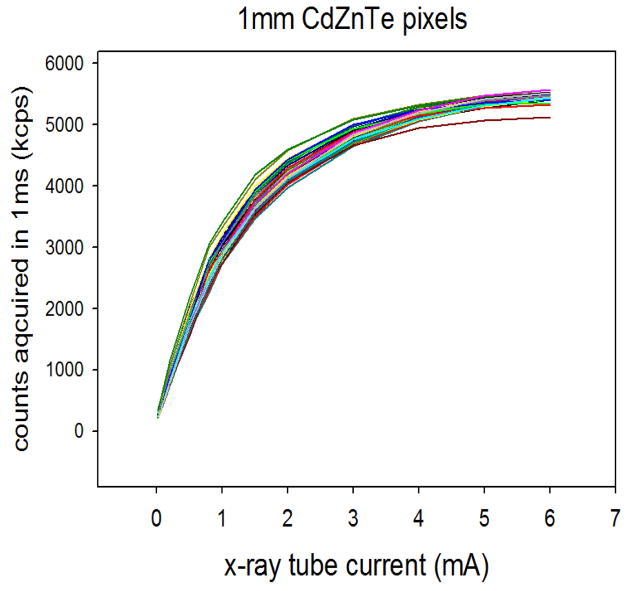
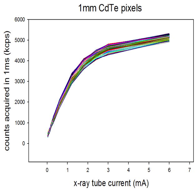
A CdZnTe sensor with 1 mm pixels was connected to an ASIC with a 20 ns peaking time. Measurements of the OCR as a function of input count rate (ICR) have been obtained. Figure 1 shows the OCR as a function of increasing ICR using CdZnTe with 1 mm pixels for a tube setting of 120 kVp at various tube currents and at a distance of about 20 cm from the tube’s focal spot and with a 1 mm Cu filter between the source and detector. A CdTe sensor with 1 mm pixels was connected to the same ASIC and measurements of the OCR as a function of ICR have been obtained under the same conditions. Figure 2 shows the OCR as a function of increasing ICR using CdTe with 1 mm pixels. In both cases data is acquired in a 1 ms frame time and represents thousands of counts per second (kcps) per pixel. For both the CdZnTe and CdTe the 1 mm pixels exhibit a linear OCR response to between 1.5 and 2 million counts per second (Mcps) per pixel using preamplifiers with 20 ns peaking time within the ASIC. Also for both materials the OCR saturates above 5 Mcps per pixel due to pulse pile-up.
Figure 1.
The output count rate (OCR) as a function of increasing X-ray tube current for an array of 1 mm CdZnTe pixels connected to a fast 20 ns peaking time parallel channel ASIC.
Figure 2.
The output count rate (OCR) as a function of increasing X-ray tube current for an array of 1 mm CdTe pixels connected to a fast 20 ns peaking time parallel channel ASIC.
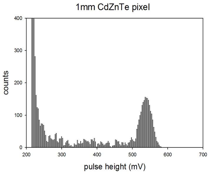
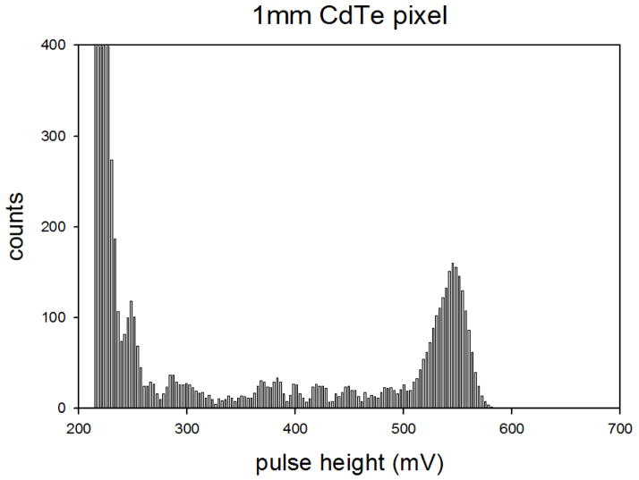
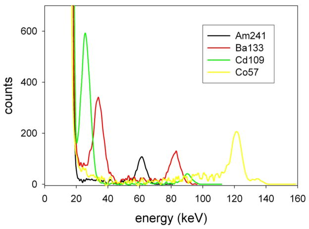
The CdZnTe and CdTe detectors with 1 mm pixels have also been used to obtain spectra from radionuclide sources. Figure 3 shows an 241Am spectrum taken with the CdZnTe sensor with 1 mm pixels. An approximately 10 μCu 241Am source was placed directly above the sensor on the cathode (incident) side and data was taken over several minutes. A single threshold for each pixel is swept from approximately 140 keV down to approximately 10 keV in 0.5 keV steps. The resulting plot of the number of counts above the threshold setting as a function of threshold setting is then passed through a smoothing filter and differentiated to produce the pulse height spectrum. An 241Am spectra from the CdTe sensor with 1 mm pixels has been obtained under the same conditions. Figure 4 shows the 241Am spectrum taken with the CdTe sensor with 1 mm pixels. In order to determine the noise floor and resolution in terms of energy the detector needs to be calibrated. This is done by sweeping all the thresholds in the presence of 109Cd, 133Ba, 241Am, and 57Co sources and differentiating the resulting curves to obtain spectra in terms of the pulse height response for the detector. Figure 5 shows spectra from all these sources where a linear calibration used from the corresponding peaks to convert from pulse height to energy demonstrating a noise floor of 20 keV. The photopeaks, from 22 keV to 135 keV, show a full width at half maximum (FWHM) of approximately 7 keV and is independent of energy indicating good charge collection across the entire dynamic range for CT.
Figure 3.
Pulse height spectra from a 241Am source taken with a typical pixel from an array of 1 mm CdZnTe pixels connected to a fast 20 ns peaking time parallel channel ASIC.
Figure 4.
Pulse height spectra from a 241Am source taken with a typical pixel from an array of 1 mm CdTe pixels connected to a fast 20 ns peaking time parallel channel ASIC.
Figure 5.
Energy spectra from 109Cd, 133Ba, 241Am, and 57Co sources taken with a typical pixel from an array of 1 mm CdTe pixels connected to a fast 20 ns peaking time parallel channel ASIC.
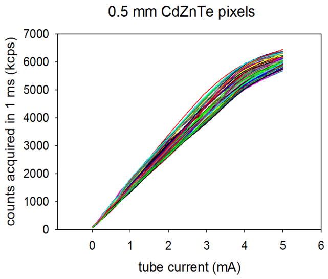
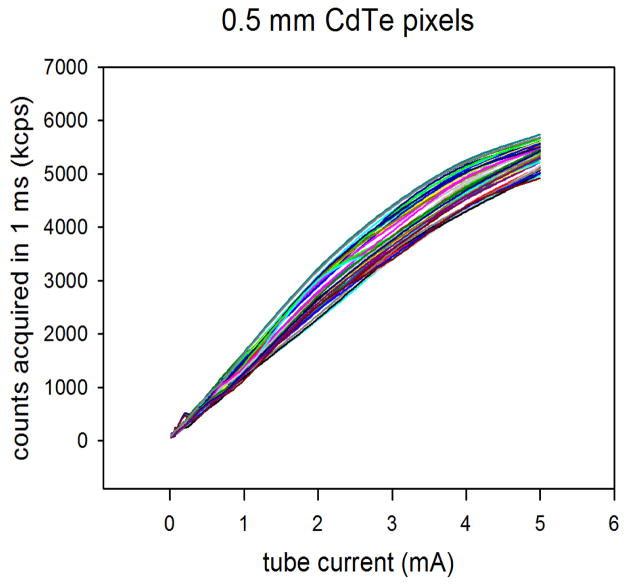
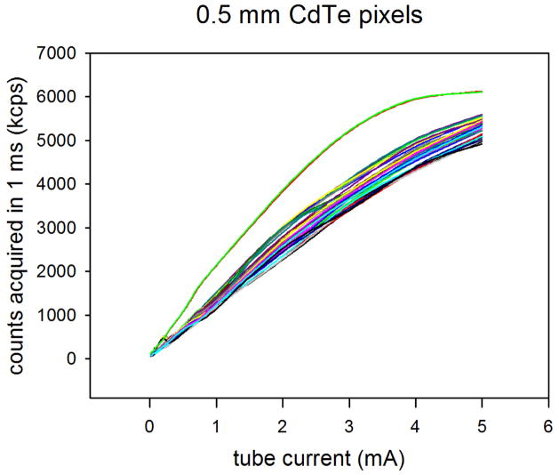
A CdZnTe sensor with 0.5 mm pixels was connected to an ASIC with a 10 ns peaking time. Measurements of the OCR as a function of input count rate (ICR) have been obtained. Figure 6 shows the OCR as a function of increasing ICR using CdZnTe with 0.5 mm pixels for a tube setting of 120 kVp at various tube currents and at a distance of about 10 cm from the tube’s focal spot with a 0.5 mm Cu filter between the source and detector. A CdTe sensor with 0.5 mm pixels was connected to the same ASIC and measurements of the OCR as a function of ICR have been obtained under the same conditions. Figure 7 shows the OCR as a function of increasing ICR using CdTe with 0.5 mm pixels. In both cases data is acquired in a 1 ms frame time and is in kcps per pixel. For both the CdZnTe and CdTe the 0.5 mm pixels exhibit a linear OCR response to between 3 and 4 million counts per second (Mcps) per pixel using preamplifiers with 10 ns peaking time within the ASIC. A 15% OCR deficit due to pulse pile-up occurs at about 5.5 Mcps per pixel for both materials.
Figure 6.
The output count rate (OCR) as a function of increasing X-ray tube current for an array of 0.5 mm CdZnTe pixels connected to a fast 10 ns peaking time parallel channel ASIC.
Figure 7.
The output count rate (OCR) as a function of increasing X-ray tube current for an array of 0.5 mm CdTe pixels connected to a fast 10 ns peaking time parallel channel ASIC.
The CdZnTe and CdTe sensors with 0.5 mm pixels have also been used to obtain spectra from radionuclide sources. Figure 8 shows an 241Am spectrum taken with the CdZnTe sensor with 0.5 mm pixels. An approximately 10 μCu 241Am source was placed directly above the sensor on the cathode (incident) side and data was taken over several minutes by sweeping thresholds across the dynamic range and differentiating the resulting curve as described previously. Charge sharing between nearest neighbor pixels resulting from characteristic x-rays of Cd and Te and other effectsis expected to increase as a function of decreasing pixel size. This will produce increased tailing (counts below the photopeak) in response to X-rays with energies above the k-edge of Cd, or Te. Notice there is increased tailing as compared to results obtained with 1 mm pixels (see figure 3 and 4) as expected from an increase in charge sharing effects. The FWHM energy resolution of the photopeak is approximately 7 keV similar to what was obtained with 1 mm pixels and a 20 ns peaking time. The CdTe sensor with 0.5 mm pixels was connected to the same ASIC and a measurement of the FWHM energy resolution has been obtained under the same conditions with essentially the same results as seen in Figure 8.
Figure 8.
Pulse height spectra from a 241Am source taken with a typical pixel from an array of 0.5 mm CdZnTe pixels. Similar results are obtained with 0.5 mm CdTe pixels.
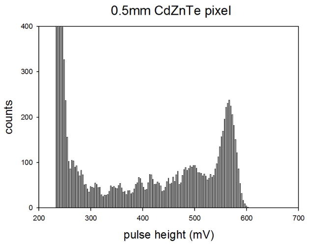
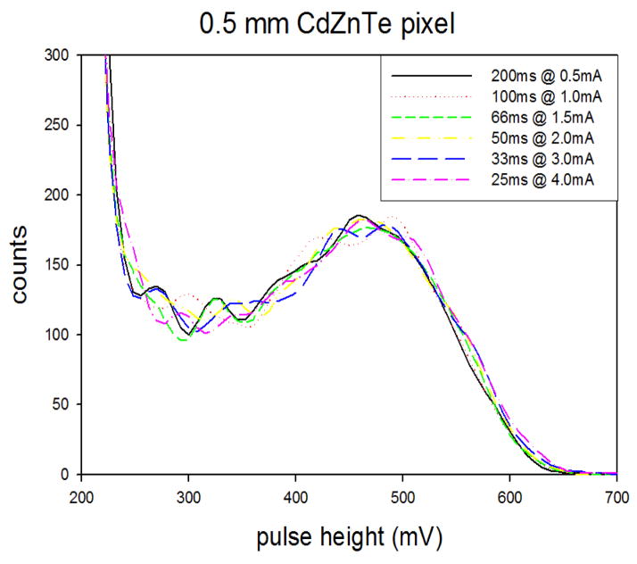
In order to demonstrate an energy response independent of flux, spectra has also been recorded by sweeping thresholds with an incident 140 kVp beam at increasing X-ray tube current. Figure 9 shows X-ray spectra recorded using a CdZnTe sensor with 0.5 mm pixels connected to a four thresold ASIC using a 10 ns peaking time where results from a typical single pixel as shown. The spectra in Figure 9 are normalized by plotting the number of counts divided by the tube current from an x-ray tube set to 80 kVp operated from 0.5 mA to 4.0 mA of tube current at approximately 10 cm for an incident flux of about 2.5 Mcps/mm2 (0.5 mA) to 20 Mcps/mm2 (4 mA). At a threshold value (pulse height) of 250 mV no counts are seen without x-rays or sources present. Below 250 mV counters fill with noise and reset when they overflow therefore no meaningful data can be obtained below a threshold value of 250 mV which corresponds to approximately 20 keV. The spectra up to 20 Mcps/mm2 OCR corresponding are essentially the same showing very little pile up. Pulse pile up or dead time losses eventually limit the upper bound on the flux linearity of the detector and read out. The high flux rate of this device extends the range for photon counting detectors as compared to previous devices of this type.
Figure 9.
Pulse height spectra from an X-ray tube with a 80 kVp setting taken with a typical pixel from an array of 0.5 mm CdZnTe pixels at various tube currents. Similar results are obtained with 0.5 mm CdTe pixels.
One of the CdTe sensors with 0.5 mm pixels contained a pair pairs of what we suspect are merged solder balls which connect two adjacent pixels to two adjacent ASIC inputs in parallel. Figure 10 shows the OCR as a function of increasing ICR using a CdTe sensor with 0.5mm pixels and suspected merged solder balls affecting two pixels taken under the same conditions as with all the 0.5 mm pitch detectors fabricated. It is expected that each of the two preamplifiers involved will count all the x-ray interactions producing charge occurring in both pixels but that the signal from each interaction will be divide between the two. Therefore the OCR should be twice the ICR in the linear portion of the OCR response curve and the pulse height for a radionuclide photopeak will be at half the voltage as compared to um-merged pixels. Figure 10 shows four pixels which are in two nearest neighbor pair which show twice the OCR as a function of ICR in the linear portion of the curves as compared to all other pixels. An 241Am spectra from one of the pixels suspected to be merged with a nearest neighbor pixel at the input taken under the same conditions as all previous 241Am spectra. The pulse heights for events in the photopeak are at about half the voltage for unmerged pixels as expected. An additional difference between merged pixels and unmerged pixels is that the capacitance on the input to both preamplifiers will be increase by a factor of two, Given that the peaking time is very fast the electronic noise is dominated by capacitance and we would expect degraded energy resolution for merged pixels which was the case with about twice the FWHM spread as compared to unmerged pixels. In order to avoid merged solder balls between the 05 mm pixels it is necessary to optimize the reflow procedures for high pixel yield.
Figure 10.
The output count rate (OCR) as a function of increasing X-ray tube current for another array of 0.5 mm CdTe pixels connected to a fast 10 ns peaking time parallel channel ASIC. In this device two nearest neighbor pixels are suspected of being interconnected.
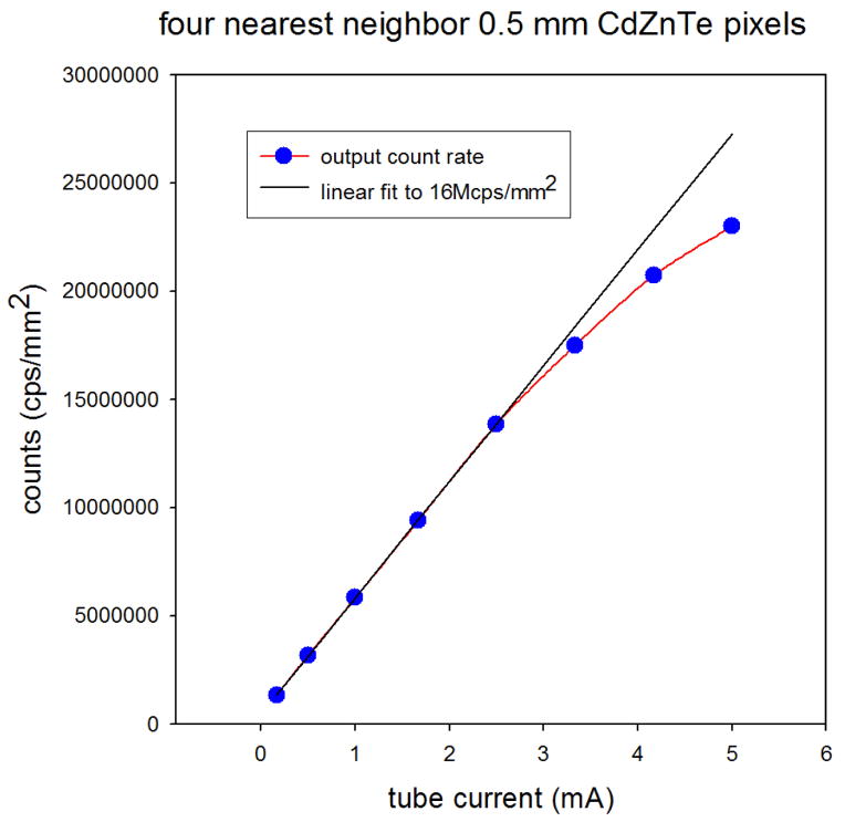
For applications in clinical CT, which requires an intrinsic spatial resolution of 1 mm, four nearest neighbor 0.5 mm pixels in a 1 mm2 block are summed with four global thresholds levels fixed to generate four energy windows during patient scanning. Since each of the four individual thresholds per pixel contains a DAC voltage adjustment, the offset and gain differences between channels can be compensated for at any energy within the dynamic range. For this reason there is no spectral distortion by summing the data from the four nearest neighbor pixels. Figure 11 shows the OCR and a function of ICR for a typical 1 mm2 block of 0.5 mm pixels from CdZnTe. All the counts above the threshold set to 30 keV is plotted. The OCR is linear to 16 Mcps/mm2.
Figure 11.
Output count rate (OCR) as a function of increasing x-ray tube current (ICR) from four nearest neighbor 0.5 mm by 0.5mm pitch pixels patterned on 3 mm thick CdZnTe and connected to a 2D ASIC with a 10 ns peaking time. Similar results are obtained with 0.5 mm CdTe pixels.
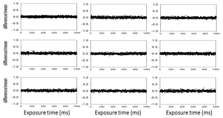
The temporal stability and uniformity under the high flux expected in CT and NDT applications has been measured using the CdZnTe and CdTe sensors with 0.5 mm pixels. One thousand temporally contiguous 1 ms frames are acquired with an average OCR of 3 Mcps per pixel which give approximately 3000 counts per frame per pixel. Nine typical pixels, where three pixels each are taken from the 0.5 mm pitch CdZnTe and CdTe sensors whose OCRs are show in figures 6, 7, and 10 respectively. Figure 12 shows the difference in the number of counts in an individual frame divided by the mean versus the mean. No drift is detected and additionally the variance versus the mean falls within the counting statistics of the mean.
Figure 12.
Graphs of the difference divided by the mean versus time as determined by acquiring data in 1000 successive 1 ms frame times from an ASIC with a 10 ns peaking time under constant flux from a clinical CT X-ray generator.
Conclusions
In this study, CdZnTe and CdTe sensors with 1 mm and 0.5 mm pixels have been fabricated and connected to fast energy dispersive single X-ray photon counting readout ASICs. Measurements of the OCR and FWHM energy resolution have been performed. The results are essentially equivalent in the performance we have achieved from geometrically identical CdZnTe and CdTe sensors. The OCR for sensors with 1 mm pixels connected to an ASIC using a 20 ns peaking time is shown to saturate above 5 Mcps/mm2 (see figure 1 and 2) with matching results. The OCR measurement is performed by recording all the counts above an individual threshold for each pixel set to 30 keV as a function of increasing X-ray tube current. The FWHM energy resolution for sensors with 1 mm pixels connected to an ASIC using a 20 ns peaking time is shown to be about 7 keV at 60 keV (see figure 3 and 4) with matching results. The FWHM measurement is made by sweeping an individual threshold for a single (typical) pixel from high to low energy and differentiating the data with respect to energy. A smoothing function is applied to the integrated spectra to reduce the amplification of statistical fluctuations in the digitally differentiated spectra. The OCR for sensors with 0.5 mm pixels connected to an ASIC using a 10 ns peaking time is shown to linear up to 16 Mcps/mm2 (see figure 6 and 7) with matching results. At 22 Mcps/mm2 an approximate 15% deviation from liniearity is observed in both materials. In this case the increased OCR is due to both the use of smaller pixels and a faster peaking time. The faster peaking time is demonstrated by the increased linearity of the OCR curves. The FWHM energy resolution for sensors with 0.5 mm pixels is shown to be about 7 keV at 60 keV (see figure 8) similar to the results obtained with 1 mm pixels (see figure 3 and 4), however, there is an increase in the number of counts below the photopeak due to charge sharing from k-escape. The energy response has also been investigated by generating spectra from an X-ray generator with a voltage setting of 80 kVp and increasing flux from 2.5 Mcps/mm2 to 20 Mcps/mm2 showing flux independent results. This work demonstrates that both CdZnTe and CdTe room temperature sensors connected to ASICs show promise as high flux energy dispersive photon counting room temperature detectors for use in X-ray imaging applications such as CT.
Conventional (single energy) x-ray multi-slice CT scanners using energy integrating current mode detectors provide three-dimensional gray-scale images that accurately delineate organs and tissues and help physicians make accurate diagnoses. However, there are major limitations in single energy CT technologies, namely that gray-scale images are not tissue-type specific, contrasts between different tissues are not sufficient, and large doses of radiation to patients are necessaryxxviii. Our energy resolved counting mode CT detectors overcome the major limitations in conventional CT technologies involving large doses of radiation to patients, insufficient contrast resolution to discriminate tissues, and a lack of material decomposition methods for NDT. Dual-kVp (dual energy) x-ray multi-slice CT scanners have been developed using current mode detectors to reduce dose and increase material specific contrast. However there are limitations in use of these systems primarily due to the excessive cost of a system requiring two rows of detectors and or two x-ray tubes for dual energy scanning. Our counting mode CT detectors overcome the major limitations in the clinical use of dual energy CT technologies involving the cost of dual-kVp systems by acquiring energy resolved data in a single scan with a single x-ray tube using existing conventional CT sources and gantries. Recently, k-edge (triple energy) CT has been proposed as a potential method for functional CT wherein heavy metal nanoparticles are used as targeted imaging agents (high-Z imaging biomarkers)xxix. K-edge CT imaging combined with targeted biomarkers could provide simultaneous functional and anatomical tomographic images in a single scan thus providing a new quantitative molecular imaging platform enabling small tumor mass and size quantification for early cancer diagnosis and accurate prognosis. K-edge CT imaging requires triple-energy scanning. Triple-energy imaging could be implemented in a triple-kVp system however the cost and complexity of such a system make its development impractical. Our photon counting CT detectors as developed in this project will create the only CT system in the world capable of performing clinical k-edge CT. For these reasons our counting mode CT detectors are expected to have a significant impact on medical CT in both the clinic (single and dual energy) as well as in the development of new functional methods (triple energy). The ability to perform multiple basis material decomposition (up to the number of energy bins per pixel) extends the use of CT for NDT.
Acknowledgments
This work is supported in part by the following grants from the National Institute of Biomedical Imaging and Bioengineering: R44EB008612; R44EB012379.
Footnotes
Publisher's Disclaimer: This is a PDF file of an unedited manuscript that has been accepted for publication. As a service to our customers we are providing this early version of the manuscript. The manuscript will undergo copyediting, typesetting, and review of the resulting proof before it is published in its final citable form. Please note that during the production process errors may be discovered which could affect the content, and all legal disclaimers that apply to the journal pertain.
References
- i.Cammin J, Srivastava S, Barber WC, Iwanczyk JS, Hartsough NE, Nygard E, Wessel JC, Malakhov N, Taguchi K. A tabletop clinical x-ray CT scanner with energy-resolving photon counting detectors. presented at the Medical Imaging 2011: Physics of Medical Imaging; Lake Buena Vista, Florida, USA. 2011. pp. 79611S–79611S–7. [Google Scholar]
- ii.Taguchi K, Zhang M, Frey EC, Wang X, Iwanczyk JS, Nygard E, Hartsough NE, Tsui BMW, Barber WC. Modeling the performance of a photon counting x-ray detector for CT: Energy response and pulse pileup effects. Medical Physics. 2011;38:1089–1102. doi: 10.1118/1.3539602. [DOI] [PMC free article] [PubMed] [Google Scholar]
- iii.Le HQ, Molloi S. Segmentation and quantification of materials with energy discriminating computed tomography: A phantom study. Med Phys. 2011;38:228–237. doi: 10.1118/1.3525835. [DOI] [PMC free article] [PubMed] [Google Scholar]
- iv.Tomita Y, Shirayanagi Y, Matsui S, Misawa M, Takahashi H, Aoki T, Hatanaka Y. X-ray color scanner with multiple energy differentiate capability. IEEE Nucl Sci Symp Conf Rec. 2004;6:3733–3737. [Google Scholar]
- v.Llopart X, Campbell M, Dinapoli R, San Segundo D, Pernigotti E. Medipix2: A 64-k pixel readout chip with 55-μm square elements working in single photon counting mode. IEEE Trans Nucl Sci. 2002;49(5):2279–2283. [Google Scholar]
- vi.Johns PC, Dubeau J, Gobbi DG, Li M, Dixit S. Photon-Counting Detectors for Digital Radiography and X-Ray Computed Tomography. SPIE. 2002;TD01:367–369. [Google Scholar]
- vii.Shikhaliev PM, Tong X, Molloi S. Photon computed tomography: Concept and initial results. Med Phys. 2005;32(2):427–436. doi: 10.1118/1.1854779. [DOI] [PubMed] [Google Scholar]
- viii.Maidment A, Ullberg C, Lindman K, Adelow L, Egerstrom J, Eklund M, Francke T, Jordung U, Kristoffersson T, Lindqvist L, Marchal D, Olla H, Penton E, Rantanen J, Solokov S, Weber N, Westerberg H. Evaluation of a photon-counting breast tomosynthesis imaging system. Medical Imaging 2005, Proceedings of the SPIE; 2005. pp. 572–582. [Google Scholar]
- ix.Chmeissani M, Frojdh C. First Experimental Tests with a CdTe Photon Counting Pixel Detector Hybridized with a Medipix2 Readout Chip. IEEE Trans Nucl Sci. 2004;51(5):2379–2385. [Google Scholar]
- x.Bisogni M, Gambaccini M. A digital system based on a bi-chromatic X ray source and a single photon counting device: a single exposure dual energy mammography approach. Proc SPIE. 2002;4682:620–632. [Google Scholar]
- xi.Mikulec B, Campbell M, Heijne E, Llopart X, Tlustos L. X-ray Imaging Using Single Photon Processing with Semiconductor Pixel Detectors. NIM, A. 2003;511:282–286. [Google Scholar]
- xii.Iwanczyk JS, Nygard E, Meirav O, Arenson J, Barber WC, Hartsough NE, Malakhov N, WJC Photon counting energy disparsive detector arrays for x-ray imaging. Transactions on Nuclear Science. 2009;56(3):1820. doi: 10.1109/TNS.2009.2013709. [DOI] [PMC free article] [PubMed] [Google Scholar]
- xiii.Barber WC, Malakhov N, Damron MQ, Hartsough NE, Moraes D, Weilhammer P, Nygard E, Iwanczyk JS. Guard ring elimination in CdTe and CdZnTe detectors. IEEE Nucl. Sci. Symp. Conference Record; 2006. pp. 2414–2416. [Google Scholar]
- xiv.Barber WC, Iwata K, Hasegawa BH, Bennett PR, Cirignano LJ, Shah KS. Current mode operation of a CdZnTe for CT imaging. Penetrating Radiation Systems and Applications IV, SPIE. 2002;4786:144–150. [Google Scholar]
- xv.Taguchi K, Frey EC, Wang X, Iwanczyk JS, Barber WC. An analytical model of the effects of pulse pileup on the energy spectrum recorded by energy resolved photon counting x-ray detectors. Med Phys. 2010;37(8):3957–3969. doi: 10.1118/1.3429056. [DOI] [PMC free article] [PubMed] [Google Scholar]
- xvi.Leng S, Yu L, Wang J, Fletcher JG, Mistretta CA, McCollough CH. Noise reduction in spectral CT: Reducing dose and breaking the trade-off between image noise and energy bin selection. Med Phys. 2011;38:4946–4957. doi: 10.1118/1.3609097. [DOI] [PubMed] [Google Scholar]
- xvii.Tapiovaara MJ, Wagner R. SNR and DQE analysis of broad spectrum X-ray imaging. Physics in Medicine and Biology. 1985;30(6):519–29. [Google Scholar]
- xviii.Shikhaliev PM. Beam hardening artefacts in computed tomography with photon counting, charge integrating and energy weighting detectors: a simulation study. Physics in Medicine and Biology. 2005;50(24):5813–27. doi: 10.1088/0031-9155/50/24/004. [DOI] [PubMed] [Google Scholar]
- xix.Hu H, He HD, Foley WD, Fox SH. Four multidetector-row helical CT: image quality and volume coverage speed. Radiology. 2000 Apr;215(1):55–62. doi: 10.1148/radiology.215.1.r00ap3755. [DOI] [PubMed] [Google Scholar]
- xx.Bennett PR, Shah KS, Cirignano LJ, Klugerman LP, Moy LP, Squillante MR. Characterization of polycrystalline TlBr films for radiographic detectors. IEEE Trans Nucl Sci. 1999;46:266–270. [Google Scholar]
- xxi.Shah KS, Bennett P, Dimitriyev Y, Cirignanno L, Klugerman M, Squillante MR, Street RA, Rahn JT, Ready SE. PbI2 for high resolution digital x-ray imaging. Proceedings of the SPIE. 1999;3770:164–173. [Google Scholar]
- xxii.Street RA, Rahn JT, Ready SE, Shah K, Bennett PR, Dimitriyev Y, Mei P, Lu JP, Apte RB, Ho J, Schylenbergh K, Lemmi F, Braiman M, Nylen P. X-ray imaging using lead iodide as a semiconductor detector. Proceedings of the SPIE. 1999;3659:36–47. [Google Scholar]
- xxiii.Schieber M, Hermon H, Zuck A, Vilensky A, Melekhov L, Shatunovsky R, Meerson E, Saado H. Polycrystalline mercuric iodide detectors. Proceedings of the SPIE. 1999;3770:146–155. [Google Scholar]
- xxiv.Schieber M, Zuck A, Melekhov L, Shatunovsky R, Hermon H, Turchetta R. High flux x-ray response of composite mercuric iodide detectors. Proceedings of the SPIE. 1999;3768:296–309. [Google Scholar]
- xxv.Knoll GF. Radiation Detection and Measurement. Wiley; New York: 1989. pp. 337–386.pp. 584–651. [Google Scholar]
- xxvi.Patt BE, Iwanczyk JS, Vilkelis G, Wang YJ. New Gamma-ray Detector Structures for Electron Only Charge Carrier Collection Utilizing High-Z Compound Semiconductors. Nucl Instr & Meth in Phys Res. 1996;A380:276–281. [Google Scholar]
- xxvii.Squillante MR, Shah KS. Other materials: Status and Prospects, Chapter 12, Semiconductors for Room Temperature Nuclear Detector Applications. 1995;43:465. [Google Scholar]
- xxviii.Mettler FJ. CT scanning: patterns of use and dose. J Radiol Prot. 2000 Dec;20(4):353–9. doi: 10.1088/0952-4746/20/4/301. [DOI] [PubMed] [Google Scholar]
- xxix.Schlomka JP, Roessl E, Dorscheid R, Dill S, Martens G, Istel T, Bäumer C, Herrmann C, Steadman R, Zeitler G, Livne A, Proksa R. Experimental feasibility of multi-energy photon-counting K-edge imaging in pre-clinical computed tomography. Phys Med Biol. 2008;53:4031–4047. doi: 10.1088/0031-9155/53/15/002. [DOI] [PubMed] [Google Scholar]


