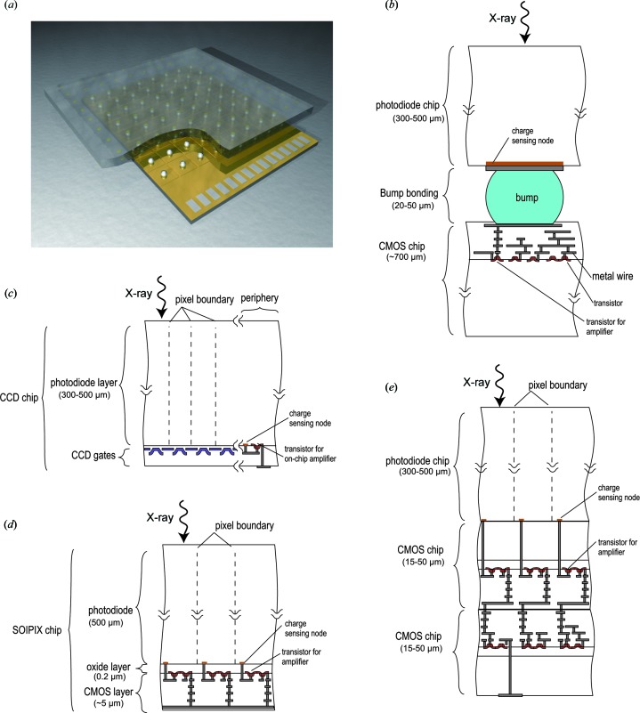
Figure 1.
(a) Schematic layout of a hybrid detector. The top layer is the pixelated sensor, where the impinging X-ray photons are absorbed and their energy transferred into an electrical signal. Each pixel of the sensor is connected to a pixel of the readout chip, where the signal is further processed and transmitted to the backend electronics. (b) A cross-sectional view of a hybrid-detector pixel. The sensor, with a photodiode, and the readout chip are connected by a bump. The signal charge generated in the photodiode flows to the charge-sensing node and spreads over the bump and the transistor through metal wires, which have a large total capacitance. The resulting signal voltage is low and it is amplified by circuitry composed of transistors (red) in the readout chip. Because the photodiode and CMOS readout chips are fabricated separately, they can be optimized independently. (c) In contrast, charge-coupled device (CCD) detectors are made of a single chip. The pixel has a gate structure without transistors, which makes smaller pixels possible. The signal charge generated at the photodiode is transferred to the periphery of the sensor, where the charge-sensing node (orange) is located. The charge-sensing node is connected to the transistor (red). Because the charge is spread over a confined space, the associated capacitance is low and the resulting signal voltage becomes higher than that for a hybrid detector. Owing to this conversion scheme with a low input capacitance, noise performance as low as a few electrons is possible (see §4.1.1). (d) In SOI pixel technology (§4.2.1), the transistor for the amplifier is located inside the pixel, while the charge-sensing node and transistor are very close (less than 1 µm). The associated input capacitance is thus kept low, enabling better noise performance. However, the chip is made from a single SOI wafer, so optimization of the photodiode and CMOS transistor should be done in one production recipe. (e) For the VIPIC detector as an example of the three-dimensional integration case (§4.2.4), the charge-sensing node is located close enough to the amplifier transistor to provide a chance of realising low-noise performance. In addition, the photodiode and two CMOS chips can be optimized separately, giving considerable freedom in design and production. Thicknesses shown in this figure are ones for possible implementation and are provided here to give the reader an idea of physical size.

