Abstract
The deformation of monolayer graphene, produced by chemical vapor deposition (CVD), on a polyester film substrate has been investigated through the use of Raman spectroscopy. It has been found that the microstructure of the CVD graphene consists of a hexagonal array of islands of flat monolayer graphene separated by wrinkled material. During deformation, it was found that the rate of shift of the Raman 2D band wavenumber per unit strain was less than 25% of that of flat flakes of mechanically exfoliated graphene, whereas the rate of band broadening per unit strain was about 75% of that of the exfoliated material. This unusual deformation behavior has been modeled in terms of mechanically isolated graphene islands separated by the graphene wrinkles, with the strain distribution in each graphene island determined using shear lag analysis. The effect of the size and position of the Raman laser beam spot has also been incorporated in the model. The predictions fit well with the behavior observed experimentally for the Raman band shifts and broadening of the wrinkled CVD graphene. The effect of wrinkles upon the efficiency of graphene to reinforce nanocomposites is also discussed.
Keywords: CVD graphene, wrinkles, deformation mechanics, Raman spectroscopy
Following its first isolation in 2004, graphene has shown huge potential in both fundamental studies1 and industrial applications.2 Currently, one of the urgent targets is to grow large-size, continuous, and defect-free graphene. The chemical vapor deposition method (CVD) opens a route to achieve these targets at low cost.3 However, the grain boundaries formed after the graphene grains become stitched together4 affect its performance,5−7 for example, in applications such as transparent electrodes, since these boundaries impede electrical transport.4,8 Moreover, CVD-grown graphene typically has to be transferred to other substrates for use,9,10 during which wrinkles can be induced10,11 as a result of the different thermal expansion of the substrates,12,13 the replication of the substrate topography,14 and the transfer process itself.9 These wrinkles have been observed on graphene-based transparent electrodes15,16 and are thought to further alter its mechanical stretchability,17 electronic structure,18 and local potential.19 It is also thought that the presence of wrinkles can affect the deformation of graphene in shear,20 the deformation of graphene oxide paper,21 and the ability of graphene oxide to reinforce polymer matrices in nanocomposites.22 Although wrinkling appears to be an inherent property of graphene due to its extremely low bending rigidity23 even when it is fully embedded into polymer matrices,24 there has as yet been no systematic experimental study of its effect upon the mechanical response of graphene.
Raman spectroscopy is a versatile tool to study graphene;25−27 in particular, it can be useful in the study of number of layers,25,28 stacking order,28,29 and doping, etc.30,31 It has also been used to monitor the deformation of graphene32 and to demonstrate that continuum mechanics is still valid even for a one-atom thick material.24,33−35 In many of the previous studies on large flat graphene flakes, it was possible to assume uniformity of the graphene within the spatial resolution of the Raman laser spot (around 1–2 μm in diameter). However, when the graphene is <1 μm in size or at edges, Raman spectroscopy only provides limited information as a result of nonuniformity of the Raman scattering due to the structural nonuniformity of the graphene and also the spatial variation of the excitation intensity over the laser spot.36,37 In fact, when difficulties are encountered in this situation, it is usually assumed that the signal detected is the average Raman scattering emanating from all of the graphene within the spot.24,37,38
In this work, Raman spectroscopy has been employed to monitor the deformation mechanics of monolayer CVD graphene on a poly(ethylene terephthalate) substrate (CVD graphene/PET) where the PET film is flat but the graphene is wrinkled. It is found that upon deformation of the film the shift of the graphene Raman 2D band with strain and the band broadening characteristics are quite different from that observed for mechanically exfoliated monolayer graphene flakes. It is shown that the wrinkles have the effect of separating the graphene mechanically into isolated islands, with each island being similar in size to the Raman laser spot. It is demonstrated that inside each island the stress will be transferred nonuniformly from the PET to the graphene, and this allows the unusual Raman band shift and broadening behavior to be explained. The effect of such wrinkles upon the ability of graphene to reinforce nanocomposites will also be discussed below.
Results and Discussion
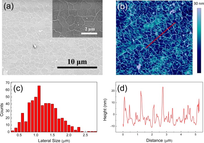
The scanning electron microscope (SEM) images in Figure 1a of the surface of the CVD graphene/PET show the network of CVD graphene islands separated by wrinkles with a height of around 20 nm, as revealed by atomic force microscopy (AFM) (Figure 1b and d).
Figure 1.
(a) SEM and (b) AFM images of the CVD graphene. (c) Distribution of the lateral dimensions of the graphene islands. (d) AFM height profile of the inset red line in (b) showing the height of the wrinkles.
The wrinkled graphene microstructure resembles those found previously.39,40 It is thought that the wrinkles form in the CVD graphene for at least two reasons. First, it appears that the Cu substrate employed is never completely flat. Second, they will form as a result of the different thermal coefficients of Cu substrate (∼20 × 10–6 K–1)41 and graphene (−8.0 × 10⁻⁶ K–1).42 After growth, when the CVD graphene cools from a typical growth temperature of 1000 °C, the Cu contracts but the graphene expands, resulting in a compressive strain of 2–3% in the graphene.14 This is at least 1 order of magnitude higher than the critical strain required for graphene buckling.24,43 Such high strains can induce severe high order buckling deformation which does not relax back when the strain is released and gives rise to a network of large out-of-plane wrinkles or folds, in good agreement with computational simulations.18 It also bears a strong similarity to the wrinkled microstructure found for thin films of copper on layered-crystal surfaces, again formed through a mismatch in thermal expansion coefficients.13
The wrinkles separate the graphene surface into small isolated islands with their size distribution, based upon more than 500 measurements as detailed in the Supporting Information, shown in Figure 1c. It can be seen that there is a broad distribution of the lateral dimensions of the islands, with a mean value around 1.2 μm but also with some larger islands of up to 3 μm in diameter.
Raman spectroscopy has been employed to monitor interfacial stress transfer from the PET substrate to the CVD graphene, and the whole CVD graphene/PET film has been modeled as a nanocomposite structure.22,33,44 The Raman spectra of the PET substrate and the CVD graphene/PET are shown in Figure 2. The 2D band at around 2700 cm–1 (also known as the G′ band) results from two phonons near the K point.25 The graphene G band overlaps partially with the PET band (Figure 2), and so only the 2D band has been used here for the analysis of stress transfer. The lack of a visible D band suggests the absence of defects (grain boundaries, etc.) even at the wrinkles.4 An estimate of the intensity ratio of the 2D band to the G band (after deconvolution from the strong adjacent PET band), along with a sharp 2D band with a full width at half-maximum around 30 cm–1, demonstrates that the CVD graphene is essentially a monolayer.25,45
Figure 2.
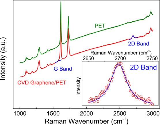
Raman spectra of the CVD graphene/PET and neat PET substrate. The background scattering was not removed from the spectra. Inset shows the experimental data (red circle) and the Lorentzian fitting (blue line) for the 2D band.
The initial position of the 2D band of the CVD graphene on the PET film of 2696.0 ± 2.2 cm–1 compared with the stress-free value of ∼2677 cm–1 from mechanically exfoliated monolayer graphene with 514 nm laser excitation46 clearly indicates that graphene on the substrate is in compression. It appears that the graphene islands are able to support the compressive loads, and it is only at the island boundaries that the compressive load is relieved by wrinkling.
The CVD graphene/PET was subjected to tensile deformation, and the shift of the graphene Raman 2D band, fitted with a Lorentzian function, was monitored to elucidate the deformation mechanics.47−49 When the specimen was strained uniaxially in tension the 2D band position (ω2D) downshifted with strain ε at a rate dω2D/dε = −12.8 ± 2.0 cm–1/%. At the same time, the 2D band broadened with strain and its full width at half-maximum (FWHM2D) increased approximately linearly with ε at a rate of dFWHM2D/dε = 9.3 ± 3.1 cm–1/% (Figure 3). The absence of discontinuities in the data in Figure 3 implies that the interface between the CVD graphene and the PET film remains intact up to a strain of at least 0.4%.50 The data shown in Figure 3 are determined from separate sets of measurements from 8 regions chosen a random the CVD graphene/PET as shown in the Supporting Information. The data points in Figure 3 were averaged from the eight sets of measurements at each strain level, and the standard deviations given above are determined from the slopes of the individual sets of measurements in the Supporting Information. The scatter in the data is a reflection of the variation in size of the individual graphene islands as shown in Figure 1c.
Figure 3.
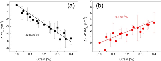
Variation of (a) ω2D and (b) FWHM2D under uniaxial strain. The solid lines are linear fits for both sets of data (mean values of eight sets of measurements).
Generally tensile strain induces phonon softening in graphene,48 which can be estimated using the knowledge of the Grüneisen parameter.51−53 For an ideal flat monolayer of graphene under uniaxial strain,52 the reference 2D band shift rate (dω2D/dε)ref is given as
| 1 |
where ω2D0 is the ω2D at zero strain, γ2D is the Grüneisen parameter for 2D band, and ν is the Poisson’s ratio of the substrate. As reported recently,54 the value of (dω2D/dε)ref is dependent on the laser excitation and the Poisson ratio of the matrix. In this study, if γ2D =3.55 and v = 0.35 is taken for PET,52 the value of (dω2D/dε)ref is estimated to be around −60 cm–1/% for flat monolayer on PET substrate. Additionally, the reference 2D band broadening rate with ε ((dFWHM2D/dε)ref) is found experimentally to be ∼12 cm–1/% using the 514 nm laser excitation.48 That is to say, when the monolayer graphene on PET substrate is fully stretched to a strain of 1%, ω2D downshifts by 60 cm–1 while at the same time FWHM2D increases by 12 cm–1. Hence, in the present study (Figure 3), the measured value of 2D band shift dω2D/dε is less than 25% of (dω2D/dε)ref, while the broadening rate dFWHM2D/dε is nearly 75% of that of (dFWHM2D/dε)ref.34,52,55 Such anomalous behavior is not found during the deformation of flat mechanically exfoliated monolayer graphene on PET,56 but wrinkles are invariably found when CVD graphene is transferred to a polymer substrate.10,57 In a previous study,58 we measured a band shift rate dω2D/dε of around −30 cm–1/% strain for CVD graphene deformed on a poly(methyl methacrylate) substrate, in which there were fewer wrinkles present than in the material employed in this present study.
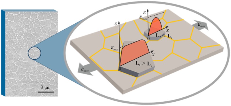
It will now be demonstrated that the low band shift rate dω2D/dε and higher-than-expected rate of broadening dFWHM2D/dε during deformation are both the result of the CVD graphene monolayer being wrinkled. In order to model this deformation behavior, it has been assumed that the microstructure of the graphene consists of a series of graphene islands bonded to the PET substrate, averaging 1.2 μm in diameter, separated by wrinkles that do not allow the transfer of stress between the isolated islands as shown in Figure 4a. Hence, in each individual island the axial strain will build up from zero at the wrinkles to become a maximum in the middle of the island. The exact form of the strain distribution will depend upon the size of the island and the efficiency of stress transfer from the underlying PET substrate. Figure S2 (Supporting Information) shows schematically how it is envisaged that the presence of the wrinkles leads to the graphene islands being isolated mechanically.
Figure 4.
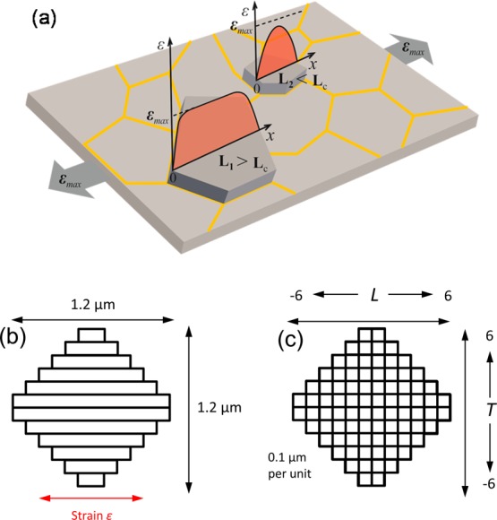
Schematic diagram (a) explaining the proposed stress transfer mechanism (Li is the length of the i-crystallite and Lc the critical transfer length) and showing (b) the strips in the graphene islands and (c) the corresponding elementary units.
It is then assumed that the ∼1.2 μm diameter graphene islands can be modeled as 12 strips of ∼0.1 μm wide mechanically independent graphene nanoribbons lying parallel to the direction of tensile stress (Figure 4b). Furthermore, it is assumed that the strain distributions in each nanoribbon can be estimated using “shear-lag theory” as has been done earlier for exfoliated graphene flakes subjected to deformation on a polymer substrate.33,59 Because of the comparable size of the graphene island to the Raman laser spot, it is also necessary to consider the effect of laser spot size in the analysis.36 It is shown in the Supporting Information that the effective size of the laser spot is of the order of 1.4 μm, i.e., similar to that of the graphene islands. Moreover, there is a variation of intensity across the spot (Gaussian distribution) as shown in the Supporting Information.60 Considering the size of the wrinkles, it is reasonable to assume that most of the laser spot intensity (∼90%) is within the graphene islands. Hence in order to calculate the spatial distribution of local strain and laser beam intensity, each strip is further divided into ∼0.1 μm square elementary units with their coordinates given by the longitudinal (L) and transverse (T) position parameters, where (−6 ≤ L ≤ 6) and (−6 ≤ T ≤ 6) (Figure 4c).
We now consider how stress transfer takes place from the PET substrate to graphene nanoribbon. It was shown using shear-lag theory59,61 that for an exfoliated monolayer graphene flake deformed on a polymer substrate the strain in the graphene should be zero near the edges and increase toward the center of the flake such that33
 |
2 |
where
| 3 |
and where εm is the matrix strain and εr is the real strain of graphene as a function of longitudinal position x along the stress direction. In this case, l is the length of the graphene nanoribbon along the stress direction, and s (= l/tg) is defined as the nanoribbon aspect ratio. Gm and Eg are the shear modulus of the matrix and the Young’s modulus of graphene, respectively, and tg and tm are the thickness of graphene and the elementary matrix, respectively. The parameter ns is generally accepted to be a measure of stress transfer efficiency, being higher for better stress transfer efficiency, and also increasing proportionally with the size of the monolayer graphene flake or nanoribbon.33 This theory implies a nonuniform strain in the graphene nanoribbons (and therefore the graphene islands) along the direction of axial stress, particularly when the nanoribbon is smaller than the “critical length”33 (twice of the distance it needs for strain to increase to the plateau value). This model of graphene islands isolated mechanically by wrinkles is analogous to the case of short fiber reinforcement in composites where there is no stress transfer across the fiber ends.62
The value of ns is proportional to the length of the graphene nanoribbon l (since s ∝ l); thus, both ns and l should be the function of the transverse position parameter T (Figure 4c), i.e., (ns)T and lT. Typically, the value of ns is taken to be of the order of 2 for a graphene nanoribbon 1.2 μm (T = ± 1) along the stress direction.33 It may also vary with the efficiency of stress transfer between the substrate and graphene as will be discussed later. Due to the symmetry of the strain and laser spot intensity distributions, only the units with positions (1 ≤ L ≤ 6, 1 ≤ T ≤ 6) have been considered here, and the distance between each unit (Figure 4c) is calculated through the unit center (i.e., the distance of unit (5,0) to the middle of island is calculated as (0.1 × 5) – 0.05 = 0.45 μm). On this basis, eq 2 can be modified to determine the strain in each individual unit εr(L,T) in Figure 4c as
 |
4 |
Figure 5a shows the predicted strain distribution within a ∼1.2 μm diameter graphene island for a PET substrate strain of 0.4%. It can be seen that the strain is zero at the edges of the island and increases to a maximum of only 0.14% in the center of the island. This demonstrates clearly that the presence of the wrinkles reduces the efficiency of stress transfer to the graphene monolayer. In order to simulate the effect of deformation of the CVD graphene/PET upon the shift of the graphene 2D Raman band, however, both the nonuniform strain in the islands and any local variation in laser spot intensity have been taken into account. Figure 5b schematically shows the intensity distribution within a real circular laser spot calculated using Figure S5 and eq S3 (Supporting Information).
Figure 5.
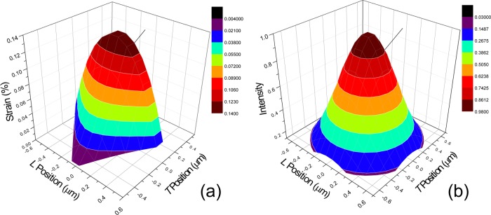
(a) Strain distribution in one island and (b) intensity distribution in the laser spot.
The 2D Raman band intensity collected from a unit (L,T) (Figure 4c) may be represented in the form of a Lorentzian function I(ω,L,T)63
| 5 |
where ωL,T is the position of the simulated band and FWHM is its full width at half-maximum. As constant band intensity persists even though the band position shifts so the maximum band intensity at ωL,T is normalized to be unity by a factor of FWHM/2, without affecting its other band parameters. Combining eqs 4 and 5 and eq S3 (Supporting Information), the normalized intensity distribution for the 2D Raman band under strain for each unit (L,T) in the graphene island may be given as eq 6.
 |
6 |
This equation takes into account both the local strain in the unit and the local intensity of the laser spot. The 2D Raman band collected in the whole island Itotal(ω) can then be determined as the summation of the constribution of all the elementary units (L,T) in the island:
| 7 |
For strain-free graphene, all the ωL,T are taken as zero for simplicity, and FWHM2D is taken as the average value for a graphene monolayer flake of 27 cm–1.28,64 The ideal values from exfoliated flat graphene flakes of (dω2D/dε)ref = −60 cm–1/% (eq 1) and (dFWHM2D/dε)ref = 12 cm–1/% can be used for 514 nm laser excitation, assuming a perfect interfacial adhesion within the graphene island.34 As mentioned previously, a typical value of ns = 2 is used for a monolayer graphene of length 1.2 μm along the stress direction. The Raman 2D band for whole graphene island calculated using eq 7 is shown in Figure 6.
Figure 6.
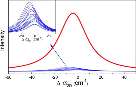
Simulated shift of Raman 2D band for each unit (1 ≤ L ≤ 6, 1 ≤ T ≤ 6, blue curves) and the integrated 2D band for the whole graphene island (red curve).
Consequently, the unusual band shift and broadening behavior of the wrinkled graphene can be determined from the summation of the Raman scattering from the different elementary units under strain. The lower rate of band shift per unit strain is the result of the small size of the graphene islands limiting the maximum strain and the nonuniform strain distribution causing more band broadening than would otherwise be expected. These effects are not found in larger flat mechanically exfoliated graphene flakes since the strain in them is reasonably uniform, except at the edges.33,47,48
In reality, the value of ns will vary depending upon the quality of interfacial stress transfer. With poor interfacial stress transfer, the ns value will be lower, leading to a less strained graphene island and a lower maximum strain at the island center. This less-strained graphene also results in different values of measured dω2D/dε and dFWHM2D/dε. In this case, the variation of ω2D and FWHM2D is predicted on the basis of eqs 6 and 7 using sets of ns values corresponding to different levels of interfacial adhesion (Figure 7). It can be seen that both sets of experimental data fall close to the line for ns = 2 and 3, demonstrating that the stress transfer between the PET and the CVD graphene within the graphene island is fairly good and comparable to the interface between exfoliated graphene and SU8/poly(methyl methacrylate).33
Figure 7.
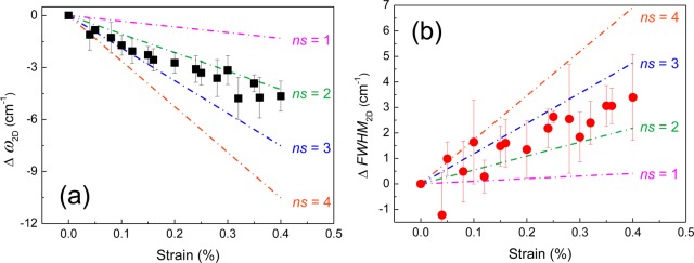
Predicted variation of (a) ω2D (b) FWHM2D as the function of strain for different ns values (used in eq 6 (colored lines). The data points are the experimental results from Figure 3.
The data in Figure 7 have been modeled assuming that the graphene islands and laser spots are approximately concentric. In reality, the Raman laser spot could be centered at any position relative to the graphene islands, either at their center, on their edges (Figure S6, Supporting Information) or at any intermediate position. This behavior has been modeled in the Supporting Information. The variation of ω2D and FWHM2D with strain for either the laser beam centered in the middle of the graphene island or at the edges have been calculated (Figure S7, Supporting Information), again using ns values of 2 and 3. It can be seen in the Supporting Information that the predicted variations of ω2D and FWHM2D with strain vary significantly with the position of the laser spot. Nevertheless, it is possible to fit the simulated lines to the experimental data by choosing appropriate ns values for any laser spot position. The fact that both the band shift and band broadening data can be fitted using the same value of ns gives confidence in the validity of the model.
Finally, it is worth considering the effect of wrinkles upon the ability of graphene to reinforce nanocomposites. To a first approximation, the effective Young’s modulus of the graphene scales with the Raman band shift rate per unit strain.22,65 Hence, the band shift rate of the wrinkled graphene, being less than 25% of that of flat mechanically exfoliated material, implies that it will have an effective Young’s modulus of only around 250 GPa, as opposed to ∼1TPa for flat graphene.66 In this present study, however, the graphene has only one interface with the polymer substrate whereas there would be two for wrinkled graphene fully embedded in a polymer matrix. We showed in an earlier paper34 that the level of interfacial stress transfer between a polymer substrate and monolayer graphene is similar for both uncoated (one interface) and coated (two interfaces) model composite specimens. Hence, the findings in this present study can be related directly to the effect of wrinkles upon the deformation of graphene in bulk nanocomposites.
Conclusions
The deformation of wrinkled CVD graphene on PET substrate has been monitored through the use of Raman spectroscopy. It has been demonstrated that the unusual Raman band shift behavior observed is a result of the graphene microstructure, with mechanically isolated graphene island of a comparable size to the Raman laser spot. By deconvoluting the Raman spectra obtained from the graphene networks, a model has been proposed to take account both the nonuniformity of local strain in the graphene microstructure and the intensity distribution in the laser spot. The good fit between the experimental data and the prediction confirms the appropriateness of this model, validating the use of this technique in estimating the effect of defects such as wrinkles on the performance of graphene-based devices. It also implies that when the characteristic dimensions of the microstructural units are of similar size to the spatial resolution of the Raman spectrometer laser spot, the conventional analysis has to be corrected to take into account both the structural nonuniformity and the resolution of the laser beam.
Materials and Methods
The graphene for laser spot size determination in the Supporting Information was made by mechanical exfoliation and then transferred to a PMMA substrate.33 The CVD graphene was grown on copper using a conventional methane feedstock and was then transferred onto PET film as described in the Supporting Information. For the bending test, the CVD graphene/PET film was attached to PMMA beam by PMMA solution adhesive.
SEM images were obtained using a Philips XL30 FEGSEM. The sample surface was coated with gold before analysis. AFM images were obtained from the surfaces of the CVD graphene using a Dimension 3100 AFM (Bruker) in the tapping mode in conjunction with the “TESPA” probe (Bruker).
Raman spectra were obtained using Renishaw 1000 spectrometers equipped with an argon laser (λ = 514 nm). The sample on the PMMA was deformed in a four-point bending rig, with the strain monitored using a resistance strain gauge attached to the PMMA beam adjacent to the CVD graphene/PET film.33 In all cases, the incident laser polarization is kept parallel to the strain. The simulation of Raman spectra was carried out using Wolfram Mathematica 9.
Acknowledgments
Z-L.L. is grateful to the China Scholarship Council for financial support.The research leading to these results has received funding from the European Union Seventh Framework Programme under grant agreement no. 604391 Graphene Flagship, EPSRC (award no. EP/I023879/1), and AFOSR/EOARD (award no. FA8655-12-1-2058). The Patras group also acknowledges the support of the ERC Advanced Grant “Tailor Graphene” (No. 321124).
Supporting Information Available
Transfer of the CVD graphene to the PET substrate. Determination of the lateral dimensions of the graphene islands. Effect of wrinkles upon stress transfer. Determination of the mean rates of 2D Raman band shift and band broadening. Estimation of the laser spot size and the local laser intensity calculation. The effect of laser spot position and the ns values upon ω2D and FWHM2D. This material is available free of charge via the Internet at http://pubs.acs.org.
The authors declare no competing financial interest.
Supplementary Material
References
- Novoselov K. S.; Geim A. K.; Morozov S. V.; Jiang D.; Zhang Y.; Dubonos S. V.; Grigorieva I. V.; Firsov A. A. Electric Field Effect in Atomically Thin Carbon Films. Science 2004, 306, 666–669. [DOI] [PubMed] [Google Scholar]
- Bae S.; Kim H.; Lee Y.; Xu X.; Park J.-S.; Zheng Y.; Balakrishnan J.; Lei T.; Ri Kim H.; Song Y. I.; et al. Roll-to-Roll Production of 30-Inch Graphene Films for Transparent Electrodes. Nat. Nano. 2010, 5, 574–578. [DOI] [PubMed] [Google Scholar]
- Novoselov K. S.; Falko V. I.; Colombo L.; Gellert P. R.; Schwab M. G.; Kim K. A Roadmap for Graphene. Nature 2012, 490, 192–200. [DOI] [PubMed] [Google Scholar]
- Yu Q.; Jauregui L. A.; Wu W.; Colby R.; Tian J.; Su Z.; Cao H.; Liu Z.; Pandey D.; Wei D.; et al. Control and Characterization of Individual Grains and Grain Boundaries in Graphene Grown by Chemical Vapour Deposition. Nat. Mater. 2011, 10, 443–449. [DOI] [PubMed] [Google Scholar]
- Zhang J.; Zhao J.; Lu J. Intrinsic Strength and Failure Behaviors of Graphene Grain Boundaries. ACS Nano 2012, 6, 2704–2711. [DOI] [PubMed] [Google Scholar]
- Ruiz-Vargas C. S.; Zhuang H. L.; Huang P. Y.; van der Zande A. M.; Garg S.; McEuen P. L.; Muller D. A.; Hennig R. G.; Park J. Softened Elastic Response and Unzipping in Chemical Vapor Deposition Graphene Membranes. Nano Lett. 2011, 11, 2259–2263. [DOI] [PubMed] [Google Scholar]
- Grantab R.; Shenoy V. B.; Ruoff R. S. Anomalous Strength Characteristics of Tilt Grain Boundaries in Graphene. Science 2010, 330, 946–948. [DOI] [PubMed] [Google Scholar]
- Clark K. W.; Zhang X. G.; Vlassiouk I. V.; He G.; Feenstra R. M.; Li A.-P. Spatially Resolved Mapping of Electrical Conductivity across Individual Domain (Grain) Boundaries in Graphene. ACS Nano 2013, 7, 7956–7966. [DOI] [PubMed] [Google Scholar]
- Li X.; Zhu Y.; Cai W.; Borysiak M.; Han B.; Chen D.; Piner R. D.; Colombo L.; Ruoff R. S. Transfer of Large-Area Graphene Films for High-Performance Transparent Conductive Electrodes. Nano Lett. 2009, 9, 4359–4363. [DOI] [PubMed] [Google Scholar]
- Kim K. S.; Zhao Y.; Jang H.; Lee S. Y.; Kim J. M.; Kim K. S.; Ahn J.-H.; Kim P.; Choi J.-Y.; Hong B. H. Large-Scale Pattern Growth of Graphene Films for Stretchable Transparent Electrodes. Nature 2009, 457, 706–710. [DOI] [PubMed] [Google Scholar]
- Zhu W.; Low T.; Perebeinos V.; Bol A. A.; Zhu Y.; Yan H.; Tersoff J.; Avouris P. Structure and Electronic Transport in Graphene Wrinkles. Nano Lett. 2012, 12, 3431–3436. [DOI] [PubMed] [Google Scholar]
- Obraztsov A. N.; Obraztsova E. A.; Tyurnina A. V.; Zolotukhin A. A. Chemical Vapor Deposition of Thin Graphite Films of Nanometer Thickness. Carbon 2007, 45, 2017–2021. [Google Scholar]
- Adelung R.; Ernst F.; Scott A.; Tabib-Azar M.; Kipp L.; Skibowski M.; Hollensteiner S.; Spiecker E.; Jäger W.; Gunst S.; et al. Self-Assembled Nanowire Networks by Deposition of Copper onto Layered-Crystal Surfaces. Adv. Mater. 2002, 14, 1056–1061. [Google Scholar]
- Liu N.; Pan Z.; Fu L.; Zhang C.; Dai B.; Liu Z. The Origin of Wrinkles on Transferred Graphene. Nano Res. 2011, 4, 996–1004. [Google Scholar]
- Ni G.-X.; Yang H.-Z.; Ji W.; Baeck S.-J.; Toh C.-T.; Ahn J.-H.; Pereira V. M.; Özyilmaz B. Tuning Optical Conductivity of Large-Scale CVD Graphene by Strain Engineering. Adv. Mater. 2014, 26, 1081–1086. [DOI] [PubMed] [Google Scholar]
- Won S.; Hwangbo Y.; Lee S.-K.; Kim K.-S.; Kim K.-S.; Lee S.-M.; Lee H.-J.; Ahn J.-H.; Kim J.-H.; Lee S.-B. Double-Layer CVD Graphene as Stretchable Transparent Electrodes. Nanoscale 2014, 6, 6057–6064. [DOI] [PubMed] [Google Scholar]
- Bao W.; Miao F.; Chen Z.; Zhang H.; Jang W.; Dames C.; Lau C. N. Controlled Ripple Texturing of Suspended Graphene and Ultrathin Graphite Membranes. Nat. Nano. 2009, 4, 562–566. [DOI] [PubMed] [Google Scholar]
- Zhang K.; Arroyo M. Understanding and Strain-Engineering Wrinkle Networks in Supported Graphene through Simulations. J. Mech. Phys. Solids 2014, 72, 61–74. [Google Scholar]
- Vázquez de Parga A. L.; Calleja F.; Borca B.; Passeggi M. C. G.; Hinarejos J. J.; Guinea F.; Miranda R. Periodically Rippled Graphene: Growth and Spatially Resolved Electronic Structure. Phys. Rev. Lett. 2008, 100, 056807. [DOI] [PubMed] [Google Scholar]
- Min K.; Aluru N. R. Mechanical Properties of Graphene under Shear Deformation. Appl. Phys. Lett. 2011, 98, 013113. [Google Scholar]
- Shen X.; Lin X.; Yousefi N.; Jia J.; Kim J.-K. Wrinkling in Graphene Sheets and Graphene Oxide Papers. Carbon 2014, 66, 84–92. [Google Scholar]
- Li Z.; Young R. J.; Kinloch I. A. Interfacial Stress Transfer in Graphene Oxide Nanocomposites. ACS Appl. Mater. Interfaces 2013, 5, 456–463. [DOI] [PubMed] [Google Scholar]
- Lindahl N.; Midtvedt D.; Svensson J.; Nerushev O. A.; Lindvall N.; Isacsson A.; Campbell E. E. B. Determination of the Bending Rigidity of Graphene via Electrostatic Actuation of Buckled Membranes. Nano Lett. 2012, 12, 3526–3531. [DOI] [PubMed] [Google Scholar]
- Androulidakis C.; Koukaras E. N.; Frank O.; Tsoukleri G.; Sfyris D.; Parthenios J.; Pugno N.; Papagelis K.; Novoselov K. S.; Galiotis C.. Failure Processes in Embedded Monolayer Graphene under Axial Compression. Sci. Rep. 2014, 4. [DOI] [PMC free article] [PubMed] [Google Scholar]
- Ferrari A. C.; Meyer J. C.; Scardaci V.; Casiraghi C.; Lazzeri M.; Mauri F.; Piscanec S.; Jiang D.; Novoselov K. S.; Roth S.; et al. Raman Spectrum of Graphene and Graphene Layers. Phys. Rev. Lett. 2006, 97, 187401. [DOI] [PubMed] [Google Scholar]
- Ferrari A. C.; Basko D. M. Raman Spectroscopy as a Versatile Tool for Studying the Properties of Graphene. Nat. Nano. 2013, 8, 235–246. [DOI] [PubMed] [Google Scholar]
- Young R. J.; Kinloch I. A.; Gong L.; Novoselov K. S. The Mechanics of Graphene Nanocomposites: A Review. Compos. Sci. Technol. 2012, 72, 1459–1476. [Google Scholar]
- Hao Y.; Wang Y.; Wang L.; Ni Z.; Wang Z.; Wang R.; Koo C. K.; Shen Z.; Thong J. T. L. Probing Layer Number and Stacking Order of Few-Layer Graphene by Raman Spectroscopy. Small 2010, 6, 195–200. [DOI] [PubMed] [Google Scholar]
- Cong C.; Yu T.; Sato K.; Shang J.; Saito R.; Dresselhaus G. F.; Dresselhaus M. S. Raman Characterization of ABA- and ABC-Stacked Trilayer Graphene. ACS Nano 2011, 5, 8760–8768. [DOI] [PubMed] [Google Scholar]
- Shi Y.; Kim K. K.; Reina A.; Hofmann M.; Li L.-J.; Kong J. Work Function Engineering of Graphene Electrode via Chemical Doping. ACS Nano 2010, 4, 2689–2694. [DOI] [PubMed] [Google Scholar]
- Ferrari A. C. Raman Spectroscopy of Graphene and Graphite: Disorder, Electron–Phonon Coupling, Doping and Nonadiabatic Effects. Solid State Commun. 2007, 143, 47–57. [Google Scholar]
- Yu T.; Ni Z.; Du C.; You Y.; Wang Y.; Shen Z. Raman Mapping Investigation of Graphene on Transparent Flexible Substrate: The Strain Effect. J. Phys. Chem. C 2008, 112, 12602–12605. [Google Scholar]
- Gong L.; Kinloch I. A.; Young R. J.; Riaz I.; Jalil R.; Novoselov K. S. Interfacial Stress Transfer in a Graphene Monolayer Nanocomposite. Adv. Mater. 2010, 22, 2694–2697. [DOI] [PubMed] [Google Scholar]
- Young R. J.; Gong L.; Kinloch I. A.; Riaz I.; Jalil R.; Novoselov K. S. Strain Mapping in a Graphene Monolayer Nanocomposite. ACS Nano 2011, 5, 3079–3084. [DOI] [PubMed] [Google Scholar]
- Frank O.; Tsoukleri G.; Parthenios J.; Papagelis K.; Riaz I.; Jalil R.; Novoselov K. S.; Galiotis C. Compression Behavior of Single-Layer Graphenes. ACS Nano 2010, 4, 3131–3138. [DOI] [PubMed] [Google Scholar]
- Gupta A. K.; Russin T. J.; Gutiérrez H. R.; Eklund P. C. Probing Graphene Edges via Raman Scattering. ACS Nano 2008, 3, 45–52. [DOI] [PubMed] [Google Scholar]
- Casiraghi C.; Hartschuh A.; Qian H.; Piscanec S.; Georgi C.; Fasoli A.; Novoselov K. S.; Basko D. M.; Ferrari A. C. Raman Spectroscopy of Graphene Edges. Nano Lett. 2009, 9, 1433–1441. [DOI] [PubMed] [Google Scholar]
- Reserbat-Plantey A.; Kalita D.; Han Z.; Ferlazzo L.; Autier-Laurent S.; Komatsu K.; Li C.; Weil R.; Ralko A.; Marty L.; et al. Strain Superlattices and Macroscale Suspension of Graphene Induced by Corrugated Substrates. Nano Lett. 2014, 14, 5044–5051. [DOI] [PubMed] [Google Scholar]
- Pirkle A.; Chan J.; Venugopal A.; Hinojos D.; Magnuson C. W.; McDonnell S.; Colombo L.; Vogel E. M.; Ruoff R. S.; Wallace R. M. The Effect of Chemical Residues on the Physical and Electrical Properties of Chemical Vapor Deposited Graphene Transferred to SiO2. Appl. Phys. Lett. 2011, 99, 122108. [Google Scholar]
- Gao L.; Ni G.-X.; Liu Y.; Liu B.; Castro Neto A. H.; Loh K. P. Face-to-Face Transfer of Wafer-Scale Graphene Films. Nature 2014, 505, 190–194. [DOI] [PubMed] [Google Scholar]
- Hahn T. A. Thermal Expansion of Copper from 20 to 800 K—Standard Reference Material 736. J. Appl. Phys. 1970, 41, 5096–5101. [Google Scholar]
- Yoon D.; Son Y.-W.; Cheong H. Negative Thermal Expansion Coefficient of Graphene Measured by Raman Spectroscopy. Nano Lett. 2011, 11, 3227–3231. [DOI] [PubMed] [Google Scholar]
- Tsoukleri G.; Parthenios J.; Papagelis K.; Jalil R.; Ferrari A. C.; Geim A. K.; Novoselov K. S.; Galiotis C. Subjecting a Graphene Monolayer to Tension and Compression. Small 2009, 5, 2397–2402. [DOI] [PubMed] [Google Scholar]
- Cooper C. A.; Young R. J.; Halsall M. Investigation into the Deformation of Carbon Nanotubes and Their Composites through the Use of Raman Spectroscopy. Composites, Part A 2001, 32, 401–411. [Google Scholar]
- Li X.; Cai W.; An J.; Kim S.; Nah J.; Yang D.; Piner R.; Velamakanni A.; Jung I.; Tutuc E.; et al. Large-Area Synthesis of High-Quality and Uniform Graphene Films on Copper Foils. Science 2009, 324, 1312–1314. [DOI] [PubMed] [Google Scholar]
- Lee J. E.; Ahn G.; Shim J.; Lee Y. S.; Ryu S. Optical Separation of Mechanical Strain from Charge Doping in Graphene. Nat. Commun. 2012, 3, 1024. [DOI] [PubMed] [Google Scholar]
- Huang M.; Yan H.; Chen C.; Song D.; Heinz T. F.; Hone J. Phonon Softening and Crystallographic Orientation of Strained Graphene Studied by Raman Spectroscopy. Proc. Natl. Acad. Sci. U.S.A. 2009, 106, 7304–7308. [DOI] [PMC free article] [PubMed] [Google Scholar]
- Frank O.; Mohr M.; Maultzsch J.; Thomsen C.; Riaz I.; Jalil R.; Novoselov K. S.; Tsoukleri G.; Parthenios J.; Papagelis K.; et al. Raman 2D-Band Splitting in Graphene: Theory and Experiment. ACS Nano 2011, 5, 2231–2239. [DOI] [PubMed] [Google Scholar]
- Bissett M. A.; Izumida W.; Saito R.; Ago H. Effect of Domain Boundaries on the Raman Spectra of Mechanically Strained Graphene. ACS Nano 2012, 6, 10229–10238. [DOI] [PubMed] [Google Scholar]
- Ni Z. H.; Yu T.; Lu Y. H.; Wang Y. Y.; Feng Y. P.; Shen Z. X. Uniaxial Strain on Graphene: Raman Spectroscopy Study and Band-Gap Opening. ACS Nano 2008, 2, 2301–2305. [DOI] [PubMed] [Google Scholar]
- Grimvall G.Phonons in Real Crystals: Anharmonic Effects. In Thermophysical Properties of Materials; Elsevier Science B.V.: Amsterdam, 1999; pp 136–152. [Google Scholar]
- Mohiuddin T. M. G.; Lombardo A.; Nair R. R.; Bonetti A.; Savini G.; Jalil R.; Bonini N.; Basko D. M.; Galiotis C.; Marzari N.; et al. Uniaxial Strain in Graphene by Raman Spectroscopy: G Peak Splitting, Grüneisen Parameters, and Sample Orientation. Phys. Rev. B 2009, 79, 205433. [Google Scholar]
- Zabel J.; Nair R. R.; Ott A.; Georgiou T.; Geim A. K.; Novoselov K. S.; Casiraghi C. Raman Spectroscopy of Graphene and Bilayer under Biaxial Strain: Bubbles and Balloons. Nano Lett. 2011, 12, 617–621. [DOI] [PubMed] [Google Scholar]
- Androulidakis C.; Tsoukleri G.; Koutroumanis N.; Gkikas G.; Pappas P.; Parthenios J.; Papagelis K.; Galiotis C. Experimentally Derived Axial Stress–Strain Relations for Two-Dimensional Materials Such as Monolayer Graphene. Carbon 2015, 81, 322–328. [Google Scholar]
- Ferralis N. Probing Mechanical Properties of Graphene with Raman Spectroscopy. J. Mater. Sci. 2010, 45, 5135–5149. [Google Scholar]
- Jiang T.; Huang R.; Zhu Y. Interfacial Sliding and Buckling of Monolayer Graphene on a Stretchable Substrate. Adv. Funct. Mater. 2014, 24, 396–402. [Google Scholar]
- Srivastava A.; Galande C.; Ci L.; Song L.; Rai C.; Jariwala D.; Kelly K. F.; Ajayan P. M. Novel Liquid Precursor-Based Facile Synthesis of Large-Area Continuous, Single, and Few-Layer Graphene Films. Chem. Mater. 2010, 22, 3457–3461. [Google Scholar]
- Raju A. P. A.; Lewis A.; Derby B.; Young R. J.; Kinloch I. A.; Zan R.; Novoselov K. S. Wide-Area Strain Sensors Based Upon Graphene-Polymer Composite Coatings Probed by Raman Spectroscopy. Adv. Funct. Mater. 2014, 24, 2865–2874. [Google Scholar]
- Cox H. L. The Elasticity and Strength of Paper and Other Fibrous Materials. Br. J. Appl. Phys. 1952, 3, 72. [Google Scholar]
- Siegman A. E.Lasers; University Science Books: Sausalito, 1986. [Google Scholar]
- Kelly A.; Tyson W. R. Tensile Properties of Fibre-Reinforced Metals: Copper/Tungsten and Copper/Molybdenum. J. Mech. Phys. Solids 1965, 13, 329–350. [Google Scholar]
- Huang Y.; Young R. J. Interfacial Micromechanics in Thermoplastic and Thermosetting Matrix Carbon Fibre Composites. Composites, Part A 1996, 27, 973–980. [Google Scholar]
- Skinner J. L.; Auer B. M.; Lin Y.-S.. Vibrational Line Shapes, Spectral Diffusion, and Hydrogen Bonding in Liquid Water. In Advances in Chemical Physics; John Wiley & Sons, Inc.: New York, 2009; pp 59–103. [Google Scholar]
- Yan K.; Peng H.; Zhou Y.; Li H.; Liu Z. Formation of Bilayer Bernal Graphene: Layer-by-Layer Epitaxy via Chemical Vapor Deposition. Nano Lett. 2011, 11, 1106–1110. [DOI] [PubMed] [Google Scholar]
- Frank O.; Tsoukleri G.; Riaz I.; Papagelis K.; Parthenios J.; Ferrari A. C.; Geim A. K.; Novoselov K. S.; Galiotis C. Development of a Universal Stress Sensor for Graphene and Carbon Fibres. Nat. Commun. 2011, 2, 255. [Google Scholar]
- Lee C.; Wei X.; Kysar J. W.; Hone J. Measurement of the Elastic Properties and Intrinsic Strength of Monolayer Graphene. Science 2008, 321, 385–388. [DOI] [PubMed] [Google Scholar]
Associated Data
This section collects any data citations, data availability statements, or supplementary materials included in this article.


