Abstract
The integration of gas sensor components into smart phones, tablets and wrist watches will revolutionize the environmental health and safety industry by providing individuals the ability to detect harmful chemicals and pollutants in the environment using always-on hand-held or wearable devices. Metal oxide gas sensors rely on changes in their electrical conductance due to the interaction of the oxide with a surrounding gas. These sensors have been extensively studied in the hopes that they will provide full gas sensing functionality with CMOS integrability. The performance of several metal oxide materials, such as tin oxide (SnO2), zinc oxide (ZnO), indium oxide (In2O3) and indium-tin-oxide (ITO), are studied for the detection of various harmful or toxic cases. Due to the need for these films to be heated to temperatures between 250 °C and 550 °C during operation in order to increase their sensing functionality, a considerable degradation of the film can result. The stress generation during thin film deposition and the thermo-mechanical stress that arises during post-deposition cooling is analyzed through simulations. A tin oxide thin film is deposited using the efficient and economical spray pyrolysis technique, which involves three steps: the atomization of the precursor solution, the transport of the aerosol droplets towards the wafer and the decomposition of the precursor at or near the substrate resulting in film growth. The details of this technique and a simulation methodology are presented. The dependence of the deposition technique on the sensor performance is also discussed.
Keywords: metal oxide, gas sensor, SnO2, spray pyrolysis, ZnO, indium-tin-oxide, In2O3, intrinsic stress, thermo-mechanical stress, simulation
1. Introduction
The ability to detect toxic and harmful gases in our environment through hand-held and wearable devices is a subject of extensive research. Recent discoveries in the use of metal oxides as gas sensing materials are at the forefront for enabling significant progress in moving away from bulky sensor architectures [1–10]. The miniaturization of electronic devices has proven to be essential, while the gas sensor field is still lagging behind the overall progress of CMOS and MEMS devices. Two materials have been proven to exhibit all of the properties required for a good gas sensing performance, namely zinc oxide (ZnO) [11–14] and tin oxide (SnO2) [15–17], while others, such as indium tin oxide (ITO), In2O3, CdO, ZnSnO4, NiO, etc., have also been widely studied [13]. However, before true integration of gas sensor components inside gadgets, such as smart phones and wrist watches, can be achieved, several challenges must still be overcome:
Until recently, available gas sensors relied on a bulky architecture whose manufacturing was not compatible with that of a conventional CMOS process sequence. The integration with CMOS processing is essential in order to combine the sensor with MEMS and CMOS microelectronics. Currently, the deposition of metal oxide materials is being performed using several techniques, such as chemical vapor deposition [18], sputtering [19], pulsed-laser deposition [20], the sol-gel process [21] and spray pyrolysis [15].
Thin metal-oxide layers can only act as gas sensors when heated to temperatures between 250 °C and 550 °C, which means that a micro-hotplate must accompany each sensor. The integration of the hotplate and the sensor with the required analog and digital circuitry, as shown in Figure 1, is essential. A sensor array is needed in order to enable the detection of various gases in the environment using a single sensor unit. Metal oxides generally react to several potential toxins; therefore, the implementation of the sensor array, where each sensing gas is detected independently, is crucial for the design of a useful product.
Three-dimensional integration with through-silicon vias (TSVs) can be used to connect the various parts of the sensor circuit, while avoiding the signal loss and delay associated with long metal routing. Figure 2 shows a potential integrated gas sensor as a system-on-chip [22], where the TSVs are used to carry the signal to the next parts of the circuit, such as the amplifier and multiplexer (MUX) shown in Figure 1.
Figure 1.

Sensor array with interface electronics blocks, which include the amplifiers, multiplexer (MUX), low-pass filter (LPF), analog to digital converter (ADC), microcontroller (μC) and display and/or memory.
Figure 2.
Setup of the integrated gas sensor as a system-on-chip. TSV, through-silicon via.
As already depicted in Figure 1, the operation of a smart gas sensor implies the ability to detect a multitude of hazardous gases in the environment, for which multiple sensor circuits are required. The analog signal from these sensors is passed through an amplifier to a multiplexer. The output from the multiplexer is sent through a low-pass filter (LPF) and an analog to digital converter (ADC) before the signal can be analyzed with a microcontroller (μC) and eventually displayed or stored [8]. Although the major part of the electronics consists of analog and digital CMOS circuitry, the most complex component, for integration and manufacturing, is the sensor itself.
During deposition of the metal oxide thin films, stress builds up, which can have negative effects on the device reliability. The post-processing stress in a thin film is a result of two stress components: the intrinsic stress, which arises during the film growth, and the thermo-mechanical stress, which is a result of the difference in the deposition temperature and the subsequent cooling to room temperature. The thermo-mechanical stress is a concern, when high temperatures are used for the metal oxide deposition due to the difference in the coefficients of thermal expansion (CTE) between the depositing material and the silicon substrate. The growth mode of thin films depends on the surface free energy of the deposit, the substrate and the interface between the two materials. The stress evolution during the deposition of tin oxide, zinc oxide, indium oxide and indium-tin-oxide films is analyzed in Section 3. The growth process is characterized by the Volmer–Weber growth mode [23,24], where small islands of the depositing film form on the surface, which, through expansion, impinge on each other, eventually forming a coalesced thin film. Due to the surface interaction between the materials and the impingement of the depositing islands, a stress forms in the thin film [25].
2. Metal Oxide Gas Sensor Performance
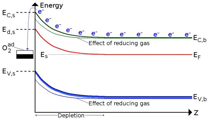
Metal oxide materials can be used as gas sensors, when heated to temperatures between 250 °C and 550 °C. At these temperatures, oxygen is adsorbed at the metal oxide surface by trapping electrons from the bulk material. The result is an overall decrease or increase in the metal oxide resistance, depending on whether the material is n-type or p-type, respectively. The band bending at the metal oxide/ambient interface is depicted in Figure 3. The introduction of a target gas in the atmosphere causes a reaction with the oxygen, removing it from the interface and reducing the band bending effect and, thereby, the overall resistance [26].
Figure 3.
Schematic representation of the band bending effect caused by oxygen adsorption and subsequent introduction of a reducing gas.
The thickness of the depletion layer is in the order of the Debye length, defined as:
| (1) |
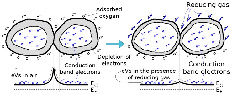
where ϵ0 is the free space permittivity, q is the elementary charge and nC is the carrier charge density The structure of the sensing layer will influence the sensing process. When a porous layer is deposited, the gas species can penetrate into the metal oxide to react at the surface of the grains and the grain boundaries [7], as shown in Figure 4. However, for compact metal oxide films, such as the ones studied here, the oxygen adsorption and reaction with a reducing gas occurs on the surface [26], as depicted in Figure 5.
Figure 4.
Gas sensing function and conduction mechanism for a porous metal oxide, where the oxygen and reducing gas can penetrate to interact with each grain.
Figure 5.

Gas sensing function for a compact tin oxide film. The reaction occurs only at the top surface of the deposited tin oxide. The symbol R refers to a reducing gas.
Even though plenty of effort has been directed towards understanding the gas sensing function of metal oxide materials, briefly addressed in Figures 4 and 5, the exact chemistry of the sensing process is complex and not yet exhaustively understood [27]. A porous film is more complex to deposit when compared to a compact thin film, usually involving a sol-gel technique followed by a gelation step [27]. A compact metal oxide thin film can be deposited using a variety of techniques, including spray pyrolysis, which has recently gained traction due to its cost-effectiveness and integration within a standard CMOS processing sequence. This study concerns itself with compact metal oxide thin films, and this section discusses the gas sensing capabilities achieved by various scientific research groups.
2.1. ZnO Gas Sensing Capability
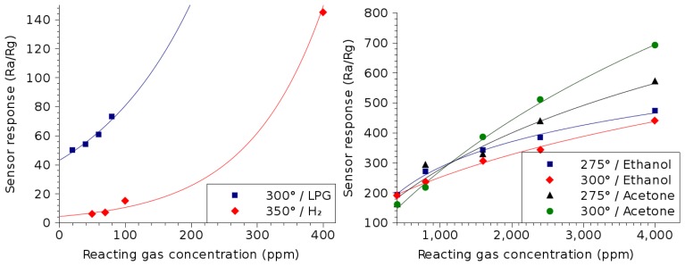
The capabilities of zinc oxide (ZnO) to detect hydrogen (H2), liquid petroleum gas (LPG), acetone ((CH3)2CO) and ethanol (C2H5OH) in the environment has been examined in the literature [28–30]. Acetone and ethanol belong to a group of organic chemicals referred to as volatile organic compounds (VOCs), which have a high vapor pressure at room temperature and often mix with interfering gases [31]. The sensor response is calculated by observing the resistance of the metal oxide layer in air (Ra) and dividing it by the resistance measured in the presence of the desired reacting gas (Rg). The temperature at which the sensitivities to ambient gases is examined reflects the peak temperature of operation for each thin film in the detection of the desired gas. The symbols given in Figure 6 represent the measured sensor responses, while the solid lines are best-fit lines, whose equations are given in Table 1.
Figure 6.
ZnO thin film sensor response dependence on the concentrations of various reacting gases. The temperatures used during measurement correspond to the optimal temperature of operation for the detection of the particular gas.
Table 1.
Summary of the gas sensing properties of ZnO, shown in Figure 6. The equation column shows the best-fit lines for the sensitivity of the thin film (solid lines in Figure 6).
| Reacting gas | Temperature | Equation | Concentration |
|---|---|---|---|
| Hydrogen (H2) [28] | 350 °C | 4.43 · e0.0088·Cppm | 50 ppm–400 ppm |
|
| |||
| Liquid petroleum gas (LPG) [29] | 300 °C | 43.1 · e0.0063·Cppm | 20 ppm–100 ppm |
|
| |||
| Acetone ((CH3)2CO) [30] | 275 °C | 382 · ln(Cppm + 1686) – 2737 | 400 ppm–4000 ppm |
| 300 °C | 710 · ln(Cppm + 2705) – 5561 | ||
|
| |||
| Ethanol (C2H5OH) [30] | 275 °C | 157 · ln(Cppm + 385) – 850 | |
| 300 °C | 290 · ln(Cppm + 2330) – 2100 | ||
From Figure 6 and Table 1, it is evident that ZnO can be used for the detection of several potentially dangerous gases, such as LPG, hydrogen, ethanol and acetone. For the detection of ambient hydrogen, an exponential behavior is noted, similar to the detection of LPG. The exponential response to the presence of a reacting gas is common during the early stages of detection, when the gas concentration is relatively low (<400 ppm). When the right side of Figure 6 is observed, a logarithmic dependence on the reacting gas concentration is noted. This is common when the concentration of the reacting gas is sufficiently high and moving towards saturation with respect to the ability to detect small variations.
From the acetone response in Figure 6, it is evident that below a concentration of about 1200 ppm, the response is stronger at an operating temperature of 275 °C, while above this concentration, 300 °C is preferable. This may be due to the fact that the sensing mechanism of acetone by metal oxides involves physisorption followed by chemisorption and electron transfer [32]. During physisorption, a surface acetone transfers to its isomer, which reacts with a second acetone to yield mesityl oxide; chemisorption and electron transfer can only take place thereafter [32]. When the concentration of acetone is low (below 1200 ppm), physisorption is the limiting step in the sensing mechanism, since two acetone molecules are required to generate mesityl oxide. Given that at this acetone concentration, a temperature of 275 °C is preferable, as shown in Figure 6, it can be deduced that the physisorption mechanism prefers a 275 °C operating temperature. On the other hand, chemisorption is the limiting step at acetone concentrations above 1200 ppm, which appears to prefer the higher 300 °C temperature.
2.2. In2O3 Gas Sensing Capability
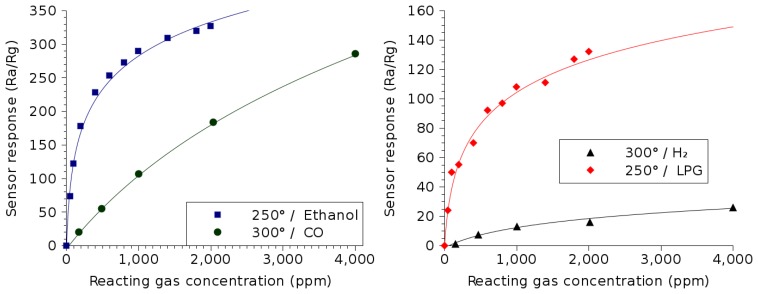
In addition to ethanol [33], LPG [33] and hydrogen [34], In2O3 thin films have been used to detect the presence of carbon monoxide (CO) down to 150 ppm [34]. The sensing capabilities of In2O3 thin films are shown in Figure 7. Once again, the symbols refer to the measured sensor response, while the solid lines are the lines of best fits, whose equations are given in Table 2.
Figure 7.
In2O3 thin film sensor response dependence on the concentrations of various reacting gases. The temperatures used during measurement correspond to the optimal temperature of operation for the detection of the particular gas.
Table 2.
Summary of the gas sensing properties of In2O3, shown in Figure 7. The equation column shows the best-fit lines for the sensitivity of the thin film (solid lines in Figure 7).
| Reacting Gas | Temperature | Equation | Concentration |
|---|---|---|---|
| Ethanol (C2H5OH) [33] | 250 °C | 74 · ln(Cppm + 21) – 230 | 50 ppm–2000 ppm |
| Liquid petroleum gas(LPG) [33] | 250 °C | 33 · ln(Cppm + 44.4) – 125 | |
|
| |||
| Carbon monoxide (CO) [34] | 300 °C | 246 · ln(Cppm + 1797) – 1848 | 150 ppm–4000 ppm |
| Hydrogen (H2) [34] | 300 °C | 11.6 · ln(Cppm + 435) – 72 | |
Similar to ZnO thin films, the overall trend for an In2O3 sensor is a logarithmic dependence on the reacting gas concentration and eventual saturation. For example, when the sensing response to ethanol and LPG is observed, it is clear that the sensing efficiency is highest with the gas concentration below about 1000 ppm. It can similarly be observed that the response to ambient hydrogen is weaker than to other reactive gases shown and that the ZnO film from Figure 6 is better suited for this particular function.
The In2O3 thin film responds very well to the presence of poisonous carbon monoxide in the environment. The response does not saturate even when 4000 ppm of CO is found in the sample ambient air. The film sensitivity appears almost linear, making for an almost ideal CO sensor, which is an essential part of every household, especially considering the odorless and colorless nature of CO gas.
2.3. ITO Gas Sensing Capability
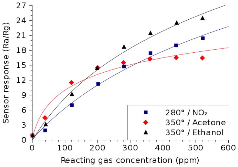
Indium-tin-oxide has frequently displayed its capability as a detector of ethanol [35], acetone [35] and methanol [31], detections of which frequently feature in ongoing attempts towards the development of the electronic nose [36]. In fact, some studies suggest that ITO thin films may offer a sufficiently strong detection of alcohol to allow operation even at room temperature [31]. However, here, we concentrate on sensor operation at elevated temperatures. The ITO thin film sensing response to the presence of acetone, ethanol and nitrogen dioxide (NO2), a harmful chemical when inhaled even at low concentrations, is shown in Figure 8.
Figure 8.
ITO thin film sensor response dependence on the concentrations of various reacting gases. The temperatures used during measurement correspond to the optimal temperature of operation for the detection of the particular gas.
The sensor response shown in Figure 8 mimics what was already seen in ZnO and In2O3 thin films. The general trend is a logarithmic dependence on the reactive gas concentration; the best-fit equations that govern this trend are given in Table 3. Figure 8 shows that the response to acetone saturates much sooner than the response to ethanol or NO2 presence, which appear to be detectable up to and potentially beyond 500 ppm.
Table 3.
Summary of the gas sensing properties of ITO, shown in Figure 8. The equation column shows the best-fit lines for the sensitivity of the thin film (solid lines in Figure 8).
2.4. SnO2 Gas Sensing Capability
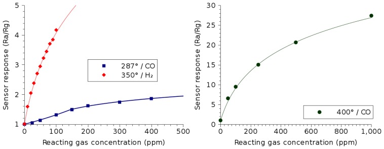
The gas sensing capability of SnO2 is well known, and it is the most common metal oxide used for the detection of harmful gases [37]. This is in part due to its sensitivity to a broad range of gases, but also due to the ability of the material to be deposited on a silicon substrate using a variety of simple and inexpensive methods. Figure 9 shows the response of a SnO2 thin film to the presence of hydrogen [16] and carbon monoxide (278 °C [38], 400 °C [39]) in the environment.
Figure 9.
SnO2 thin film sensor response dependence on the concentrations of various reacting gases. The temperatures used during measurement correspond to the optimal temperature of operation for the detection of the particular gas.
The SnO2 sensor response to the presence of CO shown in the left plot in Figure 9 has been measured at 287 °C for a sputtered film [38]. The CO response shown in the plot on the right has been measured at 400 °C for a film, which was deposited using a spray and includes impurities in the form of Pt nanoparticles [39]. The ability to deposit SnO2 films using a spray pyrolysis technique is further discussed in Section 4. The effect of the Pt impurity and higher operating temperature is noted by an increase in the sensing performance by almost ten times. Once again, the symbols in Figure 9 represent measured data, while the solid lines correspond to best-fit lines, the equations of which are given in Table 4. Another interesting observation with the sensing of CO at 287 °C is that the sensor response behavior switches from exponential below 150 ppm to logarithmic above 150 ppm; this is similar to the behavior noted in the ZnO film in Section 2.1.
Table 4.
Summary of the gas sensing properties of SnO2, shown in Figure 9. The equation column shows the best-fit lines for the sensitivity of the thin film (solid lines in Figure 9).
From Figure 9, the SnO2 film displays the ability to detect hydrogen at very low concentrations. While the hydrogen detection of ZnO films shown in Figure 6 appears to only start at a concentration of 100 ppm, SnO2 films can detect hydrogen down to 10 ppm [16].
3. Stress Evolution during Metal Oxide Deposition
During the deposition of metals and metal oxides on oxidized silicon surfaces, the film deposits in the form of islands, which coalesce and then grow to form larger grains, a process known as the Volmer–Weber growth mode [24,25]. The intrinsic stress generated during thin film growth develops during deposition and can go through stages of compressive and tensile stresses depending on the film properties. Figure 10 summarizes the main steps involved in the film growth, as characterized in [25].
Figure 10.

Steps during film formation using the Volmer–Weber growth mode. (a) 1-nucleation; (b) 2-impingement; (c) 3-coalescence; (d) 4a-columnar thickening; (e) 4b-polycrystalline thickening.
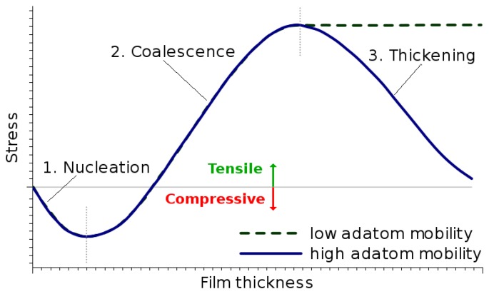
The initial stage is the island nucleation or the formation of small islands on the surface. As the islands grow, they impinge on each other, which generates tensile stress in the islands. When all of the islands on the surface are connected, a film is said to have coalesced. The next stage of growth is the film thickening, which can be either columnar or polycrystalline. The columnar thickening mode shown in Figure 10d refers to the growth of films that have a high adatom mobility or low melting temperatures, such as silver (Ag), copper (Cu) and aluminum (Al). The polycrystalline growth shown in Figure 10e refers to the growth of films that have a low adatom mobility or high melting temperatures, such as tungsten (W), chromium (Cr) and tantalum (Ta). Before film coalescence, there are two main stress components to consider, namely the compressive stress, which is generated due to the island nucleation, and the tensile stress generated in the thin film due to island impingement. The evolution of the stress during the growth of the two types of materials is shown in Figure 11. The generation of compressive stresses during nucleation and thickening, as well as the generation of a tensile stress during coalescence is depicted. The intrinsic stress of materials with low adatom mobility does not vary after coalescence and remains constant during thickening. However, materials with high adatom mobility experience a reduced stress, or increased compressive stress, during post-coalescence film growth.
Figure 11.
Stress evolution during the growth of metal and metal oxide films.
During the formation and subsequent radial expansion of an island during film growth, a compressive stress builds up due to an excess in surface energy. The model that governs the build-up of compressive stress in relation to the growth of an island is given in [25] as:
| (2) |
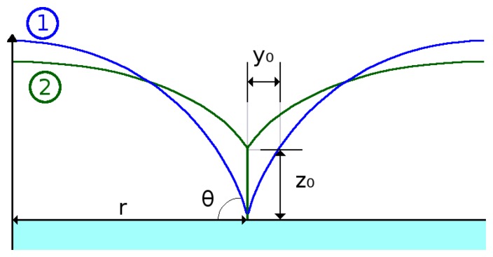
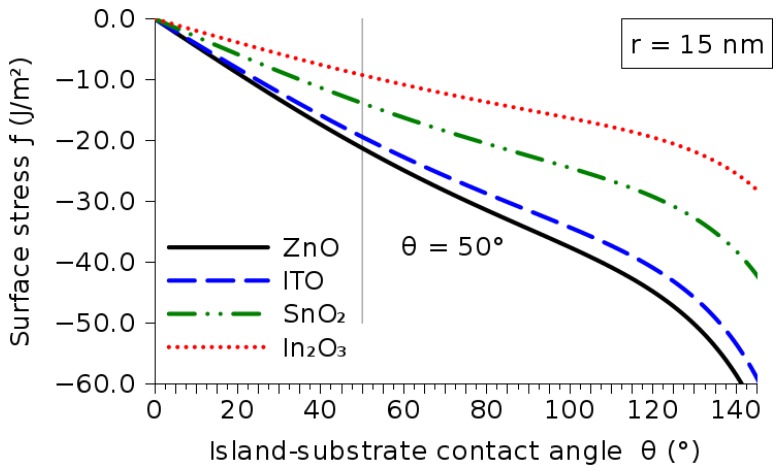
where f = γgb − 2γs is the surface stress (γgb is the grain boundary energy and γs is the surface energy), r is the island radius and θ is the contact angle between the island surface and the substrate, depicted in Figure 12. Upon island impingement, a grain boundary is formed between two islands, which results in a part of the free surface of each island being eliminated and in a significant energy reduction. This process of zipping at the grain boundary to a specific height generates tensile stress in the grains. Figure 12 shows the process of two islands impinging on each other and the formation of a grain boundary. When two islands approach each other and each attempts to increase its radius, a grain boundary forms. The generated tensile stress depends on the resulting geometry of that process, given in [25] as:
| (3) |
where E is the Young's modulus and r and y0 are geometric parameters given in Figure 12. When two islands come together (Step 1 in Figure 12) and they each attempt to grow, each island will be hindered by the presence of the adjacent island. Therefore, instead of freely expanding its circumference, a vertical boundary will form between them, with a height z0 (Step 2 in Figure 12).
Figure 12.
From Position 1 to Position 2, two islands impinge, resulting in a grain boundary with height z0.
The tensile stress described by Equation (3) can relax through the transport of matter to the strained region within the grain boundary. An equation that governs this mechanism is given in [25], and more details regarding the relaxation process can be found there:
| (4) |
where Co is a material-dependent parameter, h is the film thickness, Q is the activation energy for the material diffusion, k is the Boltzmann constant and T is temperature. For simplicity, the relaxation phenomena will be neglected here.
3.1. Metal Oxide Material Properties
The material properties required for the simulation of the post-processing intrinsic stress for metal oxides of interest are given in Table 5. The properties have been collected from a literature survey of [37,40–56]. It is important to note that the intrinsic stresses listed in Table 5 correspond to a compressive stress.
Table 5.
Properties of metal oxides ZnO, In2O3, indium-tin-oxide (ITO) and SnO2, required for the simulation of stress evolution during Volmer–Weber growth and grain coalescence. CTE, coefficients of thermal expansion.
| Characteristic | ZnO | In2O3 | ITO | SnO2 |
|---|---|---|---|---|
| Young's modulus E (GPa) | 210 [40] | 145 [41] | 116 [42] | 253 [43] |
| Poisson's ratio ν | 0.36 [44] | 0.31 [45] | 0.33 [46] | 0.293 [43] |
| CTE α (K−1) | 3.9 × 10 −6 [37] | 6.7 × 10⁻⁶ [37] | 8.5 × 10⁻⁶ [47] | 4.0 × 10⁻⁶[37] |
| Density ρ (g/cm3) | 5.67 [37] | 7.12 [37] | 7.18 [52] | 6.99 [37] |
| Average grain size D (nm) | 13–16.5 [49] | 10–80 [53,54] | 10–40 [55] | 12–16.5 [56] |
| Melting point (°C) | 2240 [37] | 2190 [37] | 1913 [52] | 1900 [37] |
| Intrinsic stress σi (GPa) | 2.3–3.43 [48,49] | 0.4–1.5 [50] | 2.1–2.3 [42] | 1.5 [51] |
3.2. Intrinsic Stress Generation during Metal Oxide Deposition
The build-up of compressive stress during deposition is described by Equation (2). The stress depends on the contact angle between the island surface and the substrate θ, the radius of the growing islands r and the surface stress f. The island radius r can be measured experimentally, and some published values are listed in Table 5. The expected compressive intrinsic stresses are also listed there; this allows an estimation of the expected surface stress for the metal oxides and an analysis of the dependence on the contact angle. Figure 13 shows the relationship between the surface stress and the contact angle for the metal oxides discussed in this manuscript. From Figure 13, it is evident that the surface stress decreases as the angle increases. At a sample angle of 50°, the surface stress for the metal oxides is given in Table 6.
Figure 13.
Relationship between the surface stress f (J/m2) and contact angle θ (°) during the deposition of the metal oxides ZnO, In2O3, ITO and SnO2.
Table 6.
Surface stress for the metal oxide materials introduced in this study. The average grain radius and island contact angle with the substrate are set to r = 15 nm and θ = 50°, respectively.
| Material: | ZnO | In2O3 | ITO | SnO2 |
|---|---|---|---|---|
| Intrinsic stress σi | 2.3 GPa | 1.0 GPa | 2.1 GPa | 1.5 GPa |
| Surface stress f | 21 J/m2 | 9 J/m2 | 19 J/m2 | 14 J/m2 |
Although most grown metal oxides exhibit compressive stresses in the GPa range, some authors have presented methods by which the stress can be reduced to several hundred MPa in the tensile regime. This reduction is mainly achieved by varying the process parameters during sputter deposition: an increase in the amount of oxygen in the environment for SnO2 films [51] and an increased pressure for ITO films [57] are examples. The resulting intrinsic stresses for the SnO2 and ITO films are 200 MPa and 300 MPa, respectively. Another manner by which the stress becomes more tensile is by annealing or material cooling after deposition at an increased temperature [57].
3.3. Thermo-Mechanical Stress during Metal Oxide Cooling
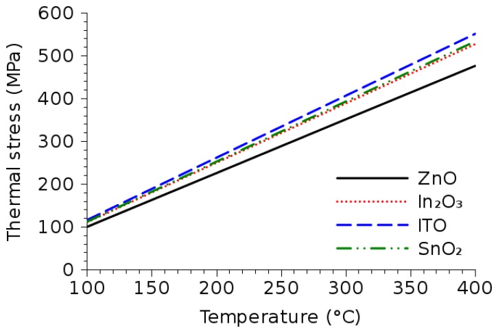
The amount of tensile stress generated due to heating depends on the CTEs of the materials involved. Using the values from Table 5 and assuming a deposition on a flat silicon wafer with a 500 nm-thick SiO2 isolation layer, the thermo-mechanical stresses are plotted in Figure 14; the values are derived using simulations with finite element programs. The temperature refers to the deposition or annealing temperature of the wafer prior to cooling to room temperature. The CTEs of silicon and SiO2 are 2.6 × 10⁻⁶ K−1 and 0.5 × 10⁻⁶ K−1, respectively.
Figure 14.
Thermo-mechanical stress for the metal oxide materials introduced in this study and its dependence on the process temperature. A linear dependence on temperature is evident. The metal oxide with the highest CTE (ITO) experiences the largest thermo-mechanical stress. Similarly, the metal oxide with the lowest CTE (ZnO) experiences the lowest stress.
When a temperature drop ΔT is imposed on a material, such as is the case during cooling to room temperature after a thermal deposition step, the material experiences a strain:
| (5) |
where α is the CTE. Therefore, the resulting stress is linear with respect to the applied temperature, as is observed in Figure 14. In addition, a larger CTE results in larger stress, which is also shown in Figure 14, where the metal oxide with the highest CTE (ITO) also experiences the highest thermo-mechanical stress. Similarly, the lowest CTE material (ZnO) experiences the lowest stress.
4. Spray Pyrolysis Deposition of SnO2
The deposition of SnO2 has been performed using various techniques, such as CVD [18], sputtering [19], pulsed-laser [20], sol-gel [21] and spray pyrolysis [15]. The spray pyrolysis technique has gained traction over its alternatives due to its cost effectiveness and ease of integration in the standard CMOS process. During deposition, a gas pressure nozzle is used to atomize a SnCl4+H2O solution. The nozzle generates very small droplets, which are directed towards the substrate, where SnO2 is deposited on top of a heated wafer, as shown in Figure 15. Using this method, substrates with complex geometries can be coated using CMOS-compatible temperatures at and below 400 °C. The nozzle is placed about 30 cm away from the substrate, ensuring that the droplets have no horizontal velocity when reaching the vicinity of the substrate. The long distance between nozzle and wafer also ensures that all large liquid droplets will be eliminated prior to reaching the substrate, ensuring a uniformity in the droplet size distribution and, thereby, a uniformity in the deposited film.
Figure 15.

Schematic of the experimental spray pyrolysis deposition process as set up for SnO2 deposition.
The steps that describe the processes taking place during spray pyrolysis deposition are [58]:
Atomization of the precursor solution;
Aerosol transport of the droplet;
Decomposition of the precursor to initiate film growth.
In this section, the dependence of the deposition time and temperature on the film thickness is described, and an empirical model for the growth of tin oxide films is introduced. In addition, the architecture of a SnO2 sensor is presented, and the model is implemented in order to generate a full sensor structure, useful for further simulation studies.
4.1. Model for Spray Pyrolysis Deposition
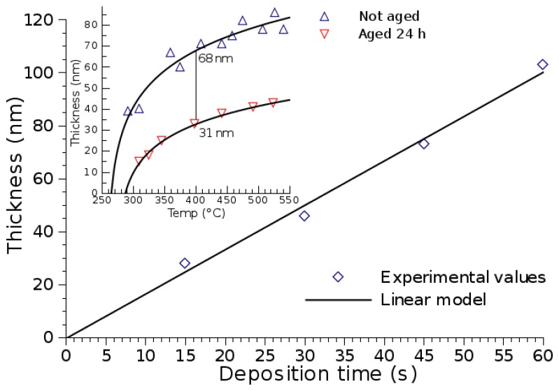
Several factors influence the film growth process, such as the distance between the nozzle and substrate, the length of the precursor solution aging, the air pressure, the solution volume, the temperature and the deposition time [4]. For the presented model, the ambient pressure, the nozzle distance to the substrate and the solution aging remain constant. In Figure 16, the dependence of the film thickness on the deposition time is shown, when the processing temperature is set to 400 °C. A linear relationship is evident, while a logarithmic dependence on the wafer temperature has also been observed [58]. An Arrhenius expression that best describes the deposition time (t, in seconds) and temperature (T, in Kelvin) dependence on the SnO2 thickness (d, in μm) is given by:
| (6) |
where A = 3.1 μm/s and E = 0.427 eV. A 50-nm thickness is reached after spray pyrolysis is performed for a 30-second burst at 400 °C. The inset of Figure 16 suggests that, depending on the solution aging, a 31-nm to 68-nm thickness is to be expected [4]. With a half-day aged solution, a 50-nm thickness is obtained under the same process conditions. When the technique is used to deposit a thin film on a step structure, no significant variation in the film thickness is noted [59]. This fact, combined with the high uniformity of the deposited film, means that the deposition occurs after the droplet approaches the heated substrate and forms a vapor. The droplets do not appear to directly impact the substrate surface in liquid form.
Figure 16.
Deposited SnO2 thickness versus deposition time. The inset shows the dependence of temperature and solution aging on the deposited thickness. A half-day aged solution is used in the given experiment.
4.2. Spray Pyrolysis Deposition on Gas Sensor Geometries
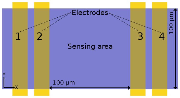
The sensing layer of a gas sensor is deposited on top of a substrate, which is provided with four electrodes, as shown in Figure 17. The full structure is placed on top of an electrically-insulating layer, which separates the substrate from a heater placed below it.
Figure 17.
Top view of the electrode locations on the substrate. The sensing area (SnO2) is deposited on top of the electrodes. The sensing area is 100 μm × 100 μm.
A two-dimensional view of a cut through the sensor geometry, including the electrode metals and passivation layer, is shown in Figure 18. The tin oxide deposition on the trench and step structure is modeled with Equation (6). The simulation of the deposition on complex geometries is performed using a Monte Carlo method within a level set framework [60]. A single particle species is considered during the deposition. As the simulation is initiated, multiple particles are generated with a flux in the direction of the substrate. Each particle is described by its arriving direction and energy, as well as its reflected direction and energy, should the particle not stick to its initial point of contact. It was found that a sticking coefficient of 0.01 has the best fit to experimentally-observed data. Figure 18 shows the resulting structure, when the spray pyrolysis deposition is simulated at 400 °C for 30 seconds. A uniform 50-nm SnO2 film covers the passivation and electrode layers.
Figure 18.
Geometry of the deposited SnO2 on the aluminum electrodes and silicon oxide passivation layers.
For a 50 nm-thick SnO2 layer, deposited using the spray pyrolysis technique, the X-ray diffraction pattern is given in [61]. When the deposition is performed at 400 °C, as was done in this study, the material exhibits polycrystalline peaks characteristic of the cassiterite phase [61]. The predominant reflections are from the crystallographic (110) and (200) planes, parallel to the substrate. In addition, small peaks are noted from other main planes of cassiterite (211), (101) or (211), indicating that the film has texture.
4.3. Gas Sensing Capability of the Sprayed SnO2 Film
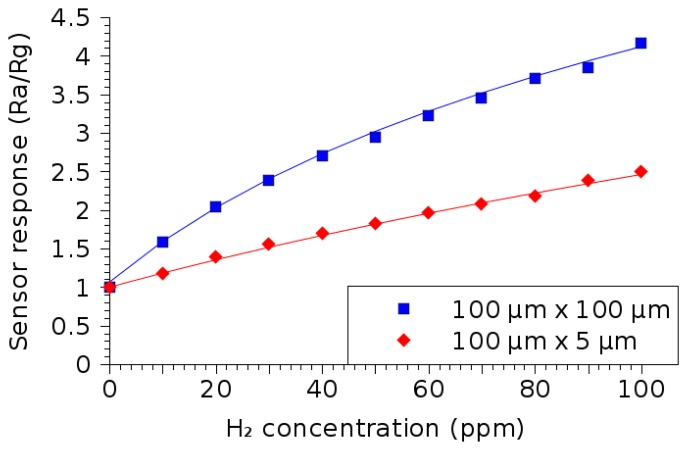
Two sensor structures have been used in order to test the sensor's response in the presence of H2 at a 350 °C temperature [16]. The dimensions of the two structures are 100 μm × 100 μm and 100 μm × 5 μm, respectively. A 50-nm layer of SnO2 has been deposited using spray pyrolysis, as described in the previous section. The effect of the presence of H2 in the atmosphere on the resistive response of the SnO2 layer is shown in Figure 19. It is evident that the sensor can detect the presence of hydrogen in the atmosphere down to 10 ppm. The symbols in the figure represent the measured sensor responses, while the solid lines represent the best-fit lines, the equations of which are given in Table 7.
Figure 19.
SnO2 thin film sensor response dependence on the concentration of hydrogen in the ambient gas. The 50-nm thin film is deposited using a spray pyrolysis burst of 30 s, while the wafer is heated to 400 °C. The sensing measurements are performed at 350 °C.
Table 7.
Equations corresponding to the best-fit curves for the measured data plotted in Figure 19. The sensor response displays a logarithmic dependence on the H2 concentration, as was previously noted in Section 2.
| Dimensions | 100 μm × 100 μm | 100 μm × 5 μm |
| Equation | 2.58 · ln(Cppm + 44.2) − 8.7 | 3.03 · ln (Cppm + 161.5) − 14.4 |
5. Summary and Conclusions
Smart gas sensors that can detect harmful and toxic gases in the environment have recently grown in popularity and research interest. While many CMOS and MEMS devices have experienced extreme miniaturization, gas sensors are still lagging in the form of bulky, power-intensive structures. The capability of metal oxides, such as ZnO, In2O3, ITO and SnO2, to detect various gases when heated to temperatures between 250 °C and 550 °C has recently been exploited in order to attempt to introduce gas sensors fit for wearable technologies. At these increased temperatures, the metal oxide material adsorbs oxygen at the surface, causing a depletion layer to form in the thin film. The result is an overall decrease or increase in the film resistance, depending on whether the material is n-type or p-type, respectively. When a target gas is introduced, it reacts with some of the surface oxygen, removing them from the film and thereby reducing the depletion layer and the film resistance. The difference between the resistance in air and the resistance in the presence of the reacting gas can then be exploited as the sensor response. ZnO, In2O3, ITO and SnO2 thin films have been examined for their ability to detect the presence of liquid petroleum gas, hydrogen, ethanol, acetone, carbon monoxide and nitrogen dioxide in the environment. The sensing reaction has a general logarithmic trend, which tends to saturate as more reacting gas interacts with the surface oxygen.
The stress generation during the deposition of metal oxides has also been examined. The post-processing stress is a combination of the intrinsic stress, which develops during the Volmer–Weber film growth, and the thermo-mechanical stress, which develops as a result of material cooling to room temperature from a thermal deposition step. The surface stress values for the analyzed films have been derived, and their dependence on the contact angle between the island surface and the substrate has been shown. The thermo-mechanical stress has been analyzed using finite element methods, and a linear relationship between the process temperature and the stress has been demonstrated.
Spray pyrolysis deposition has been introduced in order to generate a SnO2 sensor and to test its performance. A model for spray pyrolysis has been presented and implemented within a level set topography simulator. The film thickness shows a linear relationship with spray time and a logarithmic relationship with the process temperature. The generated sensor structure can be successfully used for the detection of hydrogen in the atmosphere down to 10 ppm.
Acknowledgements
Thank you to Giorgio C. Mutinati, Elise Brunet, Stephan Steinhauer and Anton Köck with the Austrian Institute of Technology for measurements and fruitful discussions.
Author Contributions
The product of this research and paper is an intellectual collaboration of both authors. The authors have equally contributed to the research concept, to the design of experiment, to the development of models and simulations, as well as to the writing of the final manuscript.
Conflicts of Interest
The authors declare no conflict of interest.
References
- 1.Meixner H., Lampe U. Metal oxide sensors. Sens. Actuators B Chem. 1996;33:198–202. [Google Scholar]
- 2.Frietsch M., Zudock F., Goschnick J., Bruns M. CuO catalytic membrane as selectivity trimmer for metal oxide gas sensors. Sens. Actuators B Chem. 2000;65:379–381. [Google Scholar]
- 3.Barsan N., Weimar U. Conduction model of metal oxide gas sensors. J. Electroceram. 2001;7:143–167. [Google Scholar]
- 4.Korotcenkov G., Brinzari V., Schwank J., DiBattista M., Vasiliev A. Peculiarities of SnO2 thin film deposition by spray pyrolysis for gas sensor application. Sens. Actuators B Chem. 2001;77:244–252. [Google Scholar]
- 5.Simon I., Bârsan N., Bauer M., Weimar U. Micromachined metal oxide gas sensors: Opportunities to improve sensor performance. Sens. Actuators B: Chem. 2001;73:1–26. [Google Scholar]
- 6.Comini E. Metal oxide nano-crystals for gas sensing. Anal. Chim. Acta. 2006;568:28–40. doi: 10.1016/j.aca.2005.10.069. [DOI] [PubMed] [Google Scholar]
- 7.Barsan N., Koziej D., Weimar U. Metal oxide-based gas sensor research: How to? Sens. Actuators B Chem. 2007;121:18–35. [Google Scholar]
- 8.Gardner J.W., Guha P.K., Udrea F., Covington J.A. CMOS interfacing for integrated gas sensors: A review. IEEE Sens. J. 2010;10:1833–1848. [Google Scholar]
- 9.Wang C., Yin L., Zhang L., Xiang D., Gao R. Metal oxide gas sensors: Sensitivity and influencing factors. Sensors. 2010;10:2088–2106. doi: 10.3390/s100302088. [DOI] [PMC free article] [PubMed] [Google Scholar]
- 10.Pijolat C. Metal oxide gas sensors. Chem. Sens. Biosens. 2012 doi: 10.1002/9781118561799.ch5. [DOI] [Google Scholar]
- 11.Ortel M., Trostyanskaya Y.S., Wagner V. Spray pyrolysis of ZnO-TFTs utilizing a perfume atomizer. Solid-State Electron. 2013;86:22–26. [Google Scholar]
- 12.Shinde S., Patil G., Kajale D., Gaikwad V., Jain G. Synthesis of ZnO nanorods by spray pyrolysis for H2S gas sensor. J. Alloys Compd. 2012;528:109–114. [Google Scholar]
- 13.Bouaoud A., Rmili A., Ouachtari F., Louardi A., Chtouki T., Elidrissi B., Erguig H. Transparent conducting properties of Ni doped zinc oxide thin films prepared by a facile spray pyrolysis technique using perfume atomizer. Mater. Chem. Phys. 2013;137:843–847. [Google Scholar]
- 14.Prasad M., Sahula V., Khanna V. Design and fabrication of Si-diaphragm, ZnO piezoelectric film-based MEMS acoustic sensor using SOI wafers. IEEE Trans. Semicond. Manuf. 2013;26:233–241. [Google Scholar]
- 15.Patil G., Kajale D., Gaikwad V., Jain G. Spray pyrolysis deposition of nanostructured tin oxide thin films. ISRN Nanotechnol. 2012;2012:275872:1–275872:5. [Google Scholar]
- 16.Mutinati G., Brunet E., Steinhauer S., Köck A., Teva J., Kraft J., Siegert J., Schrank F., Bertagnolli E. CMOS-integrable ultrathin SnO2 layer for smart gas sensor devices. Procedia Eng. 2012;47:490–493. [Google Scholar]
- 17.Brunet E., Maier T., Mutinati G., Steinhauer S., Köck A., Gspan C., Grogger W. Comparison of the gas sensing performance of SnO2 thin film and SnO2 nanowire sensors. Sens. Actuators B Chem. 2012;165:110–118. [Google Scholar]
- 18.Volintiru I., de Graaf A., Van Deelen J., Poodt P. The influence of methanol addition during the film growth of SnO2 by atmospheric pressure chemical vapor deposition. Thin Solid Films. 2011;519:6258–6263. [Google Scholar]
- 19.Boltz J., Koehl D., Wuttig M. Low temperature sputter deposition of SnOx:Sb films for transparent conducting oxide applications. Surf. Coat. Technol. 2010;205:2455–2460. [Google Scholar]
- 20.Sinha S., Bhattacharya R., Ray S., Manna I. Influence of deposition temperature on structure and morphology of nanostructured SnO2 films synthesized by pulsed laser deposition. Mater. Lett. 2011;65:146–149. [Google Scholar]
- 21.Carvalho D.M., Maciel J.L., Garcia R.E., Ferreira V.G., Scalvi L.V. Numerical simulation of the liquid phase in SnO2 thin film deposition by sol-gel-dip-coating. J. Sol-Gel Sci. Technol. 2010;55:385–393. [Google Scholar]
- 22.Siegele M., Gamauf C., Nemecek A., Mutinati G.C., Steinhauer S., Kock A., Kraft J., Siezert J., Schrank F. Optimized integrated micro-hotplates in CMOS technology. Proceedings of the IEEE 11th International New Circuits and Systems Conference; Paris, France. 16–19 June 2013. [Google Scholar]
- 23.Pletea M., Brückner W., Wendrock H., Kaltofen R. Stress evolution during and after sputter deposition of Cu thin films onto Si (100) substrates under various sputtering pressures. J. Appl. Phys. 2005;97:054908:1–054908:7. [Google Scholar]
- 24.Pletea M., Koch R., Wendrock H., Kaltofen R., Schmidt O. In situ stress evolution during and after sputter deposition of Al thin films. J. Phys.: Condens. Matter. 2009;21:225008:1–225008:8. doi: 10.1088/0953-8984/21/22/225008. [DOI] [PubMed] [Google Scholar]
- 25.Seel S.C. Ph.D. Thesis. Massachusetts Institute of Technology; Cambridge, MA, USA: 2002. Stress and Structure Evolution during Volmer-Weber Growth of Thin Films. [Google Scholar]
- 26.Barsan N., Weimar U. Fundamentals of Metal Oxide Gas Sensors. Proceedings of the 14th International Meeting on Chemical Sensors; Nuremberg, Germany. 20–23 May 2012; pp. 618–621. [Google Scholar]
- 27.Tiemann M. Porous metal oxides as gas sensors. Chemistry. 2007;13:8376–8388. doi: 10.1002/chem.200700927. [DOI] [PubMed] [Google Scholar]
- 28.Al-Salman H.S., Abdullah M. Fabrication and characterization of ZnO thin film for hydrogen gas sensing prepared by RF-magnetron sputtering. Measurement. 2013;46:1698–1703. [Google Scholar]
- 29.Mitra P., Chatterjee A.P., Maiti H.S. ZnO thin film sensor. Mater. Lett. 1998;35:33–38. [Google Scholar]
- 30.Li X., Chang Y., Long Y. Influence of Sn doping on ZnO sensing properties for ethanol and acetone. Mater. Sci. Eng. C. 2012;32:817–821. [Google Scholar]
- 31.Patel N., Patel P., Vaishnav V. Indium tin oxide (ITO) thin film gas sensor for detection of methanol at room temperature. Sens. Actuators B Chem. 2003;96:180–189. [Google Scholar]
- 32.Wang L., Kalyanasundaram K., Stanacevic M., Gouma P. Nanosensor device for breath acetone detection. Sens. Lett. 2010;8:709–712. [Google Scholar]
- 33.Zhan Z., Lu J., Song W., Jiang D., Xu J. Highly selective ethanol In2O3-based gas sensor. Mater. Res. Bull. 2007;42:228–235. [Google Scholar]
- 34.Yamaura H., Jinkawa T., Tamaki J., Moriya K., Miura N., Yamazoe N. Indium oxide-based gas sensor for selective detection of CO. Sens. Actuators B Chem. 1996;36:325–332. [Google Scholar]
- 35.Jiao Z., Wu M., Gu J., Sun X. The gas sensing characteristics of ITO thin film prepared by sol–gel method. Sens. Actuators B Chem. 2003;94:216–221. [Google Scholar]
- 36.Tamaki J., Maekawa T., Miura N., Yamazoe N. CuO-SnO2 element for highly sensitive and selective detection of H2S. Sens. Actuators B Chem. 1992;9:197–203. [Google Scholar]
- 37.Batzill M., Diebold U. The surface and materials science of tin oxide. Prog. Surf. Sci. 2005;79:47–154. [Google Scholar]
- 38.Di Giulio M., Micocci G., Rella R., Siciliano P., Tepore A. Properties of reactively sputtered tin oxide films as CO gas sensors. Sens. Actuators B Chem. 1995;23:193–195. [Google Scholar]
- 39.Mädler L., Sahm T., Gurlo A., Grunwaldt J.D., Barsan N., Weimar U., Pratsinis S. Sensing low concentrations of CO using flame-spray-made Pt/SnO2 nanoparticles. J. Nanoparticle Res. 2006;8:783–796. [Google Scholar]
- 40.Bai X., Gao P., Wang Z.L., Wang E. Dual-mode mechanical resonance of individual ZnO nanobelts. Appl. Phys. Lett. 2003;82:4806–4808. [Google Scholar]
- 41.Bartolomé J., Hidalgo P., Maestre D., Cremades A., Piqueras J. In-situ scanning electron microscopy and atomic force microscopy Young's modulus determination of indium oxide microrods for micromechanical resonator applications. Appl. Phys. Lett. 2014;104:161909:1–161909:5. [Google Scholar]
- 42.Neerinck D., Vink T. Depth profiling of thin ITO films by grazing incidence X-ray diffraction. Thin Solid Films. 1996;278:12–17. [Google Scholar]
- 43.Gladysz G., Chawla K. Coefficients of thermal expansion of some laminated ceramic composites. Compos. Part A Appl. Sci. Manuf. 2001;32:173–178. [Google Scholar]
- 44.Gadzhiev G. The thermal and elastic properties of zinc oxide-based ceramics at high temperatures. High Temp. 2003;41:778–782. [Google Scholar]
- 45.Zhang K., Regoutz A., Palgrave R., Payne D., Egdell R., Walsh A., Collins S., Wermeille D., Cowley R. Determination of the Poisson ratio of (001) and (111) oriented thin films of In2O3 by synchrotron-based X-ray diffraction. Phys. Rev. B. 2011;84:233301:1–233301:4. [Google Scholar]
- 46.Wittkowski T., Jorzick J., Seitz H., Schröder B., Jung K., Hillebrands B. Elastic properties of indium tin oxide films. Thin Solid Films. 2001;398:465–470. [Google Scholar]
- 47.Guo X., Jiang H., Li K.K., Zou Y.K. Heterostructure of Ferromagnetic and Ferroelectric Materials with Magneto-Optic and Electro-Optic Effects. US Patent 8,124,254. 2012
- 48.Water W., Chu S.Y. Physical and structural properties of ZnO sputtered films. Mater. Lett. 2002;55:67–72. [Google Scholar]
- 49.Ashida T., Kato K., Omoto H., Takamatsu A. Internal stress and microstructure of zinc oxide films sputter-deposited with carbon dioxide gas. Jpn. J. Appl. Phys. 2010;49:065501:1–065501:4. [Google Scholar]
- 50.Vygranenko Y., Wang K., Vieira M., Nathan A. Indium oxide thin-film transistor by reactive ion beam assisted deposition. Physica Status Solidi (a) 2008;205:1925–1928. [Google Scholar]
- 51.Boltz J. Ph.D. Thesis. Rheinisch-Westfälische Technische Hochschule Aachen; Aachen, Germany: 2011. Sputtered Tin Oxide and Titanium Oxide Thin Films as Alternative Transparent Conductive Oxides. [Google Scholar]
- 52.Narazaki A., Kurosaki R., Sato T., Niino H. On-demand patterning of indium tin oxide microdots by laser-induced dot transfer. Appl. Phys. Express. 2013;6:092601:1–092601:4. [Google Scholar]
- 53.Korotcenkov G., Brinzari V., Cerneavschi A., Ivanov M., Cornet A., Morante J., Cabot A., Arbiol J. In2O3 films deposited by spray pyrolysis: Gas response to reducing (CO, H2) gases. Sens. Actuators B Chem. 2004;98:122–129. [Google Scholar]
- 54.Gurlo A., Ivanovskaya M., Barsan N., Schweizer-Berberich M., Weimar U., Göpel W., Dieguez A. Grain size control in nanocrystalline In2O3 semiconductor gas sensors. Sens. Actuators B Chem. 1997;44:327–333. [Google Scholar]
- 55.Kulkarni A., Schulz K.H., Lim T., Khan M. Dependence of the sheet resistance of indium-tin-oxide thin films on grain size and grain orientation determined from X-ray diffraction techniques. Thin Solid Films. 1999;345:273–277. [Google Scholar]
- 56.Vuong D.D., Sakai G., Shimanoe K., Yamazoe N. Preparation of grain size-controlled tin oxide sols by hydrothermal treatment for thin film sensor application. Sens. Actuators B Chem. 2004;103:386–391. [Google Scholar]
- 57.Sasabayashi T., Ito N., Nishimura E., Kon M., Song P., Utsumi K., Kaijo A., Shigesato Y. Comparative study on structure and internal stress in tin-doped indium oxide and indium-zinc oxide films deposited by RF magnetron sputtering. Thin Solid Films. 2003;445:219–223. [Google Scholar]
- 58.Perednis D., Gauckler L. Solid oxide fuel cells with electrolytes prepared via spray pyrolysis. Solid State Ion. 2004;166:229–239. [Google Scholar]
- 59.Filipovic L., Selberherr S., Mutinati G., Brunet E., Steinhauer S., Köck A., Teva J., Kraft J., Siegert J., Schrank F., et al. Modeling the growth of tin dioxide using spray pyrolysis deposition for gas sensor applications. IEEE Trans. Semicond. Manuf. 2014;27:269–277. [Google Scholar]
- 60.Filipovic L., Selberherr S., Mutinati G.C., Brunet E., Steinhauer S., Köck A., Teva J., Kraft J., Siegert J., Schrank F., et al. A method for simulating spray pyrolysis deposition in the level set framework. Eng. Lett. 2013;21:224–240. [Google Scholar]
- 61.Korotcenkov G., DiBattista M., Schwank J., Brinzari V. Structural characterization of SnO2 gas sensing films deposited by spray pyrolysis. Mater. Sci. Eng. B. 2000;77:33–39. [Google Scholar]


