Abstract
We investigated the surface work function (WS) and its spatial distribution for epitaxial VO2/TiO2 thin films using Kelvin probe force microscopy (KPFM). Nearly grain-boundary-free samples allowed observation of metallic and insulating domains with distinct WS values, throughout the metal–insulator transition. The metallic fraction, estimated from WS maps, describes the evolution of the resistance based on a two-dimensional percolation model. The KPFM measurements also revealed the fractal nature of the domain configuration.
Some metal oxides exhibit first-order phase transitions, in which different electronic and magnetic phases coexist during the transition1. Interplay among the charge, spins, lattice, and orbitals influences the spatial distribution of the different phase domains. Evolution of such domain maps under external stimuli, including heat2,3, electric and magnetic fields2,3,4,5,6,7,8, optical excitation9,10, and strain11,12,13,14,15, results in a huge change in the electrical resistance and/or optical response; one of the most notable examples is the colossal magnetoresistance in manganite thin films2,8. Theoretical studies of these fascinating phenomena have suggested that the oxides are intrinsically inhomogeneous on the nanoscale, owing to strong electronic correlations16.
VO2 exhibits metal–insulator transitions (MITs) and structural phase transitions near room temperature1. The coexistence of metallic and insulating domains in VO2 thin films and its influence on the physical properties have been investigated extensively3,6,7,9,10,11,12,13,14,15,16,17,18,19,20,21,22,23,24,25,26,27,28,29,30,31. Analyses of the macroscopic physical properties of VO2 often require careful consideration of the geometric configuration of the domains. Recently, Ramíez et al. and Aliev et al. reported anomalous behavior in AC impedance spectra of VO2 thin films22,23. These experimental data suggest that ultra-thin, highly conductive domains exist below the transition temperature, and that the domain boundaries have a fractal nature near the transition temperature. According to percolation theory, metallic clusters form a fractal surface32, which can explain the impedance spectra; however, there has been no explicit experimental evidence for this to date. The domain configurations significantly affect the phase transition behavior of VO2 thin films, as well as the performance of prototypical devices based on VO2 thin films, including a split-ring-resonator-based metamaterials17, active terahertz nanoantennas18, ultra-thin perfect absorbers19, and phase-transition-driven memristive systems20.
Thermal and lattice mismatch between films and substrates can induce tensile or compressive strain, and accumulated elastic distortion often generates grain boundaries (GBs) in thin films. It has been reported that the phase transition behaviors of VO2 thin films largely vary depending on their strain states12,15. Moreover, GBs in VO2 thin films show distinct conduction properties compared with the intra-grain region25. Recently, several research groups successfully prepared very thin, nearly GB-free VO2 thin films on TiO2 substrates, taking advantage of the small lattice mismatch7. In this regard, VO2/TiO2 thin films provide an ideal system for studying the intrinsic two-dimensional (2D) phase transition characteristics of VO2.
All of these considerations raise the following question: How can we directly observe the metallic and insulating domain configurations of VO2 thin films and their evolution throughout the transition? Conventional x-ray diffraction (XRD), photoemission spectroscopy, and optical spectroscopies can be used to investigate the physical properties of VO2 during the MIT21; however, these techniques provide only the physical quantities averaged at the macroscopic scale. Nanoscale probe-based tools, such as scanning tunneling microscopy (STM) and scanning probe microscopy (SPM), have superior spatial resolution. Various SPM-based techniques have been developed to probe the electrical properties of samples. In particular, Kelvin probe force microscopy (KPFM) is a versatile tool for investigating the local surface potential under ambient conditions31,33.
In this work, we demonstrated that KPFM measurements of the local surface work function (WS) can be used to reveal the intriguing phase transition behaviors of the VO2/TiO2 thin films. The WS maps clearly show the spatial distribution of metallic and insulating domains during the transition. The evolution of the metallic domain fraction well explains the temperature dependence of the resistivity based on the 2D percolation model. The domain size is tens of nanometers at intermediate temperatures. The perimeter and area of the metallic domains follow power-law behaviors: a power exponent larger than 1/2 suggests that the metallic domains are fractal objects.
Figure 1 shows the XRD pattern for the 15-nm-thick VO2 thin film grown on a TiO2 (001); two significant peaks corresponding to tetragonal VO2 (002) at the higher angle and TiO2 (002) at the lower angle were evident. The cross-sectional high-resolution transmission electron microscopy (HR-TEM) image shown in the inset of Fig. 1 confirms the epitaxial crystallinity. Previously, we reported details of the sample preparation procedures and characterization results7.
Figure 1.
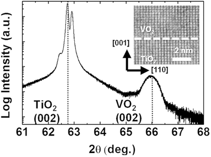
An x-ray diffraction (XRD) pattern of a 15-nm-thick VO2 thin film grown on a TiO2(001) substrate. The inset shows a cross-sectional high-resolution transmission electron microscopy (HR-TEM) image of the VO2/TiO2 thin film.
Figure 2a shows a schematic diagram of the measurement setup. Transport and KPFM measurements (XE-100, Park Systems) can be simultaneously performed in a glove box filled with N2 gas. The sample temperature was varied from 285 to 355 K using a sample stage equipped with a Peltier device. The VO2 thin film was patterned by photolithography and reactive ion etching with SF6 gas. The width and length of the stripe-shaped pattern were 4 and 30 μm, respectively.
Figure 2.
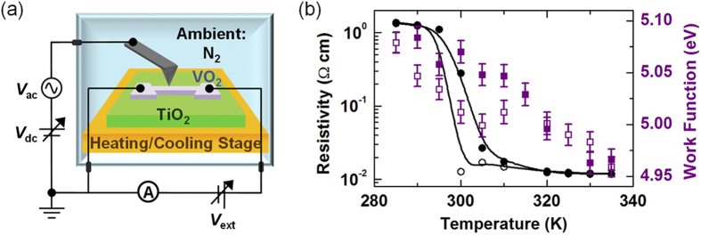
(a) Schematic illustration of the transport and Kelvin probe force microscopy (KPFM) measurement setup. (b) The resistivity (circles) and work function (squares) as a function of temperature for the VO2/TiO2 film. The filled symbols indicate data obtained during heating cycles, and the open symbols indicate data obtained during cooling cycles.
Figure 2b shows the resistivity (ρ) and surface work function (WS) measured during a heating and cooling cycle. WS was averaged over a 2 × 1-μm2 scanned area on the VO2 surface. ρ undergoes an abrupt change around 300 K. The transition temperature (TC) is less than that of a single crystal, due to the shorter c-axis length caused by epitaxial strain28. WS gradually decreases (increases) while raising (lowering) the sample temperature, indicating variation in the electronic structure. The temperature dependences of both ρ and WS were reproducible under repeated heating and cooling cycles. Thus, although surface redox must be accounted for under ultra-high-vacuum conditions29, it was not a consideration in this study.
Figure 3a-d show the WS maps obtained from an identical region, whose morphology is shown in Fig. 3e, while heating the sample from 285 to 355 K. The sample surface was very flat; the root-mean-square roughness was only 0.42 nm. Hence, topographic artifacts had little effect on the WS images. From Fig. 2b, two values (i.e., 5.06 and 4.96 eV) can be chosen as representative values for low- and high-temperature WS, respectively. The two values correspond to blue and red colors in the WS maps shown in Fig. 3a–d; as the temperature increased, the area of the red (blue) region decreased (increased). Note that the VO2 surface regions were either red or blue in color only, with the exception of the boundary region between the two colors. In contrast, our earlier study showed that the VO2/Al2O3 films exhibited a gradual change of WS over the entire surface area with variations in the sample temperature31. The VO2/Al2O3 films suffer from rather large strain due to the lattice mismatch, generating high-density GBs and tens-of-nm-sized grains. The domain size should be limited by the GBs and the width of the space charge region (SCR) formed at the boundaries of the metallic and insulating domains, which can cover large portions of the sample surface area during the transition31. Consequently, we expect that band bending at the domain boundaries would dominate the spatial distribution and temperature evolution of WS in the VO2/Al2O3 film with small grains. A comparison of VO2/TiO2 (this work) and VO2/Al2O3 (Ref. 31) thin films showed that distinct strain states and resulting microstructures can significantly influence the evolution of the WS maps in the VO2 thin films.
Figure 3.

Work function maps at (a) 285, (b) 305, (c) 335, and (d) 355 K during heating. The color scale is the same for all images. The larger work function (red) represents the insulating phase and the smaller work function (blue) represents the metallic phase. (e) The surface morphology of the region used to obtain the work function maps. The scale bar is 100 nm.
Kelvin probe force microscopy is based on the electrostatic interaction between the probe tip and sample, and has a spatial resolution of tens of nm34. Some of the intermediate regions shown in Fig. 3a–d might be caused by the limited spatial resolution of KPFM; however, the dimensions of some of the intermediate-work-function regions (shown by the green regions in Fig. 3a–d) are significantly larger than the spatial resolution limit and red spots can be seen at the center of such green regions. The limited resolution alone may not explain such results. Therefore, the intermediate regions in the work function maps should be explained by the SCR formation at the domain boundaries as well as the resolution limit of KPFM.
Near-field scanning optical microscopy (NSOM)3 and hard x-ray nanoprobe (HXN) measurements30 revealed metallic and insulating domains in the VO2 thin films as they underwent the MIT. In both NSOM and HXN data, the spectra and diffraction patterns near TC were broader than those far from TC, implying the coexistence of the two phases; however, extraction of a physical parameter from individual domains is not straightforward. The dielectric constant from optical spectra and the lattice constant from diffraction patterns can be obtained only after model-based fittings, in which the associated sample states and fitting parameters are chosen subjectively. In contrast, KPFM results provide the local surface work function of a specific area without the need for numerical analysis.
From the map for each temperature, the metallic region can be identified as the region with the high-temperature WS (i.e., the blue-colored region in Fig. 3a–d). The typical size (tens of nm) and the shape of the metallic domain were similar to those obtained from the NSOM and HXN results3,30. The area with the high-temperature WS enables us to estimate the metallic fraction, PM. PM increases linearly with the sample temperature. Interestingly, the metallic domains (the blue region) were present even at 285 K, far below TC (Fig. 3a). Ramirez et al. suggested the existence of persistent metallic domains in VO2 from analysis of the resistance hysteresis during the MIT27. Additionally, a small part of the sample surface had a low-temperature WS even at 355 K, far above TC(the red region in Fig. 3d); this may correspond to an area where stain relaxation occurs, stabilizing the insulating phase at high temperatures26.
Figure 4a and 4b show the difference in WS between high and low temperatures. The average WS decreased as the temperature increased (see Fig. 2b), and hence we would expect local WS to be smaller at high temperatures than at low temperatures (see the dark color in Fig. 4a and 4b). From Fig. 4a and 4b, however, in some localized regions (see light colored regions) we can see that WS increased with temperature. This suggests that an inverse phase transition (i.e., from insulating to metallic phases) occurred in these local areas. Qazilbash et al. observed a similar inverse phase transition at the nanoscale in HXN experiments30. Our data appear to show relevant experimental results, although a clear understanding of the physical origin is currently lacking.
Figure 4.
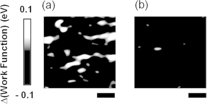
Maps of the difference in the work function (WS) at different temperatures. (a) WS(305 K)—WS(285 K) and (b) WS(355 K)—WS(285 K). The scale bar is 100 nm.
Figure 5a shows the full-width-half-maximum (FWHM) of the WS distributions as a function of temperature. Figure 5b shows histograms of WS at 285, 305, and 355 K; PM gradually increased with the sample temperature, as expected from the progressive decrease in WS (see Fig. 1c). The FWHM exhibited a broad single peak centered at 305 K, corresponding to a PM value of nearly 1/2. When the metallic and insulating domains have nearly the same area, WS will experience its highest standard deviation, and the FWHM was a maximum.
Figure 5.
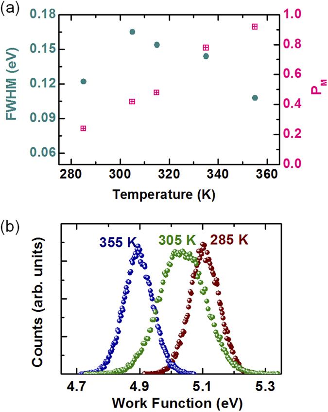
(a) The full-width-half-maximum (FWHM) of the work function distributions and metallic fraction (PM) as a function of temperature. (b) Work function histograms for sample temperatures of 285, 305, and 355 K.
Figure 6 shows the sample conductivity, σ, as a function of PM obtained from the WS maps. σ, increases abruptly at PM ~ 0.3. The percolation model can be applied to describe the relationship between σ, and PM, as reported previouly7,21. According to the percolation model, σ, should have a power-law dependence as a function of PM, i.e., σ, ∝ (PM – PC)t, where PC is the percolation threshold and t is the critical exponent32. The universal values are PC = 0.45 and t = 1.4, for the 2D percolation conduction model, and 0.15 < PC < 0.17 and t = 2.0, for the 3D percolation model7,21,32. The PM dependence of σ, can is described well by the 2D percolation model with PC = 0.36 and t = 1.46, as shown in the inset of Fig. 6. These values are similar to those reported from optical microscopy measurements7 of epitaxial VO2/TiO2 thin films. These results suggest that the value of PM from our KPFM measurements accurately describes the metallic fraction in the VO2/TiO2 thin films.
Figure 6.
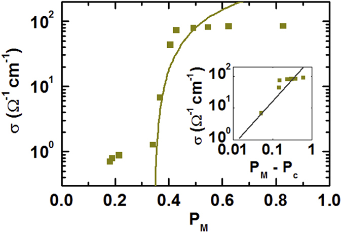
The conductivity, σ, as a function of PM during heating. The solid line fits the data correspond to the two-dimensional (2D) percolation model, σ, ∝ (PM – PC)t; the inset shows a log-log plot of σ, versus (PM – PC), where PC is the percolation threshold.
Chang et al. reported that PM, estimated from scanning tunneling spectroscopy (STS) experiments deviated significantly from that obtained from XRD data21. STS is a technique used to study the surface density of states; atomic resolution can be achieved with this technique for well-prepared surfaces. VO2 has very strong electron-lattice coupling and correlation effects; hence, the surface physical properties can be altered significantly from the bulk properties21. However, the surface preparation procedures to obtain atomically ordered oxide surfaces have not been well established35. In particular, it can be difficult to achieve oxygen stoichiometry at the oxide surface in ultrahigh vacuum29, thus, inherent features of metal oxides can limit observation of intrinsic MIT behavior in VO2 using STS analysis.
Figure 7 shows that the relationship between the perimeter (Σ) and area (A) of metallic domains at 285, 305, and 335 K follows a power law; specifically, log(Σ) ∝ log(A). More interestingly, the data for the three temperatures overlapped a single line. The power exponent, i.e., the slope in the log(Σ)-log(A) plot, was estimated to be 0.74. Objects with Euclidian shapes should have a slope of 0.5, because A ∝ Σ2. Thus, the larger exponent suggests that the metallic domains are fractal objects, having a fractal dimension, D = 1.48 (i.e., Σ ∝ A1.48/2). The percolation cluster is known to be an example of a random fractal32, and our KPFM measurements provide direct evidence for the fractal nature of the domain shapes in VO2.
Figure 7.
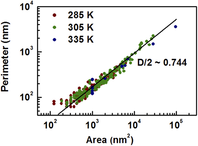
Log-log plots of the perimeters (Σ) of the metallic domains as a function of their area (A) at 285 K (<TC), 305 K (~TC), and 335 K (>TC). A single fit well describes the power-law behavior between Σ and A obtained at these temperatures. The slope of the log(Σ)-log(A) plot was 0.74; a value greater than 0.5 indicates a fractal nature of the domain shapes.
Simultaneous measurements of WS and the resistivity of VO2/TiO2 thin films in this study provided information on the temperature-dependent domain configurations and their influence on MIT behaviors. The local surface WS of a specific area was measured directly using KPFM, without the need for additional numerical analysis. WS maps, obtained by KPFM, showed that the nearly GB-free VO2/TiO2 thin films had tens-of-nm-sized metallic and insulating domains with clearly distinct WS values, throughout the MIT transition. The 2D percolation model well explains the relationship between the metallic domain fraction and the sample resistivity. Real-space domain maps also suggest that the domains form a fractal surface, which is a well-known feature of percolation clusters.
Methods
VO2 thin films that were 15-nm-thick were deposited on rutile TiO2 (001) substrates using pulsed laser deposition using an ArF Excimer laser with a wavelength of λ = 193 nm, a repetition rate of 2 Hz, and a fluence of 10 mJ cm−2 at 430 °C in an 1.0-Pa oxygen atmosphere. A V2O5 pellet was used as the target, and the deposition rate was approximately 0.3 nm min−1. KPFM measurements were made using an atomic force microscope (XE-100, Park Systems) with a glove box. The glove box was purged using N2 for more than 3 hours, and the sample was then heated to 100 °C for 30 min to remove any adsorbed water. The KPFM and transport measurements were then carried out while varying the sample temperature using a Peltier device. Conductive Pt-coated Si cantilevers with a resonance frequency of ~240 kHz (NSG10/Pt, NT-MDT) were used to characterize the work function and topography. Immediately following each measurement, the work function of the tip was calibrated using highly ordered pyrolytic graphite (HOPG) (SPI Supplies) as a reference sample. The measurements were repeated several times and no noticeable differences were observed, confirming the reproducibility of the data. For the transport experiments, Al wires were bonded at the ends of a striped pattern using a wire bonder (7476D, West Bond). Two-probe electrical measurements were performed using a semiconductor parameter analyzer (4156B, Hewlett Packard) simultaneously with the work function measurements.
Author Contributions
A.S. and D.K. performed the measurements and analyzed the data. T.K., K.S. and H.T. prepared and characterized the samples. All authors discussed the results and commented on the manuscript.
Additional Information
How to cite this article: Sohn, A. et al. Fractal Nature of Metallic and Insulating Domain Configurations in a VO2 Thin Film Revealed by Kelvin Probe Force Microscopy. Sci. Rep. 5, 10417; doi: 10.1038/srep10417 (2015).
Acknowledgments
A.S. and D.K. acknowledge the support from Basic Science Research Program and the Quantum Metamaterials Research Center (QMMRC) through the National Research Foundation of Korea Grant (NRF-2013R1A1A2063744, NRF-2008-0061893). T.K., K.S. and H.T. acknowledge the support from Grant-in-Aid for Scientific Research A (No. 26246013) and Grant-in-Aid for Scientific Research B (No. 25286058) from the Japan Society for Promotion of Science (JSPS), and the Nanotechnology Platform Project (Nanotechnology Open Facilities in Osaka University) of MEXT (F-14-OS-0010, S-14-OS-0007).
References
- Imada M. et al. Metal-insulator transitions. Rev. Mod. Phys. 70, 1039–1263 (1998). [Google Scholar]
- Fäth M. et al. Spatially inhomogeneous metal-insulator transition in doped manganites. Science 285, 1540–1542 (1999). [DOI] [PubMed] [Google Scholar]
- Qazilbash M. M. et al. Mott transition in VO2 revealed by infrared spectroscopy and nano-imaging. Science 318, 1750–1753 (2007). [DOI] [PubMed] [Google Scholar]
- Lai K. et al. Mesoscopic percolating resistance network in a strained manganite thin film. Science 329, 190–193 (2010). [DOI] [PubMed] [Google Scholar]
- Nakano M. et al. Collective bulk carrier delocalization driven by electrostatic surface charge accumulation. Nature 487, 459–462 (2012). [DOI] [PubMed] [Google Scholar]
- Driscoll T. et al. Current oscillations in vanadium dioxide: Evidence for electrically triggered percolation avalanches. Phys. Rev. B 86, 094203 (2012). [Google Scholar]
- Kanki T. et al. Direct observation of giant metallic domain evolution driven by electric bias in VO2 thin films on TiO2(001) substrate. Appl. Phys. Lett. 101, 243118 (2012). [Google Scholar]
- Becker T. et al. Intrinsic inhomogeneities in manganite thin films investigated with scanning tunneling spectroscopy. Phys. Rev. Lett. 89, 237203 (2002). [DOI] [PubMed] [Google Scholar]
- Morrison V. R. et al. A photoinduced metal-like phase of monoclinic VO2 revealed by ultrafast electron diffraction. Science 346, 445–448 (2014). [DOI] [PubMed] [Google Scholar]
- Hilton D. J. et al. Enhanced photosusceptibility near Tc for the light-induced insulator-to-metal phase transition in vanadium dioxide. Phys. Rev. Lett. 99, 226401 (2007). [DOI] [PubMed] [Google Scholar]
- Favaloro T. et al. A. Direct observation of nanoscale Peltier and Joule effects at metal−insulator domain walls in vanadium dioxide nanobeams. Nano Lett. 14, 2394–2400 (2014). [DOI] [PubMed] [Google Scholar]
- Fan L. L. et al. Strain dynamics of ultrathin VO2 film grown on TiO2 (001) and the associated phase transition modulation. Nano Lett. 14, 4036–4043 (2014). [DOI] [PubMed] [Google Scholar]
- Wu J. et al. Strain-induced self organization of metal-insulator domains in single-crystalline VO2 nanobeams. Nano Lett. 6, 2313–2317 (2006). [DOI] [PubMed] [Google Scholar]
- Hu B. et al. Self-heating and external strain coupling induced phase transition of VO2 nanobeam as single domain switch. Adv. Mater. 23, 3536–3541 (2011). [DOI] [PubMed] [Google Scholar]
- Kikuzuki T. et al. Strained state dynamics in a VO2 thin film. Phys. Rev. B 82, 144113 (2010). [Google Scholar]
- Shenoy V. B. et al. Electronic phase separation in correlated oxides: the phenomenon, its present status and future prospects. Chem. Phys. Chem. 7, 2053–2059 (2006). [DOI] [PubMed] [Google Scholar]
- Appavoo K. & Haglund R. F. Jr. Detecting nanoscale size dependence in VO2 phase transition using a split-ring resonator metamaterial. Nano Lett. 11, 1025–1031 (2011). [DOI] [PubMed] [Google Scholar]
- Seo M. et al. Active terahertz nanoantennas based on VO2 Phase Transition. Nano Lett. 10, 2064–2068 (2010). [DOI] [PubMed] [Google Scholar]
- Kats M. A. et al. Ultra-thin perfect absorber employing a tunable phase change material. Appl. Phys. Lett. 101, 221101 (2012). [Google Scholar]
- Driscoll T. et al. Phase-transition driven memristive system. Appl. Phys. Lett. 95, 0435031 (2009). [Google Scholar]
- Chang Y. J. et al. Surface versus bulk characterizations of electronic inhomogeneity in a VO2 thin film. Phys. Rev. B 76, 075118 (2007). [Google Scholar]
- Ramírez J.-G. et al. Ultra-thin filaments revealed by the dielectric response across the metal-insulator transition in VO2. Appl. Phys. Lett. 102, 063110 (2013). [Google Scholar]
- Aliev V. S. et al. Anomalous large electrical capacitance of planar microstructures with vanadium dioxide films near the insulator-metal phase transition. Appl. Phys. Lett. 104, 132906 (2014). [Google Scholar]
- Kar A. et al. Intrinsic electronic switching time in ultrathin epitaxial vanadium dioxide thin film. Appl. Phys. Lett. 102, 072106 (2013). [Google Scholar]
- Yang T.-H. et al. Role of twin boundaries in semiconductor to metal transition characteristics of VO2 films. Appl. Phys. Lett. 97, 07210 (2010). [Google Scholar]
- Kawatani K. et al. Formation mechanism of a microscale domain and effect on transport properties in strained VO2 thin films on TiO2(001). Phys. Rev. B 90, 054230 (2014). [Google Scholar]
- Ramírez J.-G. et al. First-order reversal curve measurements of the metal-insulator transition in VO2: Signatures of persistent metallic domains. Phys. Rev. B 79, 235110 (2009). [Google Scholar]
- Muraoka Y. & Hiroi Z. Metal–insulator transition of VO2 thin films grown on TiO2 (001) and (110) substrates. Appl. Phys. Lett. 80, 583–585 (2002). [Google Scholar]
- Yin W. et al. Nanoscale probing of electronic band gap and topography of VO2 thin film surfaces by scanning tunneling microscopy. J. Appl. Phys. 109, 024311 (2011). [Google Scholar]
- Qazilbash M. M. et al. Nanoscale imaging of the electronic and structural transitions in vanadium dioxide. Phys. Rev. B 83, 165108 (2011). [Google Scholar]
- Sohn A. et al. Evolution of local work function in epitaxial VO2 thin films spanning the metal-insulator transition. Appl. Phys. Lett. 101, 191605 (2012). [Google Scholar]
- Stauffer D. & Aharony A. Introduction to Percolation Theory ; Taylor & Francis: London, 1992. [Google Scholar]
- Kim H. et al. Enhanced surface-and-interface coupling in Pd-nanoparticle-coated LaAlO3/SrTiO3 heterostructures: strong gas- and photo-induced conductance modulation. Sci. Rep. 5, 8531; DOI: 10.1038/srep08531 (2015). [DOI] [PMC free article] [PubMed] [Google Scholar]
- Sadewasser S. & Glatze (Eds.), T. Kelvin probe force microscopy: measuring and compensating electrostatic forces, Sprigner, Heidelberg, 2011. [Google Scholar]
- Henrich V. E. & Cox P. A. The Surface Science of Metal Oxides ; Cambridge University Press: Cambridge, 1996. [Google Scholar]


