

Abstract
Progresses in the design of well-defined electronic band structure and dedicated functionalities rely on the high control of complex architectural device nano-scaled structures. This includes the challenging accurate description of strain fields in crystalline structures, which requires non invasive and three-dimensional (3D) imaging methods. Here, we demonstrate in details how x-ray Bragg ptychography can be used to quantify in 3D a displacement field in a lithographically patterned silicon-on-insulator structure. The image of the crystalline properties, which results from the phase retrieval of a coherent intensity data set, is obtained from a well-controlled optimized process, for which all steps are detailed. These results confirm the promising perspectives of 3D Bragg ptychography for the investigation of complex nano-structured crystals in material science.
Strain fields in semiconductors are long proposed as a route for the design of well-defined electronic properties in microelectronic devices1. It relies on the modification of the electronic band structure, reported for instance in silicon2 or in germanium3,4. The case of the integration of strained semiconductors to the widely used silicon-on-insulator (SOI) technology is of particular importance as the SOI technology offers the production of high-quality low-cost substrates associated to gains in device design, electronic performance and scalability5. In this context, the precise control of strain is mandatory. It includes the detailed knowledge of the crystal lattice behavior within a given nanostructure morphology and with regards to the fabrication process. Indeed, not only the presence of surfaces and interfaces is susceptible to dramatically alter the expected electronic design, but the nanostructure elaboration itself6. This calls for experimental methods able to image the crystalline properties in three dimensions (3D), over a large field of view, within a nanometer resolution and -ideally- in a non-pertubative way. Experimental approaches such as transmission electron microscopy7, x-ray Bragg nano-diffraction8and finite-support Bragg coherent diffraction imaging9are well-established techniques for strain analysis. They however only partly fulfill the required specifications justifying the development of an imaging approach capable of entirely answering this need.
The microscopy technique that we promote, namely Bragg ptychography, is an extension of the ptychography method which was originally implemented for electron microscopy applications10. It makes use of multiple exposures that combine redundant information from partially overlapping illumination areas onto an extended sample11. A set of partially redundant far-field x-ray coherent intensity patterns is recorded while the sample is translated through the finite-sized beam spot. As the measurement gives access only to the intensity (i.e. the squared amplitude) of the scattered wave-field, the image reconstruction relies on numerical approaches using iterative algorithms12. The retrieved complex-valued image is hence quantitative and contains information directly related to structural parameters13. The main advantage of ptychography with regards to other x-ray lens-less microscopy approaches9,14 is its compatibility with the imaging of samples much larger than the beam15,16. Indeed, x-ray beam sizes are primarily limited by the coherent lengths associated to the x-ray source and/or detection scheme. They can be further decreased with focusing optics when the optimization of the flux at the sample position is required for the analysis of weakly scattering specimen. In addition, as ptychography is based on the deconvolution of the illumination and the sample scattering contrast functions, gains in resolution and sensitivity are achieved with regards to the ones obtained with the same experimental set-up used in a scanning mode approach17,18. Finally, in the particular case of the Bragg geometry, i.e. when the measurement is performed in the vicinity of a crystal Bragg reflection, ptychography acquires intrinsic 3D capabilities20,21,22 together with, in principle, high sensitivity to 3D crystalline displacement fields.
The possibility to image 3D extended crystals in a non invasive way using x-ray Bragg ptychography was proposed19 and recently experimentally demonstrated20,21,22. However, the capability to access a relevant and therefore exploitable description of the 3D crystalline properties (e.g. displacement fields) at the nanoscale is still lacking in the Refs. [20–22]. In 2D, Hruszkewycz et al. demonstrated the possibility to extract high fidelity structural information using Bragg projection ptychography23,24. Here, we show that a highly controlled experimental procedure allows to gain the ultimate robustness and sensitivity needed to produce a 3D high-fidelity image of the crystalline properties. This ultimate control is achieved through an accurate knowledge of the x-ray illumination beam together with an optimized inversion procedure tested on shot-noise corrupted numerical data-sets. This crystal microscopy, applied to a lithographically patterned SOI structure, reveals displacement fields with details hardly accessible by other means.
Results
Experiments
The crystalline structure used for this study is patterned from a SOI wafer,
whose top crystal, a 0.18μm thick layer, is  oriented (see Methods). Scanning electron
microscopy views of the structure external shape are presented in Figure 1. The shape of the patterned structure corresponds to the
juxtaposition of two disks, a small and a large one, both of them presenting
inclined edges. Their diameters at the Si
oriented (see Methods). Scanning electron
microscopy views of the structure external shape are presented in Figure 1. The shape of the patterned structure corresponds to the
juxtaposition of two disks, a small and a large one, both of them presenting
inclined edges. Their diameters at the Si /SiO2 interface are 0.77μm and
0.26μm, respectively. Although very simple, this shape
exhibits only one symmetry plane, whose normal will be used as the translation
direction during the ptychography experiments.
/SiO2 interface are 0.77μm and
0.26μm, respectively. Although very simple, this shape
exhibits only one symmetry plane, whose normal will be used as the translation
direction during the ptychography experiments.
Figure 1. The crystalline silicon-on-insulator (SOI) structure as seen by scanning electron microscope.
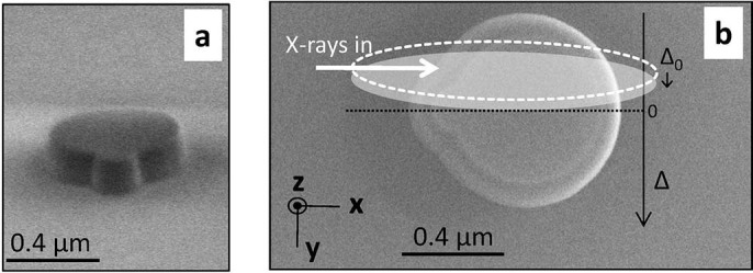
(a) Front view. (b) Same as (a), top view; The direction of the ptychography
translation  (black arrow) and the
scanning step
(black arrow) and the
scanning step  are indicated. The
projected direction of propagation of the incident beam (white arrow)
together with the beam footprint (FWHM of intensity, dotted ellipse) are
shown. The gray ellipse corresponds to the beam footprint at the next
beam-to-sample position. The (
are indicated. The
projected direction of propagation of the incident beam (white arrow)
together with the beam footprint (FWHM of intensity, dotted ellipse) are
shown. The gray ellipse corresponds to the beam footprint at the next
beam-to-sample position. The ( orthogonal laboratory frame is given.
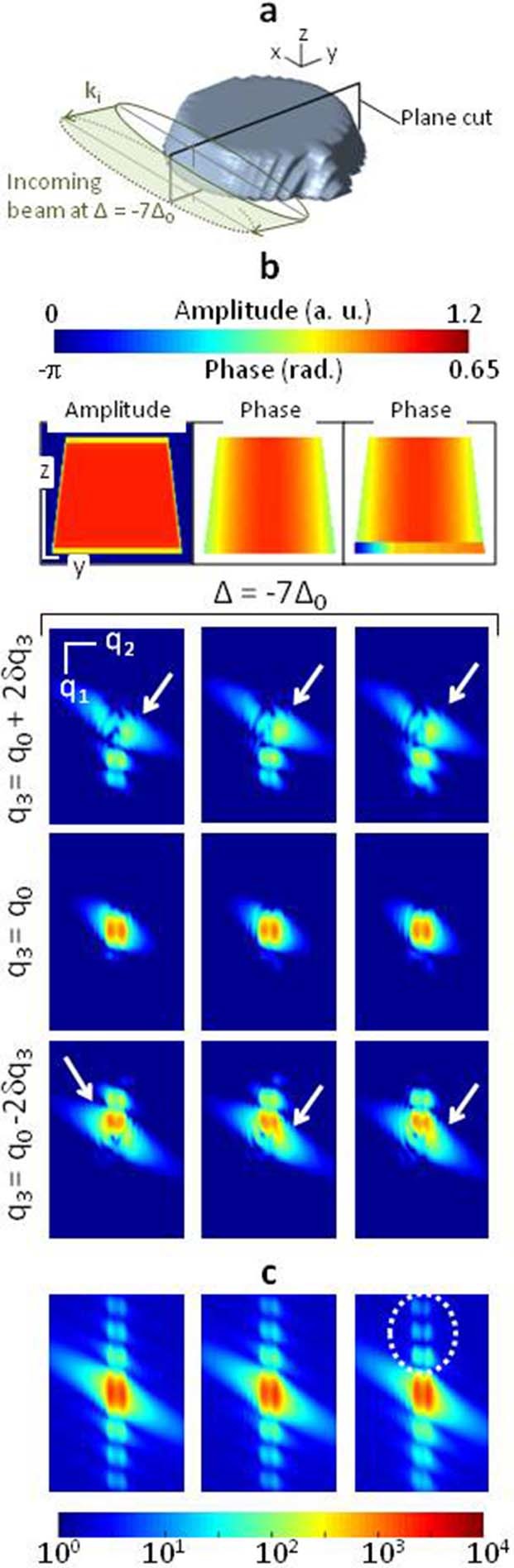
One major parameter of a ptychography experiment is the beam illumination function, whose knowledge is used for the deconvolution operation performed during the ptychography inversion. Although blind deconvolution has been demonstrated for the analysis of 2D ptychography intensity patterns25,26, we observed, for 3D Bragg ptychography, a significant increase of the retrieved image quality when the illumination is known21. This can be intuitively understood by comparing the dimensionality of the problem to solve (the 3D phase of each intensity pattern) to the one of the acquired redundancy, which is only 2D at most (the two possible directions of the beam-to-sample scanning translations). Hence, prior to the 3D x-ray Bragg ptychography experiment itself, a detailed characterization of the profile of the x-ray nano-beam delivered by the synchrotron experimental set-up was performed. The coherent nano-beam was produced by a partially and asymmetrically illuminated focusing lens27. In order to image the complex-valued illumination function at the focal plane, a lens-less microscopy method was used, based on the simple and fast measurement of the over-focused direct beam intensity pattern, i. e., the freely propagated beam far from the focus. This latter was further phased with an error-reduction algorithm28, wherein the wave propagation was performed by the Fresnel propagator. This approach requires the use of a well-defined support in a plane conjugated to the detection one (termed the numerical window), in order to introduce a significant amount of known information (i.e., zero padding) allowing for the algorithm to converge. The ratio between the sizes of the numerical window and the support directly increases with the sampling frequency of the diffraction pattern. In our experimental set-up, this well-defined support constraint was given by the slits defining the lens aperture. Hence, to guarantee that the numerical window located at the slit plane was much larger than the slit aperture (i.e., that the intensity was oversampled), a high-resolution camera, with pixel size typically in the micrometer range, was used (see Methods). Figure 2a shows the over-focused direct beam intensity pattern, where the observation of the high frequency oscillations resulting from the slit truncated beam, demonstrates that the data quality fulfills this oversampling criterion. The resulting retrieved illumination function is shown in Figure 2b (see Methods). The asymmetry in the slit aperture results in an elongated central spot, with size of 0.75 × 0.56μm2 (distance between the two first zeros), along the horizontal and vertical directions, respectively, while the full-width-at-half-maximum (FWHM) of the central spot intensity is 0.31 × 0.23μm2. Beside providing valuable information for our Bragg ptychography experiment, we want to underline the convenience of this nano-beam characterization method, similar to the one presented in Refs. 29,30, which is fast and robust as long as the data oversampling is verified. It permits a high flexibility in the characterization of the beam profile during long-lasting synchrotron experiments.
Figure 2. Experimental considerations for 3D Bragg ptychography: beam profile and Bragg diffraction geometry.
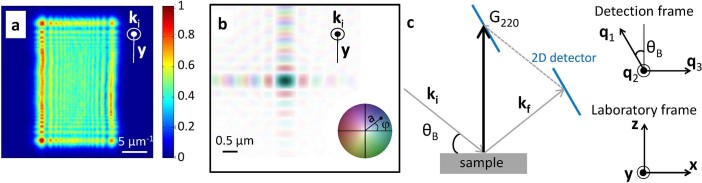
(a) Intensity pattern of the over-focused direct beam (arbitrary units)
measured with a high-resolution camera. (b) Color rendition of the
complex-valued beam profile, retrieved from the inversion of (a) and shown
in the Fresnel zone plate focal plane. The brightness and color correspond
to the linear scale amplitude  and
to the phase
and
to the phase  , respectively. (c)
Description of the 3D Bragg diffraction geometry, including the Bragg angle
(
, respectively. (c)
Description of the 3D Bragg diffraction geometry, including the Bragg angle
( ), the incident and exit wave
vectors (
), the incident and exit wave
vectors ( , respectively) and the
Bragg vector (
, respectively) and the
Bragg vector ( ). The 3D
non-orthogonal (
). The 3D
non-orthogonal ( ) detection frame
is defined in agreement with the detection acquisition modality,
corresponding to the 2D detector plane and to the rocking curve direction.
The (
) detection frame
is defined in agreement with the detection acquisition modality,
corresponding to the 2D detector plane and to the rocking curve direction.
The ( ) laboratory frame is also
shown.
) laboratory frame is also
shown.
The 3D Bragg diffraction ptychography data set was then acquired in the vicinity
of the silicon 220 Bragg reflection (noted G220, with
 m−1),
following the detection scheme shown in Figure 2c. Details
about the acquisition procedure can be found in the Methods section. Due to the
incidence angle
m−1),
following the detection scheme shown in Figure 2c. Details
about the acquisition procedure can be found in the Methods section. Due to the
incidence angle  , the beam footprint
was elongated (1.2 × 0.23μm2, Figure 1b) so that the structure was fully illuminated along
the scattering plane, i. e the plane defined by the incident and exit
wave vectors (
, the beam footprint
was elongated (1.2 × 0.23μm2, Figure 1b) so that the structure was fully illuminated along
the scattering plane, i. e the plane defined by the incident and exit
wave vectors ( , respectively). With
this specific geometry, the whole structure could be investigated by scanning
the beam-to-sample position
, respectively). With
this specific geometry, the whole structure could be investigated by scanning
the beam-to-sample position  along the
axis normal to the scattering plane. The scanning step
along the
axis normal to the scattering plane. The scanning step  was fixed to 50 nm, ensuring enough overlapping
between two successive positions. Typical coherent diffraction patterns acquired
at different
was fixed to 50 nm, ensuring enough overlapping
between two successive positions. Typical coherent diffraction patterns acquired
at different  values and plotted in the
detection frame, that is
(q1,q2,q3) as shown in
Figure 2c and described in Methods, are presented in
Figure 3. Note that the most central position along
q3 is slightly shifted by
values and plotted in the
detection frame, that is
(q1,q2,q3) as shown in
Figure 2c and described in Methods, are presented in
Figure 3. Note that the most central position along
q3 is slightly shifted by  with regards to the origin of the reciprocal space. The continuity
and reproducibility of the different features observed in the diffraction
patterns, further emphasized in the integrated intensity patterns of Figure 3b, are strong evidences of the absence of beam drift
or radiation damage.
with regards to the origin of the reciprocal space. The continuity
and reproducibility of the different features observed in the diffraction
patterns, further emphasized in the integrated intensity patterns of Figure 3b, are strong evidences of the absence of beam drift
or radiation damage.
Figure 3. 3D Bragg ptychography data set.
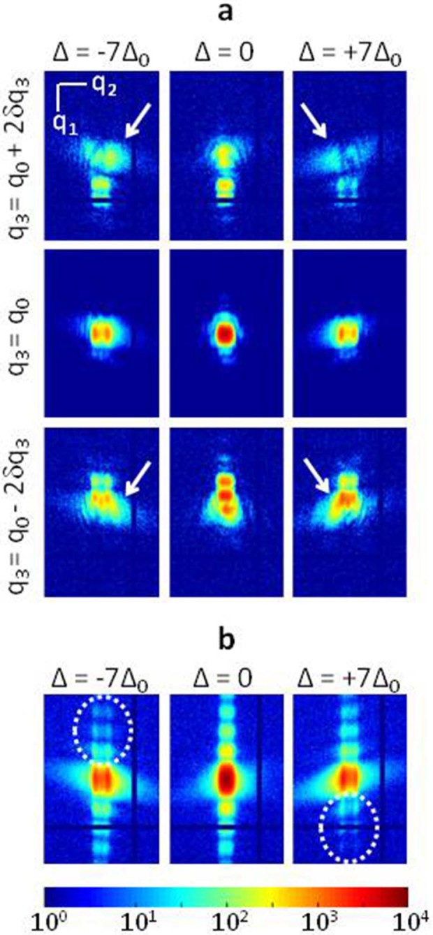
(a) Intensity patterns extracted from the 4D coherent Bragg diffraction
measurements. For each frame, measured in the  plane, only the central part of the pattern is
shown. The steps along
plane, only the central part of the pattern is
shown. The steps along  correspond
to
correspond
to  , relatively to the most central
position
, relatively to the most central
position  while along the
ptychography translation
while along the
ptychography translation  , the
steps are
, the
steps are  (
( m−1 and
  nm). The intensity values in
  have been increased by a factor
of 4 for sake of clarity. The white arrows emphasize the stronger intensity
lobes, which are arising from the structure edges. (b) Intensity integrated
along the
have been increased by a factor
of 4 for sake of clarity. The white arrows emphasize the stronger intensity
lobes, which are arising from the structure edges. (b) Intensity integrated
along the  direction, for a fixed
 , identical to (a). The
dotted ellipses emphasize the missing intensity along the vertical streaks.
In (a) and (b), the vertical and horizontal zero intensity lines correspond
to blind pixels in the detector. The common logarithmic photon scale is
shown in (b).
, identical to (a). The
dotted ellipses emphasize the missing intensity along the vertical streaks.
In (a) and (b), the vertical and horizontal zero intensity lines correspond
to blind pixels in the detector. The common logarithmic photon scale is
shown in (b).
Analysis of the 3D data set
Before we present the result of the ptychographic reconstruction, we show in the
following the detailed analysis of the intensity data set. In addition to
allowing for the estimation of the data quality, the detailed observation of the
intensity data set brings valuable information on the sample crystalline
properties. In particular the presence of a displacement field in a crystal is
directly revealed by its Bragg diffraction pattern. This relies on a simple
property of the Fourier transform, which is well adapted to describe the
propagation of the scattered wave from the sample plane to the far-field
detector. Fourier transforming a purely real function leads to a
centro-symmetric intensity pattern. This situation corresponds to the
strain-free crystal case9. On the contrary, when an arbitrary
displacement field is present in the crystal, it can be modeled by a phase field
in the sample (complex-valued) scattering contrast31. This
imaginary component breaks the centro-symmetry of the diffraction pattern, with
regards to  9.
9.
This kind of behavior is observed in our data set. It is becoming more obvious
when the beam is moving away from the central position, that is when one of the
edges of the structure is strongly illuminated. This is shown in Figure 3a for  . For
. For  , the strongest intensity lobe,
emphasized by the white arrows and arising from the presence of the inclined
edges, is observed for
, the strongest intensity lobe,
emphasized by the white arrows and arising from the presence of the inclined
edges, is observed for  , for all
  values. This corresponds to the
situation where the centro-symetry of the 3D intensity pattern is broken with
regards to the center of the Bragg peak (
values. This corresponds to the
situation where the centro-symetry of the 3D intensity pattern is broken with
regards to the center of the Bragg peak ( ). A similar situation is observed for
  . However, the fact that the intense lobe is
observed for
. However, the fact that the intense lobe is
observed for  (and not
  ) is the signature of a phase field of
opposite sign with regards to the
) is the signature of a phase field of
opposite sign with regards to the  case. On the contrary, when the central part of the structure is illuminated (
 ), the most intense lobe is appearing
on opposite sides of the diffraction pattern for
), the most intense lobe is appearing
on opposite sides of the diffraction pattern for  increasing from negative to positive, a situation
closer to the strain-free case. This whole behavior (centro-symmetry for the
central illumination position and break of centro-symmetry with opposite
behaviors at the edge illumination positions) argues in favor of the presence of
a displacement field at the edge of the silicon structure. Finally, possible
refractions effects have been estimated and found to be negligible in the SOI
structure32.
increasing from negative to positive, a situation
closer to the strain-free case. This whole behavior (centro-symmetry for the
central illumination position and break of centro-symmetry with opposite
behaviors at the edge illumination positions) argues in favor of the presence of
a displacement field at the edge of the silicon structure. Finally, possible
refractions effects have been estimated and found to be negligible in the SOI
structure32.
A second specific behavior is evidenced on the plots of the intensity patterns
that were obtained after integration along  at each fixed
  . They are
shown in Figure 3b for the same
. They are
shown in Figure 3b for the same  s as previously selected. At
  , the vertical streak along
  , corresponding to the thickness interference
fringes, presents a symmetric distribution with regards to
, corresponding to the thickness interference
fringes, presents a symmetric distribution with regards to  . This symmetry is broken at other beam to sample
position. In
. This symmetry is broken at other beam to sample
position. In  , the streak is weaker for
 (dotted ellipse in Figure 3b). This behavior is specific to the presence of a
displacement field along the sample thickness. The fact that the opposite
situation is observed for
(dotted ellipse in Figure 3b). This behavior is specific to the presence of a
displacement field along the sample thickness. The fact that the opposite
situation is observed for  shows that
this displacement is not constant along the translation direction.
shows that
this displacement is not constant along the translation direction.
Numerical simulations were performed in addition to the previous data analysis in
order to evaluate qualitatively which displacement is producing a visible
signature in the intensity data-set. This is particularly relevant when dealing
with limited signal to noise ratio intensities. In the following, the expected
Bragg intensities calculated for different empirical crystalline strain states
and using numerical parameters as close as possible to the experimental
conditions (sample shape and size, illumination function, sampling) are
analyzed. The diffraction patterns shown for  and plotted at reciprocal space coordinates identical to the ones
used in Figure 3 are presented in Figure
4, for an intensity dynamical range comparable to the experimental
data one. Three sample models have been chosen, with the same 3D shape and
density, shown in Figure 4a. In Fig
4b and c, the strain-free case is first
presented on the left column. The average intensity distribution
reproduces fairly the experimental data. One notes that the edge streak is more
inclined than the experimental one, showing a slight discrepancy between the
edge inclinations in the model and in the silicon structure. More interestingly,
the more intense lobe is appearing on opposite sides of the diffraction pattern
when
and plotted at reciprocal space coordinates identical to the ones
used in Figure 3 are presented in Figure
4, for an intensity dynamical range comparable to the experimental
data one. Three sample models have been chosen, with the same 3D shape and
density, shown in Figure 4a. In Fig
4b and c, the strain-free case is first
presented on the left column. The average intensity distribution
reproduces fairly the experimental data. One notes that the edge streak is more
inclined than the experimental one, showing a slight discrepancy between the
edge inclinations in the model and in the silicon structure. More interestingly,
the more intense lobe is appearing on opposite sides of the diffraction pattern
when  increases from negative to
positive, as expected for a centro-symmetric diffraction pattern produced by a
strain-free crystal. The vertical streak evidenced in the integrated intensity
pattern of Figure 4c is equally distributed along
q1. The middle column corresponds to the
introduction of a displacement field developing at the edges of the structure.
This leads to a break of the centro-symmetry, resulting in intensity lobes
behaving similarly to the ones experimentally observed. However, the vertical
streak visible in the integrated intensity plot of Figure
4c is still symmetric. The final introduction of an additional
displacement at the interface (right column) breaks this symmetry along
the thickness streak, leading to the definitive modification of the diffraction
pattern, in good qualitative agreement with the experiment. It demonstrates that
these simultaneous displacement fields at the edges and at the interface
of the structure result to clear and observable signatures in the experimentally
accessible data set. Reciprocally, the experimentally observed diffraction
patterns could be explained by these displacement fields.
increases from negative to
positive, as expected for a centro-symmetric diffraction pattern produced by a
strain-free crystal. The vertical streak evidenced in the integrated intensity
pattern of Figure 4c is equally distributed along
q1. The middle column corresponds to the
introduction of a displacement field developing at the edges of the structure.
This leads to a break of the centro-symmetry, resulting in intensity lobes
behaving similarly to the ones experimentally observed. However, the vertical
streak visible in the integrated intensity plot of Figure
4c is still symmetric. The final introduction of an additional
displacement at the interface (right column) breaks this symmetry along
the thickness streak, leading to the definitive modification of the diffraction
pattern, in good qualitative agreement with the experiment. It demonstrates that
these simultaneous displacement fields at the edges and at the interface
of the structure result to clear and observable signatures in the experimentally
accessible data set. Reciprocally, the experimentally observed diffraction
patterns could be explained by these displacement fields.
Figure 4. Presence of a crystalline displacement field: numerical studies.
Estimation of the expected diffraction patterns calculated for different 3D
strained crystals with shape similar to the SOI structure. (a) Common 3D
iso-surface rendering of the synthetic object together with the incoming
beam shape (FWHM of intensity) for  . The laboratory frame is given; the length of the black lines is
100 nm. (b) Three synthetic models, corresponding to three different strain
states and their corresponding diffraction patterns. The 2D sample
description is shown in the plane indicated in (a) while the diffraction
patterns are taken at the same
. The laboratory frame is given; the length of the black lines is
100 nm. (b) Three synthetic models, corresponding to three different strain
states and their corresponding diffraction patterns. The 2D sample
description is shown in the plane indicated in (a) while the diffraction
patterns are taken at the same  and
and  values as the ones of (Figure 2, left column). (c) Intensity integrated along
the
values as the ones of (Figure 2, left column). (c) Intensity integrated along
the  direction, for the same
  value. The specific features of
the calculated diffraction patterns are emphasized by the white arrows and
the dotted ellipse. The three strain states are as followed: (Left)
The 3D strain-free crystal case. A 2D cut through the 3D amplitude is shown
in (a). Note the assymetry in the spatial scale, which is underlined by the
white lines, representing a 100 nm length. (Middle) Same calculation,
obtained for a strained crystal: a displacement field with a radial symmetry
is introduced at the edge of the structure. A 2D cut through the
corresponding sample phase is shown at the top. (Right) Same as
before with the simultaneous introduction of the displacement field at the
edges and at the interface. This last model produces diffraction patterns in
good agreement with the experimental ones.
value. The specific features of
the calculated diffraction patterns are emphasized by the white arrows and
the dotted ellipse. The three strain states are as followed: (Left)
The 3D strain-free crystal case. A 2D cut through the 3D amplitude is shown
in (a). Note the assymetry in the spatial scale, which is underlined by the
white lines, representing a 100 nm length. (Middle) Same calculation,
obtained for a strained crystal: a displacement field with a radial symmetry
is introduced at the edge of the structure. A 2D cut through the
corresponding sample phase is shown at the top. (Right) Same as
before with the simultaneous introduction of the displacement field at the
edges and at the interface. This last model produces diffraction patterns in
good agreement with the experimental ones.
This preliminary experimental data analysis finally allows to provide a relevant structural model, which is most likely representative of the structural features present in the SOI sample. Therefore, the optimization of the inversion procedure, which is presented in the following, is based on numerical tests performed on this very same structural model which is now the object to retrieve.
3D phase retrieval
Before the inversion of the experimental data set is performed, the inversion procedure needs to be optimized and quantified to ensure the pertinence of the retrieved image and its physical interpretation. Indeed, any inversion process brings its own artifacts due to the presence of photon shot noise33. Understanding these effects requires a detailed analysis which allows to ensure that the best solution is found and permits to avoid over-interpretation of the retrieved image. Using the conclusion of the numerical simulation, different inversion procedures have been tested on an intensity data set produced by the third sample model of Figure 4, further described in Figure 5 (left column). Before inversion, the complete set of diffraction intensity patterns, calculated in the detection frame, was further corrupted by Poisson shot noise in order to take into account the limited amount of photons in the experiment.
Figure 5. Optimizing the inversion scheme.

(Left) The 3D synthetic model object used to test the inversion procedure. It corresponds to the model shown on the right column of Figure 4. (Second column) Retrieved image using a conjugate gradient optimization of the Bouman and Sauer maximum likelihood, initialized with the shape of the object. (Third column) Same as before introducing an additional regularization term to constrain the sample support. (Right) Same as before, initialized with the true synthetic object. The top, middle and bottom rows are different cuts of the 3D object, as defined on the 3D isosurface plot rendition on the right. The assymetric spatial scale is given on left (y,z) and (x,y) cuts. Each line corresponds to a 100 nm length. The sample density and the displacement field color scales are indicated on the right. The excellent agreement observed between the two last retrieved solutions shows that the found inversion process is optimum.
The inversion of the 4D intensity data was performed by optimizing the approximation of the Poissonian likelihood proposed by Bouman and Sauer in Ref. [34] (see also Ref. [33] for details). This was done with a conjugate gradient algorithm chosen for its fast convergence property. The initial estimate was given by the shape of the synthetic model object (the phase was set to zero). Although the reconstruction shown in Figure 5 (second column) allows to recognize the sample structure, the image is clearly degraded, particularly with respect to the phase exact value in the vicinity of the edges. The obtained solution, which is of poor quality only, is therefore not acceptable for our purpose and calls for an improved inversion scheme. The next inversion corresponds to the same inversion process where an additional regularization has been introduced in order to bring reasonable physical information about the sample21. Here we choose to consider the thickness of the sample: the solution we are seeking at is contained only into a film-like support. Due to the limited number of photons resulting in an expected spreading of the object induced by resolution effects, the thickness of the film has to be slightly larger (10 %) than the true object thickness. As can be seen in Figure 5 (third column), this process increases clearly the quality of the reconstruction, which can be hardly distinguished from the synthetic model object, validating the capability of Bragg ptychography to retrieve with a high fidelity the displacement field. A final test is performed to further quantify the solution quality. The same inversion process is used with an initialization given by the synthetic model object. Indeed in this case, the only remaining discrepancies between the solution and the model are expected to result from the presence of shot noise in the data set: shot noise corrupted data are naturally producing a band-limited image of the sample and this latter is inevitably corrupted by the inversion procedure itself and its capability to deal with shot noise (i.e. the noise model). As can be seen on the right column of Figure 5, the retrieved solution in this last test is in excellent agreement with the solution obtained in the previous test. It confirms that the inversion process is optimum. Moreover, it gives a upper limit of the image quality expected for the experimental data. Based on this result, we used this last inversion process to phase back the experimental data set, without assumption on the strain state of the sample.
The whole set of experimental 3D intensity patterns is now analyzed with the optimized 3D Bragg ptychography algorithm (see Methods). The initial guess is the strain-free model object with external shape close to the SOI pattern nominal shape. The result of the reconstruction, plotted in the orthogonal laboratory frame is shown in Figure 6. As can be seen, the external shape is retrieved with a good agreement with the nominal object shape depicted by scanning electron microscopy (Figure 6a,b and Figure 1). The internal density is rather homogeneous (Figure 6c). Some internal fluctuations remain, related most likely to experimental imperfections (e.g., positioning accuracy). Note as well the presence of a bit of aliasing in the data set, which results in a slight truncation of the object along its longer dimension. This could have been easily overcome with the approach developed in Ref. [21] and does not represent an intrinsic limit of the method. The 3D plot allows finally to quantify the resolution, using the presence of sharp edges along the three direct space directions. The resolution voxel size is estimated to about 50 × 45 × 15 nm3 along the x, y and z directions, respectively.
Figure 6. 3D x-ray Bragg ptychography image of the SOI structure.

(a) 3D Isosurface plot rendition of the retrieved crystalline SOI structure
density, shown in the laboratory frame (threshold at 30%). The length of the
frame black lines corresponds to 0.1 μm. (b) Same as (a),
other view. (c) Orthogonal 2D cuts of the density. (d) Orthogonal 2D cuts of
the displacement field component  . The color scale used to plot the
  images is given at the bottom. (e) 2D cut in
the (y,z) plane extracted from (d). The specific behavior of
images is given at the bottom. (e) 2D cut in
the (y,z) plane extracted from (d). The specific behavior of
 is emphasized in the 1D cuts
taken along the colored lines in (f) and (g).
is emphasized in the 1D cuts
taken along the colored lines in (f) and (g).
More interestingly, 3D Bragg ptychography gives access to the phase  of the retrieved complex-valued quantity.
This quantity holds in principle information about the crystalline properties of
the lithographic structure and more precisely about the displacement field
of the retrieved complex-valued quantity.
This quantity holds in principle information about the crystalline properties of
the lithographic structure and more precisely about the displacement field  since31
 |
where  is the direct space coordinate. Hence, the
projection of the displacement
is the direct space coordinate. Hence, the
projection of the displacement  can be
extracted from the phase map using
can be
extracted from the phase map using 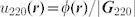 .
This is shown in Figures 6d and 6e.
As expected from the raw data analysis and from the numerical simulations
introducing strain, the measured displacement field exhibits visible variations
at the edges of the structure and at the interface (emphasized in Figure 6f and 6g). This definitively confirms
the capability of x-ray Bragg ptychography experiments to provide high fidelity
images of displacement fields in 3D.
.
This is shown in Figures 6d and 6e.
As expected from the raw data analysis and from the numerical simulations
introducing strain, the measured displacement field exhibits visible variations
at the edges of the structure and at the interface (emphasized in Figure 6f and 6g). This definitively confirms
the capability of x-ray Bragg ptychography experiments to provide high fidelity
images of displacement fields in 3D.
Discussion
The aim of this work was to demonstrate that 3D Bragg ptychography is a microscopy technique able at imaging with strong accuracy the crystalline properties of nano-structured crystal and is able thereby to bring valuable information for the understanding of structural properties of complex crystalline nano-architecture. We think that our careful analysis, which includes the detailed investigation of the raw data, the strained crystal numerical simulations and the optimization of the inversion process, brings the decisive arguments to this demonstration.
Exploring the origin of the observed displacement field is out of reach of this work.
A deeper understanding would require additional local structural information.
Transmission electron microscopy (TEM) could provide the desired strain sensitivity
and resolution, but the sample preparation, which requires the thinning down of the
isolated SOI structure is particularly tricky and subjected to the introduction of
relaxations or defects. The investigation of a series of patterned Si structure
prepared from varying lithographic parameters is mandatory to explore the precise
relationship between the crystalline structure and the sample shape, size and
preparation processes. In spite of these difficulties, we can however argue that the
crystalline behavior at the interface is likely related to the fabrication process
of the SOI wafer. A similar interfacial structure was observed in Ref.
[20]. In addition, the investigation of the considered
interface, performed with TEM on the un-patterned SOI wafer, shows as well a strain
field ( ) at the interface (Figure 7). However, the detailed comparison between the TEM and the
x-ray results is vain due to the strong difference in the image resolution. Indeed,
this requires the introduction of the resolution function parameters (resolution
function model, relative position of interface in TEM and x-rays) for which a good
agreement between TEM and x-rays images can always be found. In addition, finite
element models (FEM) were performed in order to bring some insights to the presence
of the displacement field located at the edge of the structure. This calculation is
based on continuum elasticity theory, using the intrinsic properties of the
materials (i.e. the elastic constants) and does not take into account the
preparation history. The fact that the displacement fields could not be reproduced
by FEM is an argument in favor of a lithographically induced strain field at the
edges.
) at the interface (Figure 7). However, the detailed comparison between the TEM and the
x-ray results is vain due to the strong difference in the image resolution. Indeed,
this requires the introduction of the resolution function parameters (resolution
function model, relative position of interface in TEM and x-rays) for which a good
agreement between TEM and x-rays images can always be found. In addition, finite
element models (FEM) were performed in order to bring some insights to the presence
of the displacement field located at the edge of the structure. This calculation is
based on continuum elasticity theory, using the intrinsic properties of the
materials (i.e. the elastic constants) and does not take into account the
preparation history. The fact that the displacement fields could not be reproduced
by FEM is an argument in favor of a lithographically induced strain field at the
edges.
Figure 7. Transmission electron microscopy at the Si/SiO2 interface (a) Transmission electron microscopy image of the Si <110>/SiO2 interface measured on the un-patterned SOI wafer.

The crystallographic directions of the Si layer are indicated. (b) The
  strain component extracted from (a),
in absolute units. The inset shows the mean value of
strain component extracted from (a),
in absolute units. The inset shows the mean value of  as a function of the distance to the
interface, calculated in the region delimited by the black rectangle. An
increase of
as a function of the distance to the
interface, calculated in the region delimited by the black rectangle. An
increase of  is observed near the
interface.
is observed near the
interface.
To conclude, we have shown that an optimized 3D x-ray Bragg ptychography method, including illumination function knowledge and regularized inversion procedure, possesses the capability to provide high fidelity images of strain fields in nanostructured crystals without dedicated sample preparation. These specificities are required for addressing pending problems in a wide variety of physical or biological material science. We expect that this method will generalize together with the development of the forthcoming x-ray sources and instruments.
Methods
Sample preparation
The SOI wafer is composed of a Si top
layer (0.18μm) and SiO2 layer
(0.02μm) on a Si
top
layer (0.18μm) and SiO2 layer
(0.02μm) on a Si substrate. The patterning method involved e-beam lithography and
SF6-based reactive ion etching to produce inclined edges. Due to the
crystallographic orientation difference between the top layer and the substrate,
it was possible to image solely the Si top structure.
substrate. The patterning method involved e-beam lithography and
SF6-based reactive ion etching to produce inclined edges. Due to the
crystallographic orientation difference between the top layer and the substrate,
it was possible to image solely the Si top structure.
Experiment: beam profile determination
The x-ray experiment was performed at the ID13 beamline at ESRF (European
Synchrotron Radiation Source) with a monochromatic beam of wavelength  nm and bandwidth
  . The finite-sized beam spot needed for the
ptychography scan resulted from the focalisation of a fully coherent beam using
a Fresnel zone plate (FZP) with focal length of 0.14m. For this purpose, the FZP
aperture was reduced to 60 × 40 μm2 in
the vertical and horizontal direction, respectively, so that the illumination
area matched the beam transverse coherence lengths. As the FZP central part was
occluded by a beam stop to avoid direct beam contribution, the aperture was
shifted laterally by 60 μm.
. The finite-sized beam spot needed for the
ptychography scan resulted from the focalisation of a fully coherent beam using
a Fresnel zone plate (FZP) with focal length of 0.14m. For this purpose, the FZP
aperture was reduced to 60 × 40 μm2 in
the vertical and horizontal direction, respectively, so that the illumination
area matched the beam transverse coherence lengths. As the FZP central part was
occluded by a beam stop to avoid direct beam contribution, the aperture was
shifted laterally by 60 μm.
The overfocused direct beam measurement was performed with a high-resolution camera (pixel size of about 1.8 μm) located at 1.72 m from the lens focal plane. The intensity pattern is the result of 100 acquisitions of 1s each, where the zero photon background has been subtracted. The inversion of the intensity data is performed as described in Ref. 29, using a rough estimate of the beam profile as a starting guess. Numerical tests introducing photon shot noise show that a solution of relevant quality is obtained even if the support knowledge is known within ±15%.
Experiment: 3D Bragg ptychography acquisition
The sample was mounted vertically onto a three-axis piezo stage, fixed on the top
of an hexapod. The accurate alignment of the sample center of rotation with
regards to the focal plane was ensured by the use of an optical microscope with
a depth of focus of about 1 μm. The sample was rotated to the
Bragg angle  of the 220 reflection (
 ), which resulted in an elongated
focal spot size of 1.2 × 0.23 μm2, as
schematically shown in Figure 1b.
), which resulted in an elongated
focal spot size of 1.2 × 0.23 μm2, as
schematically shown in Figure 1b.
The intensity acquisition was performed with a Maxipix single photon detector
(516 x 516 pixels of 55 μm size), located at 2.25 m from the
sample. At each position of the beam onto the sample, the sample was rotated in
steps of 0.013°, along the rocking curve. This angular sampling
allowed to ensure that the exit field was fully contained into the conjugated
space associated to the detector frame21. The 20 frames were then
stacked in order to provide the full 3D intensity pattern, for a given beam to
sample position. Each intensity pixel was associated to a reciprocal space
vector  , with coordinates
  and
and  . Precisely,
  and
and  are defined along the detector frame,
parallel and perpendicular to the incident plane, respectively, while
are defined along the detector frame,
parallel and perpendicular to the incident plane, respectively, while  corresponds to the direction of the
rocking curve, i.e., is tangent to the 220 Bragg vector.
corresponds to the direction of the
rocking curve, i.e., is tangent to the 220 Bragg vector.
In order to acquire partially redundant information, the sample position  was scanned along y in steps
of 50 nm (Figure 1b), resulting in an overlapping of 78 %.
The total scanning range (21 steps) ensured that the whole structure was
explored. The acquisition time (30 s per frame) led to an intensity maximum of
about 5700 photons/pixel.
was scanned along y in steps
of 50 nm (Figure 1b), resulting in an overlapping of 78 %.
The total scanning range (21 steps) ensured that the whole structure was
explored. The acquisition time (30 s per frame) led to an intensity maximum of
about 5700 photons/pixel.
Inversion of the experimental data set
The inversion of the intensity data set was performed directly in the detector frame in order to keep the truly measured intensity value in each detector pixel. It preserves thereby the statistical properties of the photon shot-noise corrupted signal. Consequently, the conjugated direct space frame into which all the parameters linked to the sample are described is non-orthogonal21. During the inversion procedure, the illumination function was kept fixed. Its 3D distribution was derived from the beam profile estimated in Figure 2, which was considered as constant along the propagation depth into the sample.
The inversion cycle was initialized by the sample starting estimate, a strain-free structure with external shape close to the SOI pattern nominal shape. In addition, in order to avoid the reconstruction of ambiguous solutions due to the lack of diversity along the beam propagation direction, the search of regularized solutions was enforced21, penalizing the reconstruction of the object outside a film-like support (0.2 μm thick). The conjugate gradient algorithm was used for the inversion, together with a Bouman and Sauer description of the shot-noise probability distribution function34,33. This latter was chosen for its capacity to emphasize the low frequency components, leading to smooth solutions. Other noise models were tested, resulting qualitatively to the same results.
Transmission electron microscopy (TEM)
High-resolution TEM observations were obtained on a JEOL 2200FS microscope
equipped with an ultra-high resolution pole piece and working at 200 keV. The  cross-sectional preparations have
been done by mechanical polishing followed by an argon ion beam milling until
the electron transparency (with a low voltage of 2 kV at the end, to limit the
thickness of amorphous layer on the sides of the preparation). Strain mapping
analysis were performed using the geometrical phase analysis (GPA) software (for
more informations see Refs. [35, 36]). The z axis of the
sample (Figure 1) corresponds to the
cross-sectional preparations have
been done by mechanical polishing followed by an argon ion beam milling until
the electron transparency (with a low voltage of 2 kV at the end, to limit the
thickness of amorphous layer on the sides of the preparation). Strain mapping
analysis were performed using the geometrical phase analysis (GPA) software (for
more informations see Refs. [35, 36]). The z axis of the
sample (Figure 1) corresponds to the  direction.
Author Contributions
The research project was designed by VC. The sample was prepared by AT and the TEM experiments were performed by GP. MB prepared the experimental set-up at the synchtrotron and performed the x-ray measurements together with VC. VC analysed the data together with the help of MA. The manuscript was written by VC, PG and MA with the help of all others.
Additional Information
How to cite this article: Chamard, V. et al.Strain in a silicon-on-insulator nanostructure revealed by 3D x-ray Bragg ptychography. Sci. Rep. 5, 9827; doi: 10.1038/srep09827 (2015).
Acknowledgments
We are grateful to L. Capello from SOITEC, who provided the SOI substrate. J. Daillant and C. Chevallard are warmly acknowledged for their help during the synchrotron experiment. J. Stangl and N. Hrauda are warmly acknowledged for fruitful discussions. The ESRF is acknowledged for allowance of beamtime and the use of the ESRF source. This work is funded by the French ANR under project number ANR-11-BS10-0005.
References
- Bedell S. W., Khakifirooz A., and Sadana D. K. Strain scaling for CMOS. MRS Bulletin 39, 131–137, 2 (2014). [Google Scholar]
- Roberts M. M., et al. Elastically relaxed free-standing strained-silicon nanomembranes. Nat. Mater. 5, 388–393, 2006. [DOI] [PubMed] [Google Scholar]
- Liu J., Sun X., Camacho-Aguilera R., Kimerling L. C., and Michel J. Ge-on-Si laser operating at room temperature. Opt. Lett. 35, 679–681, 2010. [DOI] [PubMed] [Google Scholar]
- Suess M. J., et al. Analysis of enhanced light emission from highly strained germanium microbridges. Nat. Phot. 7, 466 (2013). [Google Scholar]
- Celler G. K., and Cristoloveanu S. Frontiers of silicon-on-insulator. J. Appl. Phys. 93, 4955 (2003). [Google Scholar]
- Xiong G., et al. Elastic relaxation in an ultrathin strained silicon-on-insulator structure. Appl. Phys. Lett. 99, 114103 (2011). [Google Scholar]
- Hÿtch M., Houdellier F., Hüe F., and Snoeck E. Nanoscale holographic interferometry for strain measurements in electronic devices. Nature 453, 1086–1089 (2008). [DOI] [PubMed] [Google Scholar]
- Stangl J., Mocuta C., Chamard V., and Carbone D. Nanobeam X-ray Scattering: Probing matter at the nanoscale. Wiley. (2013). [Google Scholar]
- Newton M. C., Leake S. J., Harder R., and Robinson I. K. Three-dimensional imaging of strain in a single ZnO nanorod. Nat. Mater. 9, 120 (2010). [DOI] [PubMed] [Google Scholar]
- Hoppe W. Beugung im inhomogenen Primrstrahlwellenfeld. Prinzip einer Phasenmessung von Elektronenbeungungsinterferenzen. Acta Crystallograph. A. 25, 495 (1969). [Google Scholar]
- Rodenburg J. M., and Bates R. H. T. The theory of super-resolution electron microscopy via Wigner-distribution deconvolution. Philos. T. Roy. Soc. A 339, 521 (1992). [Google Scholar]
- Faulkner H. M. L., and Rodenburg J. M. Movable aperture lensless transmission microscopy: A novel phase retrieval algorithm. Phys. Rev. Lett. 93, 023903 (2004). [DOI] [PubMed] [Google Scholar]
- Diaz A., et al. Quantitative x-ray phase nanotomography. Phys. Rev. B 85, 020104 (2012). [Google Scholar]
- Chamard V., et al. Three-dimensional x-ray Fourier transform holography: the Bragg case. Phys. Rev. Lett. 104, 165501 (2010). [DOI] [PubMed] [Google Scholar]
- Rodenburg J. M., et al. Hard-x-ray lensless imaging of extended objects. Phys. Rev. Lett. 98, 034801 (2007). [DOI] [PubMed] [Google Scholar]
- Dierolf M., et al. Ptychographic X-ray computed tomography at the nanoscale. Nature 467, 436 (2010). [DOI] [PubMed] [Google Scholar]
- Mocuta C., et al. Beyond the ensemble average: X-ray microdiffraction analysis of single SiGe islands. Phys. Rev. B 77, 245425 (2008). [Google Scholar]
- Vine D. J., et al. Simultaneous X-ray fluorescence and ptychographic microscopy of Cyclotella meneghiniana. Opt. Express. 20, 18287 (2012). [DOI] [PubMed] [Google Scholar]
- Godard P., et al. Three-dimensional high-resolution quantitative microscopy of extended crystals. Nat. Commun. 2, 568 (2011). [DOI] [PubMed] [Google Scholar]
- Berenguer F., et al. X-ray lensless microscopy from undersampled diffraction intensities. Phys. Rev. B 88, 144101 (2013). [Google Scholar]
- Huang X., et al. Three-dimensional Bragg coherent diffraction imaging of an extended ZnO crystal. J. Appl. Crystallogr. 45, 778 (2012). [DOI] [PMC free article] [PubMed] [Google Scholar]
- Hruszkewycz S. O., et al. Framework for three-dimensional coherent diffraction imaging by focused beam x-ray Bragg ptychography. Opt. Lett. 36, 2227 (2011). [DOI] [PubMed] [Google Scholar]
- Hruszkewycz S. O., et al. Quantitative nanoscale imaging of lattice distortions in epitaxial semiconductor heterostructures using nanofocused x-ray Bragg projection ptychography. Nanolett. 12, 5148 (2012). [DOI] [PubMed] [Google Scholar]
- Hruszkewycz S. O., et al. Imaging local polarization in ferroelectric thin films by coherent x-ray Bragg projection ptychography. Phys. Rev. Lett. 110, 177601 (2013). [DOI] [PubMed] [Google Scholar]
- Thibault P., et al. High-resolution scanning x-ray diffraction microscopy. Science 321, 379–382 (2008). [DOI] [PubMed] [Google Scholar]
- Maiden A. M., and Rodenburg J. M. An improved ptychographical phase retrieval algorithm for diffractive imaging. Ultramicroscopy 109, 1256 (2009). [DOI] [PubMed] [Google Scholar]
- Schroer C. G., et al. Coherent x-ray diffraction imaging with nanofocused illumination. Phys. Rev. Lett. 101, 090801 (2008). [DOI] [PubMed] [Google Scholar]
- Fienup J. R. Reconstruction of a complex-valued object from the modulus of its Fourier transform using a support constraint. J. Opt. Soc. Am. A 4, 118 (1987). [Google Scholar]
- Quiney H. M., Peele A. G., Cai Z., Paterson D., and Nugent K. A. Diffractive imaging of highly focused x-ray field. Nat. Phys. 2, 101 (2006). [Google Scholar]
- Mastropietro F., et al. Coherent x-ray wavefront reconstruction of a partially illuminated Fresnel zone plate. Opt. Express. 19, 19223 (2011). [DOI] [PubMed] [Google Scholar]
- Takagi S. A dynamical theory of diffraction for a distorded crystal. J. Phys. Soc. Jpn. 26, 1239 (1969). [Google Scholar]
- Harder R., Pfeifer M. A., Williams G. J., Vartaniants I. A., and Robinson I. K. Orientation variation of surface strain. Phys. Rev. B 76, 115425 (2007). [Google Scholar]
- Godard P., Allain M., Chamard V., and Rodenburg J. Noise models for low counting rate coherent diffraction imaging. Opt. Express. 20, 25914 (2012). [DOI] [PubMed] [Google Scholar]
- Bouman C. A., and Sauer K. A unified approach to statistical tomography using coordinate descent optimization. IEEE Trans. Image Process. 5, 480–492 (1996). [DOI] [PubMed] [Google Scholar]
- Ishizuka, K., A dedicated Site for Quantitative Electron Microscopy, date of access 06/01/2015, http://www.hremresearch.com.
- Hytch M. J., Snoeck E., and Kilaas R. Quantitative measurement of displacement and strain fields from HREM micrographs. Ultramicroscopy 74, 131–146 (1998). [Google Scholar]