Abstract
Transfer printing is a method to transfer solid micro/nanoscale materials (herein called ‘inks’) from a substrate where they are generated to a different substrate by utilizing elastomeric stamps. Transfer printing enables the integration of heterogeneous materials to fabricate unexampled structures or functional systems that are found in recent advanced devices such as flexible and stretchable solar cells and LED arrays. While transfer printing exhibits unique features in material assembly capability, the use of adhesive layers or the surface modification such as deposition of self-assembled monolayer (SAM) on substrates for enhancing printing processes hinders its wide adaptation in microassembly of microelectromechanical system (MEMS) structures and devices. To overcome this shortcoming, we developed an advanced mode of transfer printing which deterministically assembles individual microscale objects solely through controlling surface contact area without any surface alteration. The absence of an adhesive layer or other modification and the subsequent material bonding processes ensure not only mechanical bonding, but also thermal and electrical connection between assembled materials, which further opens various applications in adaptation in building unusual MEMS devices.
Keywords: Physics, Issue 90, Micro-masonry, microassembly, transfer printing, dry adhesives, additive manufacturing, printed processes, microfabrication, inks, microelectromechanical system (MEMS)
Introduction
Microelectromechanical systems (MEMS), such as the miniaturization of large scale ordinary 3D machines, are indispensable for advancing modern technologies by providing performance enhancements and manufacturing cost reduction1,2. However, the current rate of technological advancement in MEMS cannot be maintained without continuous innovations in manufacturing technologies3-6. Common monolithic microfabrication primarily relies on layer-by-layer processes developed for the manufacture of integrated circuits (IC). This method has been quite successful at enabling mass production of high performance MEMS devices. However, owing to its complex layer-by-layer and electrochemically subtractive nature, manufacturing of diversely-shaped 3D MEMS structures and devices, while easy in the macroworld, is very challenging to achieve using this monolithic microfabrication. To enable more flexible 3D microfabrication with less process complexity, we developed a 3D additive micromanufacturing strategy (termed ‘micro/nano-masonry’) which involves a transfer printing-based assembly of micro/nanoscale materials in conjunction with rapid thermal annealing-enabled material bonding techniques.
Transfer printing is a method to transfer solid microscale materials (i.e., ‘solid inks’) from a substrate where they are generated or grown to a different substrate by using controlled dry adhesion of elastomeric stamps. The typical procedure of micro-masonry starts with transfer printing. Prefabricated solid inks are transfer printed using a microtip stamp that is an advanced form of elastomeric stamps and the printed structures are subsequently annealed using rapid thermal annealing (RTA) to enhance ink-ink and ink-substrate adhesion. This manufacturing approach enables the construction of unusual microscale structures and devices that cannot be accommodated using other existing methods7.
Micro-masonry provides several attractive features not present in other methods: (a) the ability to integrate functional and structural solid inks of dissimilar materials to assemble MEMS sensors and actuators all integrated within the 3D structure; (b) the interfaces of assembled solid inks can function as electrical and thermal contacts9,10; (c) the assembly spatial resolution can be high (~1 μm) by utilizing highly-scalable and well-understood lithographic processes for generating solid inks and highly-precise mechanical stages for transfer printing7; and (d) functional and structural solid inks can be integrated on both rigid and flexible substrates in planar or curvilinear geometries.
Protocol
1. Design Masks for Fabrication of Donor Substrate
Design a mask with desired geometry. To fabricate 100 μm x 100 μm square silicon individual units, draw an array of 100 μm x 100 μm squares.
Design a second mask with an identical geometry, with each side extending out an additional 15 μm. For the array of 100 μm x 100 μm squares, draw an array of 130 μm x 130 μm squares that can cover the squares in step 1.1.
Design the anchor geometry. Draw four 20 μm x 40 μm rectangles, each centered along one edge of a square. Place the structures so that the first 15 μm covers the original 100 μm x 100 μm square in step 1.1 and the remaining 25 μm extends outward (as shown in Figure 2). NOTE: Any shape and dimensions can be used as long as the anchor contacts both the patterned material and the substrate. One end of this anchor covers the original geometry in step 1.1 and the other end should extend out the geometry in step 1.2.
2. Prepare Retrievable Donor Substrate
Prepare a p-type doped silicon on insulator (SOI) wafer with 3 μm device layer thickness, with sheet resistance of 1-20 Ω•cm and box oxide layer thickness of 1 μm. NOTE: For various applications these parameters can be altered.
Spin coat photoresist (AZ5214, 3,000 rpm for 30 sec, 1.5 μm thick) and attach the mask designed in step 1.1.
Using a reactive ion etching (RIE) instrument, pattern the device layer of the SOI wafer and remove photoresist mask. After this step, the RIE etched region has exposed the box oxide layer (Figure 2A).
Spin coat photoresist (AZ5214, 3,000 rpm for 30 sec, 1.5 μm thick) and pattern with mask designed in step 1.2.
Heat the wafer at 125 °C for 90 sec on a hot plate.
Immerse the wafer into 49% HF for 50 sec to etch the exposed box oxide layer from step 2.3. After completely drying, remove the masking photoresist (Figure 2B).
Spin coat (AZ5214, 3,000 rpm for 30 sec, 1.5 μm thick) and pattern the anchoring design from step 1.3.
Heat the wafer at 125 °C for 90 sec on a hot plate.
Immerse into 49% HF for 50 min. This step etches the box oxide layer remaining underneath the remaining patterned device layer silicon, resulting in suspended silicon individual units on the photoresist (Figure 2C).
3. Design Masks for a Microtip Stamp
Design a mask with a single 100 μm x 100 μm square.
Design a mask with multiple 12 μm x 12 μm squares inside a 100 μm x 100 μm area.
4. Make the Mold for a Microtip Stamp
Clean a silicon wafer with crystalline orientation of <1-0-0>, deposit 100 nm of silicon nitride using Plasma Enhanced Chemical Vapor Deposition (PECVD) equipment.
Spin coat photoresist (AZ5214, 3,000 rpm for 30 sec, 1.5 μm thick) and pattern with mask designed in step 3.2.
Pattern the silicon nitride layer using 10:1 Buffered Oxide Etchant (BOE).
Dissolve 80 g of potassium hydroxide (KOH) in 170 ml of deionized water and 40 ml of isopropyl alcohol (IPA) mixture a beaker.
Heat the KOH, IPA, and water mixture at 80 °C on a hot plate.
Vertically place the prepared wafer in the beaker with KOH mixture to etch the exposed silicon in crystalline structure (etching rate is around 1 μm/min).
After the exposed silicon is fully etched, remove the wafer from KOH mixture, etch away the silicon nitride using HF, and perform RCA 1 and RCA 2 cleaning (Figure 3A).
Spin coat with SU-8 100 and pattern with the prepared mask from step 3.1 with following recipe: 3,000 rpm for 1 min, soft bake at 65 °C for 10 min and 95 °C for 30 min, expose with 550 mJ/cm2, and post bake at 65 °C for 1 min and 95 °C for 10 min (Figure 3B).
After the SU-8 100 is fully cured, apply a monolayer of (tridecafluoro-1,1,2,3-tetrahydro octyl)-1-trichlorosilane by dropping 3-5 drops of (tridecafluoro-1,1,2,3-tetrahydro octyl)-1-trichlorosilane into a vacuum jar and placing the wafer in the jar and applying the vacuum.
5. Duplicate a Microtip Stamp Using a Mold
Mix polydimethylsiloxane (PDMS) base and curing agent with the ratio of 5:1.
Degas the mixture by placing it in a vacuum jar.
Pour a small portion of the degassed PDMS mixture on the mold and let the PDMS reflow to achieve a flat top surface (Figure 3C).
Place the mold with PDMS in the oven at 70 °C for 2 hr to fully cure the PDMS.
Remove the mold from the oven and peel the PDMS off (Figure 3D).
6. Retrieve Ink from the Donor Substrate and Print on the Target Area
Place the donor substrate onto motorized rotational and x,y-translation stages equipped with a microscope.
Attach the microtip stamp to an independent vertical translational stage.
Under the microscope, align the microtip stamp with the Si ink on the donor substrate using translational and rotational stages. Furthermore, do the tilting alignment between the microtip surface and the Si ink by adjusting a tilting stage. Afterwards, bring the microtip stamp down to make contact.
Slowly bring the microtip stamp down further after initial contact, so that small tips are fully collapsed and the whole surface is in contact with the Si ink on donor substrate.
Quickly raise the z stage, breaking the anchors due to the large contact area between the microtip stamp and the Si ink, to retrieve the Si ink from the donor substrate and attach it to the microtip stamp. NOTE: When the microtip stamp is free of any stress, the compressed microtip restores to its original pyramidal shape, making minimal contact with the retrieved Si ink.
Place the receiver substrate onto an x,y-translation stage and align the retrieved Si ink under the microtip stamp at the desired location.
Descend the z stage until the retrieved Si ink barely makes contact with the receiver substrate.
After making contact, slowly raise the z stage to release the Si ink, printing it on the desired location.
7. Bonding Process
Program a rapid thermal annealing furnace to cycle from RT up to 950 °C in 90 sec, remain at 950 °C for 10 min and cool down to RT (by removing any heat supply in the furnace).
Place the printed receiver substrate in the furnace in an ambient air environment and anneal at 950 °C for 10 min for Si-Si bonding or at 360 °C for 30 min for Si-Au bonding.
Representative Results
Micro-masonry enables heterogeneous material integration to generate MEMS structures that are very challenging or impossible to achieve by monolithic microfabrication processes. In order to demonstrate its capability, a structure (called a ‘micro teapot’) is fabricated solely through micro-masonry. Figure 4A is an optical microscope image of fabricated Si inks on a donor substrate. The designed inks are discs with different dimensions made of single crystalline silicon, which are the building blocks of the micro teapot. Once a donor substrate is independently prepared, discs are transfer printed onto a receiver substrate and annealed layer by layer utilizing a microtip stamp as shown in Figure 4B. The inner region of the micro teapot is hollow as can be seen from each assembled disc. Furthermore, the delicateness of micro-masonry processes is also tested by transfer printing and annealing a rather exquisite photonic crystal platelet (Figures 4C-E). Photonic surfaces are first patterned with nanoimprint lithography and made as transferrable inks on a donor substrate as outlined in the protocol. Once the ink is fully prepared, the photonic crystal platelet is transferred onto four Si rings with 50 μm thickness, forming a table like configuration shown in Figure 4E.
Apart from micro-masonry for silicon inks, images in Figure 5 show examples of micro-masonry adopted to assemble thin Au films. Figure 5A is an optical microscope image of prepared 400 nm thick Au films on a donor substrate. These inks are further processed and tested to transfer print onto a Au surface (Figure 5B), as well as on a Si surface (Figure 5C).
Of key importance with this micro-masonry for Au thin film assembly is that in the absence of any adhesive layer, the transfer printed Au films exhibit electrical conductance with the receiver substrate. While it is difficult to achieve strong mechanical bonding between transfer printed Au films and a receiver Au surface, components are held in place through van der Waal’s force and exhibit great electrical conductance without any further processing (Figure 5B)9.
Conversely, heterogeneous integration of Au thin films with a Si surface is also achieved through transfer printing and rapid thermal annealing at approximately Si-Au eutectic temperature. Through the annealing process, contact resistance at the Si-Au interface is significantly reduced similar to that of sputter deposited sample due to Si-Au eutectic bonding. By transmission line measurement (TLM) experiments, this claim has been substantiated (Figure 5C)10.
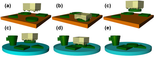 Figure 1. General process flow of micro-masonry7. As a preparation step, a donor substrate, a stamp, and a receiver substrate are independently prepared. (A) Once all of the different components are arranged, first a microtip stamp is attached to a transparent glass slide placed upside down such that the microtips in the stamp are pointing downwards. After the stamp is securely placed, the donor substrate is located on an x,y-axis stage and the stamp is aligned with inks on the donor substrate through a microscope. (B) Subsequently, the stamp is brought down to the donor substrate and a preload is applied on the stamp, such that all microtips in the stamp are fully collapsed. (C) Afterwards, the stamp is quickly raised and the ink is retrieved and attached to a stamp. (D) In order to print the retrieved ink, the stamp with the ink is cautiously aligned to target area and lowered in such that the ink makes contact with the receiver substrate gently while the tips are partially collapsed. (E) While the ink is in contact with the receiver substrate, the stamp is raised slowly. Due to larger van der Waals interaction at ink-receiver interface than at stamp-ink interface, the ink remains on the receiver substrate. (F) The receiver substrate with the assembled inks is moved to a rapid thermal annealing furnace and annealed at 950 °C for 10 min for Si-Si bonding or at 360 °C for Si-Au bonding for 30 min. The annealing step following the transfer printing step completes the micro-masonry procedure. Reproduced with permission from Keum et al.7
Please click here to view a larger version of this figure.
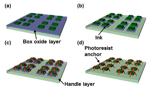 Figure 2. Schematic of donor substrate preparation. (A) On a SOI wafer, the device layer is patterned into desired dimensions and geometry. (B) A following HF wet etching process removes the exposed SiO2 box layer except for the regions beneath the patterned Si. (C) The photoresist is spun and patterned to form anchors. (D) Afterwards, the substrate is submerged into HF to etch away the remaining SiO2. After sufficient time in HF, the array of Si square inks is suspended and free standing with only photoresist anchors on the donor substrate. Please click here to view a larger version of this figure.
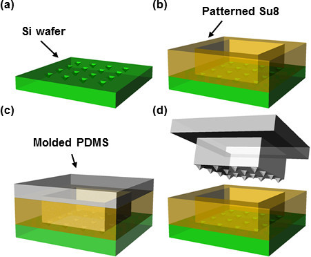 Figure 3. Schematic of stamp fabrication7. (A) In order to make a mold for microtip stamps, a Si wafer is cleaned and small pyramid shaped micropits are created on the wafer through KOH etching. (B) After the etching is done, the surface of the wafer is cleaned through RCA 2 cleaning process followed by applying and patterning SU8 to form a cavity over the microtips. Subsequently, a monolayer of trichlorosilane is coated on the mold to promote the following PDMS molding/demolding process by dropping 3-5 drops of trichlorosilane into a vacuum jar and placing the wafer and vacuuming the vacuum jar. (C) Once the coating is done, the PDMS precursor is poured and cured in the oven. (D) The cured PDMS is simply peeled off from the mold to complete the mold preparation process for a microtip stamp. Reproduced with permission from Keum et al.7
Please click here to view a larger version of this figure.
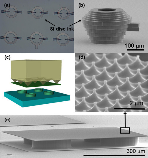 Figure 4. Representative work in Si micro-masonry7. (A) Optical microscope images of ring shape Si inks on a donor substrate, (B) Scanning electron microscope (SEM) image of a micro teapot structure formed by micro-masonry, (C) Illustration of micro-masonry of a silicon photonic surface on four Si rings, (D, E) SEM images of the nanostructures on the photonic surface (D) and the assembled silicon photonic surface on four silicon rings (E). Reproduced with permission from Keum et al.7
Please click here to view a larger version of this figure.
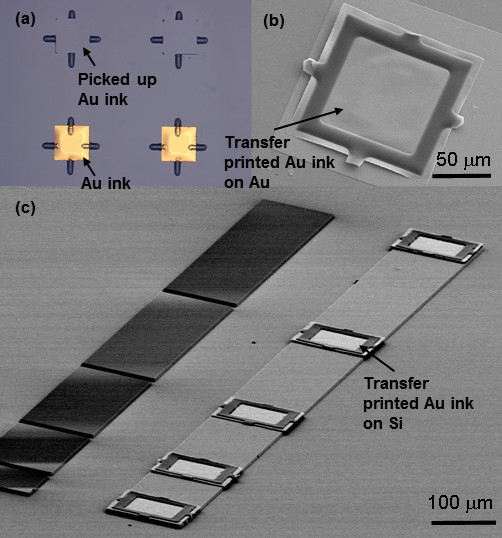 Figure 5. Representative work in Au micro-masonry8. (A) Optical microscopic view of the prepared donor substrate with Au inks retrieved in top row and ready to be retrieved in bottom row, (B) SEM image of a transfer printed Au film on a patterned Au surface, (C) SEM image of transfer printed Au films on a patterned Si strip. Reproduced with permission from Keum et al.8
Please click here to view a larger version of this figure.
Discussion
Micro-masonry, presented in Figure 4, involves silicon fusion bonding in a material bonding step. Silicon fusion bonding is achieved by placing the sample in a rapid thermal annealing furnace (RTA furnace) and heating the sample at 950 °C for 10 min. This annealing condition is both adoptable between Si – Si and Si – SiO2 bonding10,11. Alternatively, the Au bonded with a Si strip as found in Figure 5C adopts eutectic bonding, and therefore, the bonding temperature is around the Si-Au eutectic temperature (363 °C) for 30 min 8. To ensure eutectic bonding, prior to printing Au inks on a Si strip, the Si strip needs to be thoroughly cleansed with 49% HF in order to prevent any impurity such as native oxide at the interface of the Au and Si. Being able to assemble Au films with micro-masonry hugely improves wide adaptation of the micro-masonry manufacturing scheme since it introduces a metal type of material. Due to its low electrical contact resistance with silicon, it can be used as an electrode in the finalized MEMS devices as well as a suspended membrane flexure as presented in Keum et al.9
Transferrable inks developed are currently limited to Si and Au and the materials of their corresponding receiver substrates are Si and SiO2 for Si, and Au and Si for Au. Overall, larger contact area between a receiver substrate and an ink results in ease in the printing step. However, printing an ink while partially contacting the surface is also feasible, resulting in suspended structure, as demonstrated in Figure 4E.
While micro-masonry is a novel approach of microfabrication, there still are limitations to overcome in the process. First and far most is manufacturing scalability since the current deterministic assembly of solid inks is conducted individually rather than at the same time. Also, since the silicon fusion bonding is exercised in high temperature, differences in Si and SiO2 thermal expansion coefficient may result in buckling/delamination in the interface. These limitations need to be further investigated for more broad adaptation of the micro-masonry technique.
As presented in Figure 4, micro-masonry has an immense influence on conventional MEMS processes, which mainly rely on monolithic microfabrication, through its unique additive and flexible manufacturing capability of three dimensional microscale structures that is previously unseen. Furthermore, micro-masonry has the ability to manipulate delicate features in the microscale without damaging the surface because it uses soft elastomeric stamps. Future work includes parallel transfer printing to reduce assembly time, localized bonding processes enabled by laser-assisted annealing, and extending this process to diverse MEMS materials such as SiO2, SixNy, Al, etc.
Disclosures
The authors have nothing to disclose.
Acknowledgments
This work was supported by the NSF (CMMI-1351370).
References
- Stix G. Toward “Point one. Sci Am. Feb. 1995. pp. 90–95.
- Appenzeler T. The Man Who Dared to Think Small. Science. 1991;254:1300–1301. doi: 10.1126/science.254.5036.1300. [DOI] [PubMed] [Google Scholar]
- Madou MJ. Boca Raton, FL: CRC Press; 2002. Fundamentals of Microfabrications The Science of Miniaturization. [Google Scholar]
- Xia Y, Whitesides GM. Soft Lithography. Angew Chem Int Ed. 1998;38:551–575. doi: 10.1002/(SICI)1521-3773(19980316)37:5<550::AID-ANIE550>3.0.CO;2-G. [DOI] [PubMed] [Google Scholar]
- Judy JW. Microelectromechanical systems (MEMS) fabrication, design and applications. Smart Mater Struct. 2001;10:1134–1154. [Google Scholar]
- Jain VK. Micromanufacturing Process. CRC Press; 2012. [Google Scholar]
- Keum H, et al. Silicon micro-masonry using elastomeric stamps for three-dimensional microfabrication. J Micromech Microeng. 2012;22:55018. [Google Scholar]
- Keum H, Chung H, Kim S. Electrical Contact at The Interface between Silicon and Transfer-Printed Gold Films by Eutectic Joining. ACS Appl Mater Interfaces. 2013;5:6061. doi: 10.1021/am4021236. [DOI] [PubMed] [Google Scholar]
- Keum H, Seong M, Sinha S, Kim S. Electrostatically Driven Collapsible Au Thin Films Assembled Using Transfer Printing for Thermal Switching. Appl Phys Lett. 2012;100:211904. [Google Scholar]
- Klaassen EH, et al. Silicon fusion bonding and deep reactive ion etching: a new technology for microstructures. Sens Actuators A. 1996;52:132–139. [Google Scholar]
- Barth PW. Silicon fusion bonding for fabrication of sensors actuators and microstructures. Sens Actuators. 1990;A21 - A23:919–926. [Google Scholar]


