Abstract
Resistive switching effects in transition metal oxide-based devices offer new opportunities for information storage and computing technologies. Although it is known that resistive switching is a defect-driven phenomenon, the precise mechanisms are still poorly understood owing to the difficulty of systematically controlling specific point defects. As a result, obtaining reliable and reproducible devices remains a major challenge for this technology. Here, we demonstrate control of resistive switching based on intentional manipulation of native point defects. Oxide molecular beam epitaxy is used to systematically investigate the effect of Ti/Sr stoichiometry on resistive switching in high-quality Pt/SrTiO3 junctions. We demonstrate resistive switching with improved state retention through the introduction of Ti- and Sr-excess into the near-interface region. More broadly, the results demonstrate the utility of high quality metal/oxide interfaces and explicit control over structural defects to improve control, uniformity, and reproducibility of resistive switching processes. Unintentional interfacial contamination layers, which are present if Schottky contacts are processed at low temperature, can easily dominate the resistive switching characteristics and complicate the interpretation if nonstoichiometry is also present.
Voltage-driven modulation of the electrical resistance of a two-terminal device, commonly referred to as resistive switching, is attractive for next-generation, non-volatile memories, with prospects including very high-density integration and multi-state logic implementation1,2,3,4. A current major roadblock for this technology is the lack of reproducibility and uniformity of the resistive switching effect3,5. This issue is a consequence of the fact that although it is known that resistive switching is caused by point defects6,7,8,9,10,11,12,13,14,15,16, the specific type(s) of defect(s) that are responsible for the switching process are poorly understood. Different types of defects may exist in typical materials that are used for these devices, making it a challenging phenomenon to control and study.
Metal/Nb:SrTiO3 Schottky junctions are a widely investigated materials system for resistive switching7,14,15,17,18,19. They typically exhibit large bipolar switching without the need for an initial forming step. In a previous report20, we demonstrated that the emergence of large resistive switching is governed by the quality of the metal/SrTiO3 interface. Typical metallization processes use polycrystalline metals that are deposited at room temperature. Such interfaces contain interfacial contamination or defect layers that give rise to large switching effects caused by a voltage-induced modulation of the trapped charge in the layer20. The thickness of the interfacial layer determines the voltage drop due to the trapped charge, the degree of Schottky barrier modulation, and thereby the magnitude of the resistive switching effect20. In contrast, high-quality, epitaxial Pt(001) contacts processed at high temperature are (nearly) free of such interface layers but they also do not exhibit resistive switching20. Because interfacial layers associated with low-quality metallization are unintentional and non-uniform, they are unlikely to yield reproducible device performance. Controlled introduction of defects may offer a route towards reproducible and improved switching devices.
Here, we explore this idea by intentionally introducing defects near Pt/Nb:SrTiO3 interfaces. This is accomplished by inserting non-stoichiometric, epitaxial SrTiO3 interlayers, grown by molecular beam epitaxy (MBE), that contain controlled amounts of Ti- or Sr-excess, respectively. We show that such interlayers dramatically alter the switching behavior and significantly improve state retention, compared to devices that rely on the unintentional interface layers discussed above. Furthermore, the results demonstrate the complexity of behavior that is obtained in the presence of both unintentional defect layers and non-stoichiometry, and the need for high quality materials and interfaces to interpret observed resistive switching phenomena.
A key result from ref. 20 is that it establishes a link between voltage-induced resistance modulation and the voltage drop across an interface layer (Δ). The resistance state of the junction is largely determined by the Schottky barrier height (ϕB), which is given by the difference between the metal workfunction (ϕM) and the electron affinity of SrTiO3 (χSTO). As illustrated in Fig. 1, ϕB is modified by Δ:
Figure 1. Band structure of a Schottky junction in the presence of an interface layer.
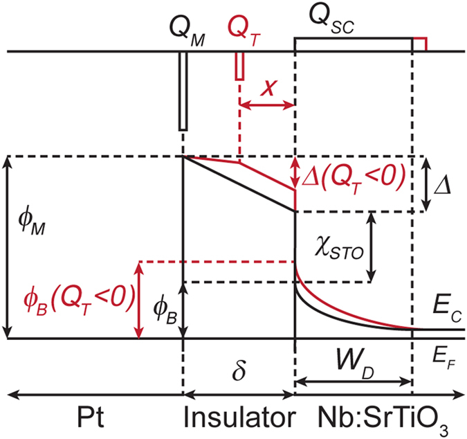
The red lines schematically illustrate the effect of a trapped charge centroid QT present within the interface layer.
 |
A non-zero Δ is a consequence of charge separation between the metal and the doped SrTiO3 and its contribution to Δ is determined by the interface capacitance. The latter is given by the interface layer thickness (δ) and permittivity (εi). A fundamental contribution is that of the space charge in the depletion width of SrTiO3 (WD). Any trapped charge present in the system will also contribute. The contribution of a potentially very complex charge profile can be simplified by considering an equivalent charge centroid (QT), so that Δ can be written as:
 |
where x is the position of QT (as defined in Fig. 1), ND the donor doping level in SrTiO3, q the elementary charge, and ε0 is the vacuum permittivity. This framework was successful in quantifying resistive switching in terms of voltage-induced modulation of trapped charge (ΔQT), which is translated into a modulation of the Schottky barrier height (ΔϕB). Considering only first order effects, Eqs. (1) and (2) give a useful estimate for the magnitude of the resistive switching effect:
 |
The important conclusion for practical devices is the direct dependence of ΔϕB on the interface capacitance (εi/δ). In the case of typical metals deposited at ambient temperatures to form a resistive switching device, εi/δ is dominated by uncontrolled contributions from interface contamination and growth-induced disorder20. This leads to a statistical spread in εi/δ values across different samples and devices, which is directly translated into ΔϕB and the resistive switching performance, negatively affecting device reproducibility.
A key objective of the work presented here was to achieve improved control over the quantities entering Eq. (3). This involves minimizing unintentional contributions to εi/δ by using high quality epitaxial Pt contacts and substituting MBE-grown thin films as dominant interface layers. To intentionally define the amount of trapped charge (and thus ΔQT), we intentionally introduce defects into the near-interface region. Specifically, we investigate A-site off-stoichiometric SrTiO3 as an interface layer. This choice was motivated by the ability to grow epitaxial SrTiO3 layers with a well-studied defect chemistry21,22,23,24,25 on doped SrTiO3 substrates, combined with high-quality epitaxial Pt26. Previous studies on non-stoichiometric SrTiO3 involved polycrystalline films27 and metals28,29. This makes them susceptible to a range of defect-related extrinsic effects, but these studies clearly suggested that resistive switching is sensitive to Ti/Sr stoichiometry.
Results
Structural characterization
SrTiO3 films were grown on Nb:SrTiO3 (001) substrates by hybrid oxide MBE30 with five different Ti/Sr ratios. All films thicknesses were between 20 and 30 nm, chosen to avoid strain relaxation for cation off-stoichiometric SrTiO3 films, which have an expanded lattice parameter21,31. Film lattice parameters and stoichiometries, as determined by high-resolution x-ray diffraction and Rutherford backscattering spectrometry (RBS), respectively, are shown in Fig. 2. As can be seen from Fig. 2(a,b), films grown with a TTIP/Sr flux ratio of 47.8 lie in the middle of the MBE growth window31, within which stoichiometric SrTiO3 films are obtained (Ti/Sr = 1) and the film lattice parameter corresponds to that of the substrate, 3.905 Å [TTIP is titanium tetra isopropoxide used to supply Ti]. Stoichiometric films also exhibit a characteristic c(4 × 4) surface reconstruction32 in in situ reflection high-energy electron diffraction (RHEED), see Fig. 2(b). Ti and Sr-rich films have expanded out-of-plane lattice parameters and RBS indicates that the sample series shown in Fig. 2 spans a wide range of Ti/Sr stoichiometries, between 0.74 and 1.74, see Fig. 2(c). All samples had smooth surfaces, with streaky RHEED patterns and surface roughness <0.2 nm (root mean square values) in atomic force microscopy. Samples were annealed in O2 to eliminate any possible contributions from oxygen vacancies. Cross-section, high-angle annular dark-field (HAADF) scanning transmission electron microscopy (STEM) images of highly off-stoichiometric junctions are shown in Fig. 3. All films are crystalline and epitaxial even in case of very large deviations from stoichiometry. In the Ti-rich regime, locally disordered region are apparent as a change of contrast in the images, suggesting the presence of nanoscale amorphous inclusions of titanium oxide that are typical for Ti-excess films22,23,24. In the Sr-rich regime no extended defects are apparent, which is different from observations in other studies of Sr-rich SrTiO3 films, which exhibit Ruddlesden-Popper (RP) defects21,22,23. This could be due to the higher growth rate (~150 nm/h) in hybrid oxide MBE, which may kinetically limit the condensation of Sr into SrO planes, or the high volatility of the TTIP source, which may facilitate the accommodation of Sr-excess via the formation of Ti vacancies, which is not possible when it is evaporated as Ti metal (which has a sticking coefficient of ~1, see ref. 33). In either case, this suggests that Sr-excess is accommodated by the formation of (randomly distributed) point defects, most likely Ti vacancies, as Sr interstitials have very high formation energies25.
Figure 2. Correlation between lattice parameters, RHEED, and film stoichiometry.
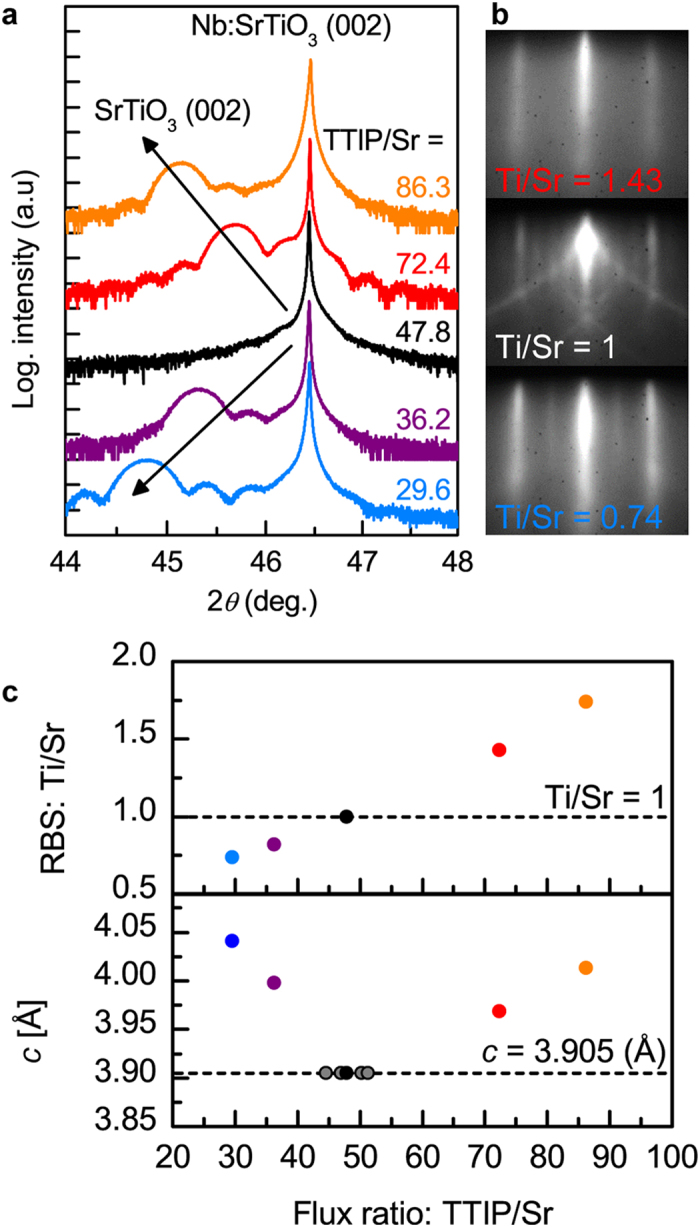
(a) X-ray diffraction spectra of SrTiO3/Nb:SrTiO3 films grown with different stoichiometries. The out-of-plane lattice constant increases for TTIP/Sr flux ratios outside of the MBE growth window. (b) In-situ RHEED patterns along the [110] direction. The streakiness of the patterns indicates smooth film surface and the c(4 × 4) reconstruction for TTIP/Sr = 47.8 is characteristic of stoichiometric growth (Ti/Sr = 1). (c) Ti/Sr stoichiometry determined by RBS and correlation with the out-of-plane lattice constant as a function of flux ratio. The grey dots are homoepitaxial calibration growths of SrTiO3 on SrTiO3 substrates.
Figure 3. STEM images of nonstoichiometric SrTiO3 films.
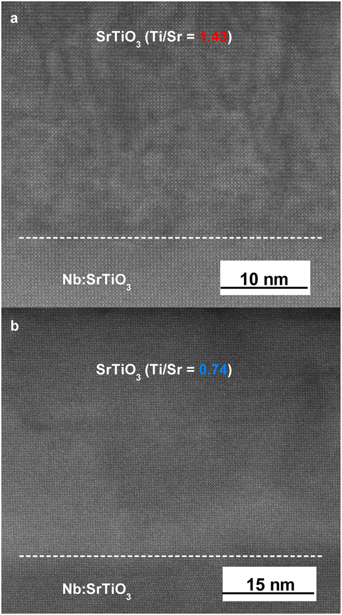
High-angle, annular dark-field scanning transmission electron microscopy cross-section images for (a) Ti-rich and (b) Sr-rich SrTiO3 films.
Current-Voltage Characteristics
Schottky contacts to the SrTiO3/Nb:SrTiO3(001) samples consisted of 100-nm thick Pt, deposited by two different processes. The first used polycrystalline Pt grown by e-beam evaporation at room temperature, which will be referred to as Pt(PC) from here on. The second used epitaxial, Pt(001) grown by DC sputtering at high temperature, as described in ref. 26. Without SrTiO3 interlayers, Pt(PC)/Nb:SrTiO3 junctions show a large current-voltage (I-V) hysteresis due to the presence of an insulating interfacial layer. Both are suppressed in (001)Pt/Nb:SrTiO3 junctions20. A total of ten Pt/SrTiO3 samples were investigated: five different SrTiO3 film stoichiometries and the two types of metallization for each.
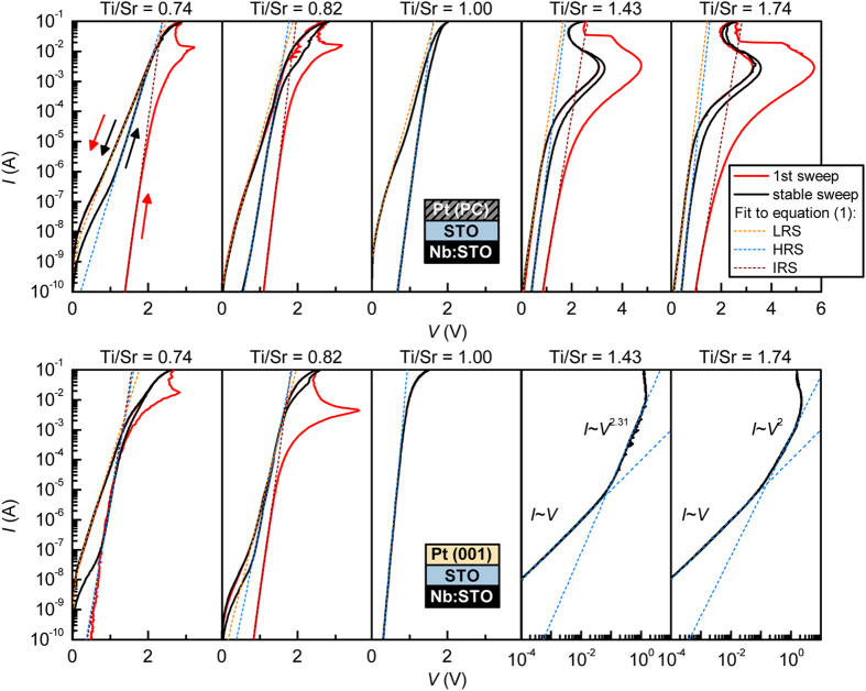
Figure 4 shows the forward bias I-V characteristics of the ten samples. The top and bottom panels show the junctions with Pt(PC) and Pt(001) metallizations, respectively. Horizontally, the panels are ordered according to SrTiO3 interlayer stoichiometry, going from Sr-rich on the left to Ti-rich on the right.
Figure 4. Current-voltage characteristics.
Current-voltage characteristics of all Pt/SrTiO3/Nb:SrTiO3 junctions. Top and bottom rows correspond to junctions with Pt(PC) and Pt(001), respectively. From left to right, the interlayer stoichiometry is tuned from Sr-rich to Ti-rich. If the initial sweep is non-reversible, it is plotted as a red line. Black lines represent stable, reversible sweeps. Dashed lines are thermionic emission fits for IRS, HRS and LRS (initial, high and low resistance states).
As discussed in ref. 20 as well as further below, classic thermionic emission theory provides a good description of the I-V characteristics in most cases:
 |
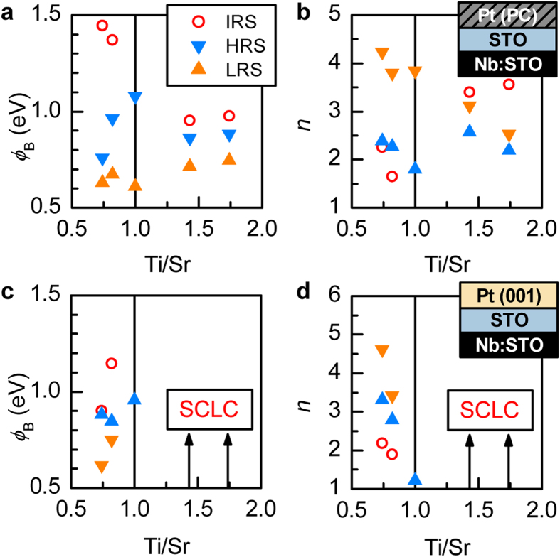
where S, A*, kB and T are the junction area, Richardson constant, Boltzmann constant, and temperature, respectively. The fit parameters are the Schottky barrier height ϕB and the ideality factor, n. Fits to Eq. (1) are shown are shown as dashed lines in Fig. 4. The values obtained for ϕB and n are plotted in Fig. 5 as a function of Ti/Sr stoichiometry in the interlayer.
Figure 5. Schottky barrier properties obtained from I-V fits.
(a,b): Schottky barrier heights ϕB and ideality factors n obtained from fitting the data shown in Fig. 3 for junctions with Pt(PC). (c,d): corresponding results for junctions with Pt(001). SCLC indicates the off-stoichiometry range with space-charge limited conduction.
We first consider the junctions with stoichiometric interlayers (middle panels in both rows). For Pt(PC), a large hysteresis is seen, which is absent for Pt(001). This is similar to the behavior of Pt/Nb:SrTiO3 junctions without interlayers, where the resistive switching effect was shown to originate from unintentional interface layers that are present for Pt(PC) but not for Pt(001)20. Furthermore, the extracted ideality factors of the Schottky barrier in each case are also similar to those reported in ref. 20. This is consistent with charge carriers from Nb:SrTiO3 spreading into the epitaxial SrTiO3 interlayers, as expected in the absence of a conduction band offset. As a result, Pt/Nb:SrTiO3 and Pt/stoichiometric-SrTiO3/Nb:SrTiO3 junctions show very similar characteristics.
The I-V and resistive switching behavior is dramatically altered when the SrTiO3 interlayer is non-stoichiometric. When Pt(PC) is used, both Ti- and Sr-rich junctions go through a non-reversible initial step during which strong negative differential resistance (NDR) effects are seen (solid red lines in Fig. 4, the initial resistance state is labeled IRS). After this initial step, junctions can be cycled repeatedly and reproducibly between high and low resistance states (HRS and LRS), see the solid black lines in Fig. 4. This is reminiscent of the “forming” steps necessary to obtain resistive switching effects in many other materials systems.
The values for ϕB and n change systematically as a function of Ti/Sr ratio, independent of the type of electrode that is used, as shown in Fig. 5. Also evident is a typical trend for these types of junctions, namely that the Schottky barrier is lowered (and n increased) upon switching to LRS. This type of switching, and the effect on the barrier properties, can be attributed to de-trapping of negative charges in the interface layer and/or defects from off-stoichiometry (for quantitative description of this process, see ref. 20).
We note that the effect of the first irreversible step (i.e. the transition from IRS to HRS/LRS) is also described by Eq. (4). This effect is not compatible with an appearance of an Ohmic shunt, i.e. a conductive filament acting as a resistor in parallel with the Schottky barrier, as discussed in refs34,35. Consequently the physics of the first switching step appear to be similar to the stable switching between HRS and LRS via voltage modulation of trapped charge, except for its permanent nature.
The junctions with Pt(PC) have two contributions in the resistive switching effect, namely the unintentional interface layer discussed in ref. 20, and the defects induced by the non-stoichiometric SrTiO3. The junctions with Pt(001) are only controlled by the latter. For Ti-rich interlayers, the use of Pt(001) contacts suppresses the resistive switching effect (see right bottom panels in Fig. 4). Moreover, the conduction mechanism changes from thermionic emission to space-charge limited conduction (SCLC), i.e. the current is bulk-limited instead of interface-limited, yielding a power law dependence of the current on the voltage. This is illustrated by plotting the corresponding data on a log I – log V scale, as was done in Fig. 4. The suppression of switching by high quality contacts shows that the modification of switching behavior in Ti-rich junctions with Pt(PC) contacts [relative to Pt(PC)/stoichiometric-SrTiO3 junctions] originates from an interplay between the defects from the two sources (intentional and unintentional). In contrast, resistive switching in Sr-rich junctions is quite similar for both Pt(001) and Pt(PC) contacts. The magnitude of the effect is reduced for Pt(001), but all four Sr-rich junctions show similar NDR in the first step and I-V characteristics in HRS and LRS with significant excess current over the standard thermionic emission. The latter can be ascribed to tunneling through the Schottky barrier, resulting in an exponential increase that can also be described by Eq. (1) with a very high n ~ 7–10, which is indicative of a field emission process7,36. Again we note that this feature cannot be rationalized as an appearance of a conductive filament acting as a shunt34,35. Instead this is an interface effect, where the defect states near the metal/oxide interface enable electron tunneling through the Schottky barrier.
State Retention Characteristics
Figure 6(a) shows the resistance state retention characteristics of devices with Pt(PC) contacts, which are similar to the Pt/SrTiO3 junctions with low temperature, polycrystalline Pt reported in the literature. Specifically, the HRS is the stable state, while the LRS is transient and decays back to HRS over time after switching. This decay follows a power law dependence (I ~ tβ), associated with charge re-trapping in the interface layer14,20,37. The junction with Pt(PC) and Ti/Sr = 1 shows a fast decay with an exponent β = 0.35. This value is very consistent with our previous study, which found no appreciable change in LRS decay rate with Pt quality20. In contrast, LRS decay rate in both Sr-rich and Ti-rich junctions with Pt(PC) is considerably slower. This is reflected in the decrease of the exponent β to ~ 0.1. Most importantly, for Pt(001)-based junctions with Sr-rich SrTiO3 interlayers that do show resistive switching effects, both HRS and LRS states are stable with time [Fig. 6(b)]. This corresponds to a very small decay exponent (within the noise, β ~ 0).
Figure 6. Resistance state retention characteristics.
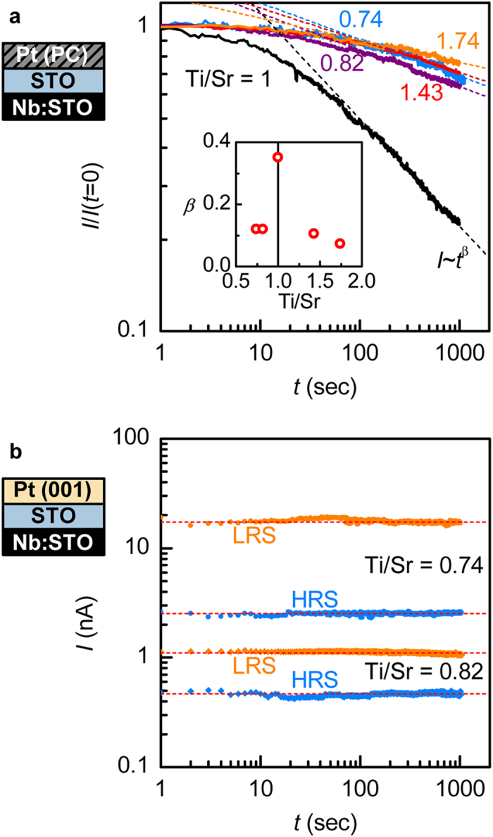
(a) Decay of junction current at V = 0.1 V for LRS with time after switching from HRS, for junction with Pt(PC). Dashed lines are fits to a power law, with its exponent is shown in the inset. (b) State retention for HRS and LRS in Sr-rich junctions with Pt(001).
Discussion
Several conclusions can be drawn from the results shown in Figs 4, 5, 6. First and foremost, the results show that resistive switching with excellent state retention can be achieved by maximizing off-stoichiometry, while concurrently minimizing the unintentional interfacial layer. These conditions are realized for the (001)Pt junctions with Sr-excess SrTiO3 interlayers. The observed trends for β are consistent with an overlap of two contributions to resistive switching: one is associated with Pt(PC) and decays fast (high β); the other one is associated with Ti- or Sr-excess and decays slowly (low β). As mentioned above, the most likely point defects that accommodate Sr-excess are Ti-vacancies, which are deep acceptors25. These defects appear to play a similar beneficial role, in terms of resistance state retention, as Cr dopants, which are also deep acceptors9,10. This is consistent with increased time constants associated with defect levels that are deep within the band gap, leading to a stable resistance state.
Secondly, the study shows that junctions that have similar characteristics as many others reported in the literature [Pt(PC) combined with some degree of nonstoichiometry in the bulk] exhibit switching behavior that is complicated by having two origins, namely the unintentional interface layers, and bulk (near interface) defects. Unintentional contamination layers give rise to volatile resistive switching as was already discussed in ref. 20. The results reported here elucidate the nature of the additional contributions that arise from point defects in the bulk. This includes the appearance of an irreversible, forming-like process, which brings the device from an initial resistance state (IRS) to the first LRS. It appears only in the presence of non-stoichiometry in the SrTiO3. The IRS state is independent of the presence of the unintentional contamination layer, as it also appears in the junctions with Pt(001). The systematic trends in ϕB and n in the IRS as a function of Ti/Sr stoichiometry also establish a close link between the point defects and the IRS state. For all Sr-rich junctions, the IRS is essentially a more extreme version of the HRS (higher ϕB and lower n for IRS), whereas in Ti-rich samples the initially very high n decreases substantially after the forming process.
The logarithmic time dependence that is common to all junctions based on Pt(PC) indicates that the switching mechanism itself is similar, independent of the stoichiometry in the bulk: switching to the LRS corresponds to de-trapping of charges in the unintentional interface layer, the decay of the LRS reflects their re-trapping20. The kinetics of this process is, however, modified by the Ti/Sr stoichiometry (as reflected in β). This points to defect management as a valuable tool for improving state retention performance. This is even more apparent in the junctions with Pt(001) that do not have an unintentional interfacial layer but have a Sr-excess SrTiO3 layer. These junctions show essentially no degradation of either resistance state.
A systematic correlation between nonstoichiometry in the interlayer and the junction characteristics is also apparent in the frequency (f) dependence of the junction capacitance (C) in HRS, shown in Fig. 7(a,b). Except for the expected low frequency deviations in Pt(001)/Ti-rich SrTiO3 junctions (due to the high DC leakage seen in the I-V curves), the capacitive response follows the well-known power law, C~fm-138,39. Figure 7(c) shows the (1-m) as a function to the Ti/Sr ratio. The interpretation of the magnitude of the exponent m in the power law is non-trivial, but generally correlated with defects and the associated relaxation times or hoping probabilities40,41. A helpful framework for its interpretation is the one of random resistor-capacitor networks42,43, within which the power law exponent m and 1-m correspond to the fraction of capacitors and resistors, respectively, in the circuit. A simplistic conclusion is to equate the resistor population (1-m) with defect concentrations, but the trends in Fig. 7(c) are more intricate. For instance, using Pt(001) consistently increases (1-m), which can be interpreted as removal of the capacitor-like unintentional interface layer. It is thus obvious that m cannot be used as a straightforward metric for material quality or defect concentrations, as the Ti/Sr = 1 junction with Pt(001) has a fairly high (1-m) = 0.0072 despite a nearly ideal n of 1.2. The decrease of (1-m) with Ti-excess is likely associated with amorphous Ti regions acting in a capacitor-like fashion when Pt(PC) is used. In contrast, Sr-excess consistently increases (1-m), consistent with it being accommodated in form of randomly distributed point defects that act in a resistor-like manner within the random network picture. The validity of this trend and the close numerical values for both Pt(PC) and Pt(001) cases indicate that it is dominated by the intentional Sr-excess and not the interface layers. This is consistent with the above conclusions on improving state retention behavior (i.e. slowing charge trapping kinetics) by increasing off-stoichiometry and suppressing unintentional interface layers. While the interpretation of dielectric relaxation with frequency is challenging, it is clearly correlated with the types of defects that are relevant for resistive switching. It is thus a useful metric and guide in improving the design of resistive switching junctions.
Figure 7. Dielectric relaxation.

Frequency-dependence of the junction capacitance in IRS for (a) Pt(PC) and (b) Pt(001). Frequency-dependence of the junction capacitance in IRS for (a) Pt(PC) and (b) Pt(001). Dashed lines are fits to C ~ f m-1. The exponent (1-m) values are shown in (c).
Finally, we would like to return to Eq. (3), which estimates the resistive switching effect as ΔϕB ~ ΔQT·δ/εi. The contribution of this work is that it controls both the ΔQT and δ/εi contributions to the resistive switching. The interface capacitance δ/εi is set by using Pt(001), minimizing unintentional defect interface layers, and replacing them with MBE-grown SrTiO3. The trapped charge QT is defined by introducing point defect traps via intentional Ti/Sr off-stoichiometry. Such “clean” material systems offer a route towards reproducible resistive switching. The approach should be fairly general and applicable to other material systems, as it applies to any Schottky junction in presence of trapped charge. As discussed in ref. 20, in the case of Pt/Nb:SrTiO3 junctions, this Schottky barrier height modulation proceeds by standard filling and emptying of trap states, and is inconsistent with ionic electromigration. However, the approach suggested by Eq. (3) should also apply in systems where a trapped charge profile is modified by motion of charged vacancies under an applied voltage.
Additionally, Eq. (3) rationalizes the relatively small magnitude of resistive switching observed in the absence of unintentional interface layers, as seen in Figs 4 and 6(b). In this case, ΔϕB is reduced as the interface layer dielectric constant becomes similar to that of SrTiO3, i.e. on the order of εi = 350. Consequently, much higher ΔϕB could potentially be achieved through improved device design: e.g. substituting the SrTiO3 interlayer for perovskites with lower dielectric constants or by intentionally altering the location of trapped charge (i.e. x in Fig. 1).
In summary, we have shown that the resistive switching characteristics of oxide/metal junctions are highly sensitive to both (i) an interfacial layer and (ii) point defects in the near interface bulk region, each of which contributes in distinguishable ways to the overall phenomenon. Point defects in the oxide layer (e.g. oxygen vacancies44 or deep level dopants like Cr for SrTiO39,10) are widely accepted to be paramount for resistive switching effects. However, unintentional contamination layers that are typically not removed in low temperature metallization can easily overwhelm other contributions and/or interplay with them in non-obvious ways. Isolating the different contributions requires careful design of the junction and high-quality materials. Here we have demonstrated that non-volatile switching can be obtained by inserting Sr-excess SrTiO3 interlayers, while minimizing interface contamination. This makes such junctions an exciting platform for exploring the roles of different defect types in resistive switching effects.
Methods
Film growth and characterization
SrTiO3 films were grown on Nb:SrTiO3(001) substrates by hybrid oxide MBE. Details of the growth procedure and stoichiometry control afforded by this technique are described in detail elsewhere30,31. The film thicknesses were between 20 and 30 nm. All growths were performed at substrate temperature of 900 °C. Layers with five different Ti/Sr ratios were investigated. Lattice parameter measurements using 2θ-ω high resolution X-ray diffraction (XRD) scans (Philips X’PERT Panalytical MRD Pro Thin-Film Diffractometer) and Rutherford backscattering spectrometry (RBS) were used to determine the film stoichiometry. The stoichiometry of each film was determined by Rutherford backscattering (RBS) measurements carried out at Rutgers University and analyzed using the SIMNRA program.
Device Fabrication and Measurement
Devices were fabricated by depositing 100-nm thick Pt on stoichiometric or nonstoichiometric SrTiO3 films, respectively. Polycrystalline Pt films [Pt(PC)] were grown by e-beam evaporation at room temperature. Epitaxial, Pt(001) was grown by DC sputtering at 825 °C26. Square-shaped 45 × 45 μm2 top electrodes were patterned by standard photolithography and wet etching of Pt in aqua regia at 60 °C20,45. A 30-sec anneal in oxygen at 800 °C was performed to eliminate possible contribution from oxygen vacancies. Ohmic contacts to the Nb:SrTiO3 substrate consisted of Au(300 nm)/Ni(20 nm)/Al(40 nm) deposited by electron beam evaporation. I-V characteristics were measured using needle probes and a HP 4155 Semiconductor Parameter Analyzer. Forward bias measurement (switching from HRS or IRS to LRS) were performed in current-controlled mode, ramping from 1 pA to 100 mA and back. Reverse bias sweeps were performed in voltage controlled mode, ramping from zero to a value between -3 and -7 V and back, calibrated to reproducibly revert from LRS to HRS.
Additional Information
How to cite this article: Mikheev, E. et al. Tailoring resistive switching in Pt/SrTiO3 junctions by stoichiometry control. Sci. Rep. 5, 11079; doi: 10.1038/srep11079 (2015).
Acknowledgments
This work was supported by the Air Force Office of Scientific Research under a MURI grant (grant.-no. FA9550-12-1-0038). E.M. and A.J.H. were also partially supported by the FAME Center, one of six centers of STARnet, a Semiconductor Research Corporation program sponsored by MARCO and DARPA. A.J.H. acknowledges support through an Elings Prize Fellowship of the California Nanosystems Institute at University of California, Santa Barbara. The work made use of the UCSB Nanofabrication Facility, a part of the NSF-funded NNIN network. A.P.K. was supported by the UCSB MRL, which is supported by the MRSEC Program of the U.S. National Science Foundation under Award No. DMR-1121053 and by the U.S. National Science Foundation through a Graduate Research Fellowship (Grant no. DGE-1144085).
Footnotes
Author Contributions E.M. and A.P.K. performed the MBE growth. E.M. carried out the device fabrication and analyzed the electrical data. TEM studies were done by J.H. and the analysis of the RBS by A.J.H., E.M. and S.S. wrote the manuscript.
References
- Sawa A. Resistive switching in transition metal oxides. Mater. Today 11, 28–36 (2008). [Google Scholar]
- Waser R. & Aono M. Nanoionics-based resistive switching memories. Nat. Mater. 6, 833–840 (2007). [DOI] [PubMed] [Google Scholar]
- Yang J. J. S., Strukov D. B. & Stewart D. R. Memristive devices for computing. Nat. Nanotechnol. 8, 13–24 (2013). [DOI] [PubMed] [Google Scholar]
- Zhirnov V. V., Meade R., Cavin R. K. & Sandhu G. Scaling limits of resistive memories. Nanotechnology 22, 254027 (2011). [DOI] [PubMed] [Google Scholar]
- Wong H. S. P. et al. Metal-Oxide RRAM. Proc. IEEE 100, 1951–1970 (2012). [Google Scholar]
- Rossel C., Meijer G. I., Bremaud D. & Widmer D. Electrical current distribution across a metal-insulator-metal structure during bistable switching. J. Appl. Phys. 90, 2892–2898 (2001). [Google Scholar]
- Fujii T. et al. Electrical properties and colossal electroresistance of heteroepitaxial SrRuO3/SrTi1-xNbxO3 (0.0002<=x<=0.02) Schottky junctions. Phys. Rev. B 75, 165101 (2007). [Google Scholar]
- Karg S. F. et al. Transition-metal-oxide-based resistance-change memories. IBM J. Res. Dev. 52, 481–492 (2008). [Google Scholar]
- Janousch M. et al. Role of oxygen vacancies in Cr-doped SrTiO3 for resistance-change memory. Adv. Mater. 19, 2232 (2007). [Google Scholar]
- Cho S. et al. Effect of Cr concentration on resistance switching in Cr-doped SrZrO3 films and surface accumulation of Cr ions. J. Appl. Phys. 108, 103716 (2010). [Google Scholar]
- Huang J. J., Kuo C. W., Chang W. C. & Hou T. H. Transition of stable rectification to resistive-switching in Ti/TiO2/Pt oxide diode. Appl. Phys. Lett. 96, 262901 (2010). [Google Scholar]
- Lee M. J. et al. A fast, high-endurance and scalable non-volatile memory device made from asymmetric Ta2O5-x/TaO2-x bilayer structures. Nat. Mater. 10, 625–630 (2011). [DOI] [PubMed] [Google Scholar]
- Seo Y., Song M. Y., Park S. & Kim T. G. Analysis of electronic carrier traps in Cr-SrTiO3-based charge trap flash memory devices. Appl. Phys. Lett. 100, 243501 (2012). [Google Scholar]
- Kan D., & Shimakawa Y. Transient behavior in Pt/Nb-doped SrTiO3 Schottky junctions. Appl. Phys. Lett. 103, 142910 (2013). [Google Scholar]
- Rodenbucher C. et al. Cluster-like resistive switching of SrTiO3: Nb surface layers. New J. Phys. 15, 103017 (2013). [Google Scholar]
- Shibuya K., Dittmann R., Mi S. B. & Waser R. Impact of Defect Distribution on Resistive Switching Characteristics of Sr2TiO4 Thin Films. Adv. Mater. 22, 411 (2010). [DOI] [PubMed] [Google Scholar]
- Park C., Seo Y., Jung J., & Kim D. W. Electrode-dependent electrical properties of metal/Nb-doped SrTiO3 junctions. J. Appl. Phys. 103, 054106 (2008). [Google Scholar]
- Li J. Y., Ohashi N., Okushi H., & Haneda H. Temperature dependence of carrier transport and resistance switching in Pt/SrTi1-xNbxO3 Schottky junctions. Phys. Rev. B 83, 125317 (2011). [Google Scholar]
- Wang Y. H. et al. Investigation of the resistance switching in Au/SrTiO3:Nb heterojunctions. Appl. Phys. Lett. 103, 031601 (2013). [Google Scholar]
- Mikheev E., Hoskins B. D., Strukov D. B. & Stemmer S. Resistive switching and its suppression in Pt/Nb:SrTiO3 junctions. Nat. Commun. 5, 3990 (2014). [DOI] [PMC free article] [PubMed] [Google Scholar]
- Ohnishi T., Shibuya K., Yamamoto T. & Lippmaa M. Defects and transport in complex oxide thin films. J. Appl. Phys. 103, 103703 (2008). [Google Scholar]
- Suzuki T., Nishi Y. & Fujimoto M. Defect structure in homoepitaxial non-stoichiometric strontium titanate thin films. Philos. Mag. A 80, 621–637 (2000). [Google Scholar]
- Brooks C. M. et al. Growth of homoepitaxial SrTiO3 thin films by molecular-beam epitaxy. Appl. Phys. Lett. 94, 162905 (2009). [Google Scholar]
- Stemmer S., Streiffer S. K., Browning N. D. & Kingon A. I. Accommodation of nonstoichiometry in (100) fiber-textured (BaxSr1-x)Ti1-yO3+z thin films grown by chemical vapor deposition. Appl. Phys. Lett. 74, 2432–2434 (1999). [Google Scholar]
- Janotti A., Varley J. B., Choi M. & Van de Walle C. G. Vacancies and small polarons in SrTiO3. Phys. Rev. B 90, 085202 (2014). [Google Scholar]
- Son J., Cagnon J. & Stemmer S. Strain relaxation in epitaxial Pt films on (001) SrTiO3. J. Appl. Phys. 106, 043525 (2009). [Google Scholar]
- Aslam N. et al. Impact of composition and crystallization behavior of atomic layer deposited strontium titanate films on the resistive switching of Pt/STO/TiN devices. J. Appl. Phys. 116, 064503 (2014). [Google Scholar]
- Kim Y. S. et al. Impact of vacancy clusters on characteristic resistance change of nonstoichiometric strontium titanate nano-film. Appl. Phys. Lett. 104, 013501 (2014). [Google Scholar]
- Muenstermann R. et al. Correlation between growth kinetics and nanoscale resistive switching properties of SrTiO3 thin films. J. Appl. Phys. 108, 124504 (2010). [Google Scholar]
- Jalan B., Engel-Herbert R., Wright N. J., & Stemmer S. Growth of high-quality SrTiO3 films using a hybrid molecular beam epitaxy approach. J. Vac. Sci. Technol. A 27, 461–464 (2009). [Google Scholar]
- Jalan B., Moetakef P., & Stemmer S. Molecular beam epitaxy of SrTiO3 with a growth window. Appl. Phys. Lett. 95, 032906 (2009). [Google Scholar]
- Kajdos A. P., & Stemmer S. Surface reconstructions in molecular beam epitaxy of SrTiO3. Appl. Phys. Lett. 105, 191901 (2014). [Google Scholar]
- Theis C. D. et al. Adsorption-controlled growth of PbTiO3 by reactive molecular beam epitaxy. Thin Solid Films 325, 107–114 (1998). [Google Scholar]
- Aubry V., & Meyer F. Schottky Diodes with High Series Resistance - Limitations of Forward I-V Methods. Journal of Applied Physics 76, 7973–7984 (1994). [Google Scholar]
- Chattopadhyay P. The effect of shunt resistance on the electrical characteristics of Schottky barrier diodes. Journal of Physics D-Applied Physics 29, 823–829 (1996). [Google Scholar]
- Rhoderick E. H. Metal-Semiconductor Contacts. IEE Proc.-I 129, 1–14 (1982). [Google Scholar]
- Zhang H. J. et al. Effect of oxygen content and superconductivity on the nonvolatile resistive switching in YBa2Cu3O6+x/Nb-doped SrTiO3 heterojunctions. Appl. Phys. Lett. 94, 092111 (2009). [Google Scholar]
- Jonscher A. K. The Universal Dielectric Response and Its Physical Significance. IEEE Trans. Electr. Insul. 27, 407–423 (1992). [Google Scholar]
- Jonscher A. K. Dielectric relaxation in solids. J. Phys. D 32, R57–R70 (1999). [Google Scholar]
- Horikawa T., Makita T., Kuroiwa T. & Mikami N. Dielectric-Relaxation of (Ba,Sr)TiO3 Thin Films. Jpn. J. Appl. Phys. 34, 5478–5482 (1995). [Google Scholar]
- Baniecki J. D. et al. Dielectric relaxation of Ba0.7Sr0.3TiO3 thin films from 1 mHz to 20 GHz. Appl. Phys. Lett. 72, 498–500 (1998). [Google Scholar]
- Almond D. P. & Bowen C. R. Anomalous power law dispersions in ac conductivity and permittivity shown to be characteristics of microstructural electrical networks. Phys. Rev. Lett. 92, 157601 (2004). [DOI] [PubMed] [Google Scholar]
- Panteny S., Stevens R. & Bowen C. R. The frequency dependent permittivity and ac conductivity of random electrical networks. Ferroelectrics 319, 199–208 (2005). [Google Scholar]
- Yang J. J. et al. Memristive switching mechanism for metal/oxide/metal nanodevices. Nat. Nanotechnol. 3, 429–433 (2008). [DOI] [PubMed] [Google Scholar]
- Kollensperger P. A. et al. Patterning of platinum (Pt) thin films by chemical wet etching in Aqua Regia. J. Micromech. Microeng. 22, 067001 (2012). [Google Scholar]


