

Abstract
Compact high-resolution panel detectors using virtual pinhole (VP) PET geometry can be inserted into existing clinical or pre-clinical PET systems to improve regional spatial resolution and sensitivity. Here we describe a compact panel PET detector built using the new Though Silicon Via (TSV) multi-pixel photon counters (MPPC) detector. This insert provides high spatial resolution and good timing performance for multiple bio-medical applications. Because the TSV MPPC design eliminates wire bonding and has a package dimension which is very close to the MPPC’s active area, it is 4-side buttable. The custom designed MPPC array (based on Hamamatsu S12641-PA-50(x)) used in the prototype is composed of 4 × 4 TSV-MPPC cells with a 4.46 mm pitch in both directions. The detector module has 16 × 16 lutetium yttrium oxyorthosilicate (LYSO) crystal array, with each crystal measuring 0.92 × 0.92 × 3 mm3 with 1.0 mm pitch. The outer diameter of the detector block is 16.8 × 16.8 mm2. Thirty-two such blocks will be arranged in a 4 × 8 array with 1 mm gaps to form a panel detector with detection area around 7 cm × 14 cm in the full-size detector. The flood histogram acquired with Ge-68 source showed excellent crystal separation capability with all 256 crystals clearly resolved. The detector module’s mean, standard deviation, minimum (best) and maximum (worst) energy resolution were 10.19%, +/−0.68%, 8.36% and 13.45% FWHM, respectively. The measured coincidence time resolution between the block detector and a fast reference detector (around 200 ps single photon timing resolution) was 0.95 ns. When tested with Siemens Cardinal electronics the performance of the detector blocks remain consistent. These results demonstrate that the TSV-MPPC is a promising photon sensor for use in a flat panel PET insert composed of many high resolution compact detector modules.
Keywords: high resolution, flat panel, PET detector, 4-side buttable MPPC
1. Introduction
1.1. VP-PET systems
High resolution detector inserts with virtual pinhole (VP) PET geometry have been demonstrated effective in improving regional spatial resolution and sensitivity of existing clinical and pre-clinical PET scanners[1]. Dedicated insert devices have been developed by different research groups, e.g. pre-clinical insert device designed in partial or full ring[2][3][4] and the insert device for clinical applications with half-ring geometry[5]. A compact flat panel detector which provides a relatively large detection area offers versatile detector geometry for multi-purpose VP-PET applications. For organ-specific clinical applications, instead of building a dedicated PET scanner, higher resolution imaging applications with improved sensitivity are possible using a flat panel insert device (shown in Figure 1), potential uses include clinical imaging of head and neck, breast, internal mammary nodes, prostate, etc. The simulation study in a Siemens Biograph 64 PET/CT scanner of a silicon detector insert with detection area similar to our flat panel detector shows significant improvement in resolution with hot rods phantom study[6]. Silicon detectors have much lower density than lutetium yttrium oxyorthosilicate (LYSO) based detectors, thus the proposed silicon probe detector was composed of 10 layers to achieve reasonable detection efficiency. This multiple layer detector is read out by complicated electronics and the timing performance (~10 ns coincidence timing resolution) is worse than the scanner detectors (less than 2 ns) based on lutetium oxy-orthosilicate (LSO), so a wide time window would be applied for coincidence events acquisition.
Figure 1.

VP-PET geometry with flat panel insert and the set up used for internal mammary nodes and breast imaging. One flat panel configuration is used for most of the applications. For some applications, like breast imaging, another panel can be added and positioned at around 90° to each other.
In addition to applications in biomedical imaging, PET technology is used in other fields. We recently built a dedicated PET imager for plant sciences [7]. The spatial resolution of our PlantPET is approximately 1.25 to 1.5 mm; this is mainly limited by the upper half-ring which uses bigger crystals with a 2.4 × 2.4 mm2 cross-section. We expect to achieve up to 1 mm resolution with a flat panel insert (shown in Figure 2). Improved resolution is important for imaging small plants like Arabidopsis thaliana, a model plant for genome analysis.
Figure 2.

Geometry configuration of plant PET system with flat panel. The green half-ring detector is composed of detector modules with 1.59 × 1.59 × 10 mm3 crystal pitch size. The flat panel detector is rendered in yellow and its crystal pitch size is 1 × 1 × 3 mm3. The larger, upper half-ring outlined in white lines is composed of bigger crystals with 2.4 × 2.4 × 10 mm3 pitch; this upper ring is turned off when the flat panel detector is used to acquire coincidence data.
1.2. Compact detector module design based on TSV MPPC photon sensors
The previously reported half-ring human insert device is based on position sensitive photon multiplier tube (PS-PMT)[5]. In contrast to these PS-PMTs, solid state photo multipliers (SS-PMT), which are also called as silicon multiplier (SiPM), or multi-pixel photon counters (MPPC) provide advantages including compact physical profile and insensitivity to magnetic fields. For our VP-PET insert applications, MPPC based detectors offer the additional benefit of reduced Compton scatter from the photon sensor’s low-density packaging materials. Several PET systems based on MPPC show excellent performance with respect to small crystal separation capability, good energy and timing resolution[8][9][10][11][12]. VP-PET insert devices are designed to be as compact as possible; this strategy imposes fewer space constraints when placing an insert close to the regions of interest (ROI) for different clinical applications.
The VP-PET insert detector system described here is meant to be integrated into commercial PET scanners to enhance their image resolution. Our current approach dictates the detectors to be compatible with the read-out electronics of commercial PET scanners. The Siemens Biograph 64 clinical PET scanner’s block detector is composed of a 13 × 13 LSO crystal array. Its Cardinal electronics can support up to 16 × 16 crystals per array with a change of its singles event data format. We contracted Siemens Molecular Imaging Inc. to modify its firmware to support this function. For plant PET insert, the scanner uses the Siemens QuickSilver electronics which supports block detectors, each composed of a 20 x 20 LSO crystal array. As a result, the proposed VP-PET flat panel detector module which has 256 crystals per block, can be decoded by the QuickSilver electronics without any additional firmware modification.
In small modular detector design, edge crystals require special consideration because they are a big portion of the total crystal number. The previous generation 3 × 3 mm2 MPPC sensor commonly used for small animal PET systems has 0.5 mm dead space around its sensitive area due to packaging. As a result, a finished MPPC array has an overall dimension much greater than the sensitive area needed for the scintillator array. Complex light guide designs are often used to couple the crystal array and photon sensor with different sizes to regulate the light propagation for edge crystal identification[13][8][14]. Such designs result in good edge crystal separation even for very small crystals, but also bring in some performance degradation. Both energy and timing resolution of edge crystals are worse than center crystals; this is mainly caused by the light loss with the complex light guide structure.
Hamamatsu (Hamamatsu Photonics K.K.) is the first manufacturer to provide a commercially available 4-side buttable MPPC cells with the through surface via (TSV) fabrication technique[15]. The TSV MPPC offers at least two clear advantages beyond traditional edge wire bonding design. First, it shortens the traces between the individual micro-cells and wire bonding pads which greatly reduces the trace-induced parasitic resistance and capacitance; although not studied in this paper, this feature will potentially improve timing performance[16]. Second, with this TSV process, a single cell’s dead space from the four edges is greatly reduced to a minimum of 100 μm. As a result, the MPPC array can have an outer dimension that approaches that of the crystal array; this feature significantly simplifies the light guide design for our proposed compact detector modules. The single TSV MPPC cell performance has been previously reported[15][17]. This paper explores the potential advantage of using the new TSV MPPC in a compact detector module design that maintains a good and uniform performance for all the crystals. Compact detector module design is also vital for flat panel detector to be used for VP-PET insert systems.
2. Material and methods
2.1. System design concept
Our flat panel PET detector is composed of 32 high resolution block detectors arranged in a 4 × 8 array and mounted on a carbon fiber plate. Four detector blocks form a module, which is read out by a 16-channel amplifier board. Signals from the 8 amplifier boards can be read out by either Siemens QuickSilver[18](for small animal and plant PET scanners) or Siemens Cardinal (for clinical PET scanner) electronics. With this 4 × 8 array configuration, the flat panel has an active area of 7 cm × 14 cm. The thickness of the block detector is only 7.5 mm. The targeted dimensions of the entire panel detector will be comparable to a smart phone with a 5-inch screen (amplifier boards will be enclosed in a separated box).
2.2. Detector block
The stacked structure of the compact detector module is shown in Figure3. Each module hosts a 16 × 16 LYSO crystal array with a crystal size of 0.92 × 0.92 × 3 mm3 at 1 mm pitches, giving a 16 mm × 16 mm detection area. The acrylic light guide regulates the light propagation with narrow cuts on four edges to improve identification of corner crystals. The 4-side buttable TSV-MPPC cell is very suitable for compact high-resolution detector block designs. We custom designed a MPPC array with an active area that matches the crystal array’s dimension; this greatly simplifies the light guide design. The resistor network is on a separated printed circuit board (PCB) connected to the MPPC array via a high-density small connector (0.4 mm Razor Beam™ LP Ultra Fine Pitch socket strip and terminal strip, Samtec, Inc.), allowing different multiplexing schemes to be applied by replacing only this layer of PCB.
Figure 3.

The detector module consists of crystal array, light guide, MPPC photon sensor array and resistor network printed circuit board (PCB), from top to bottom, respectively.
The dimension parameters of the custom made MPPC array are shown in Figure4. The TSV MPPC cells from Hamamatsu are pre-mounted on a small PCB to provide a pin grid array (PGA) footprint. Those PCB mounted cells have 200 μm dead spaces. The new TSV MPPC cells has a very good uniformity in Vop (operating voltage recommended by the manufacturer based on the breakdown voltage of the MPPC cells) distribution. Figure5 shows the Vop distribution of 1200 cells and standard distribution deviation (STD) of Vop with the assembled array after sorting them into groups of 16 cells each. With the finished MPPC arrays, the STD of Vop of most arrays is less than 0.02 volt which is equivalent to 1% variation of the MPPC cell’s gain. A 16.8 × 16.8 mm PCB holds the MPPC cells. The cells spread to the maximum space and the active area of the MPPC array reaches 16.4 mm × 16.4 mm, slightly more than the crystal array size. The current-limiting resistors and temperature sensitive resistors are mounted on the backside of the PCB board. The finished array contains 4 × 4 MPPC cells with 4.46 mm pitch in both directions, resulting in 1.06 mm gaps between adjacent cells which are filled with white reflector material that provides two functions. First, it ”increases” photon collection efficiency. Without a reflector, light shining into the gaps would be lost. Second, the protective epoxy layer on top of the MPPC die is transparent and light cross-talk happens between MPPC cells without this reflector layers. As shown in Figure 6, the light guide is made of 1.8 mm acrylic sheet with straight cuts of different depth at 1 mm (aligned with the first crystal) and 2.5 mm (aligned with the center of the third crystal) from the edges for edge crystals separation.
Figure 4.

Cell layout of the custom made 4 × 4 MPPC arrays. The dark blocks indicates the sensitive area of each individual cells, the green edges show the dead space around each MPPC cell, and the dark blue block is the PCB board on which the MPPC cells are populated. The dotted white lines mark the outer size of the crystal array and light guide that couples with the MPPC arrays.
Figure 5.
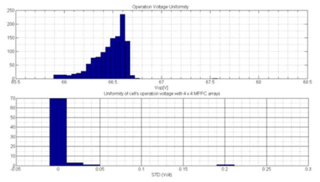
Operation voltage (Vop) distribution of 1200 cells and standard deviation of Vop with the assembled arrays after sorting.
Figure 6.

The alignment of crystal array with light guide and MPPC array.
2.3. Readout electronics
Figure7 shows the readout electronics chains for human and plant PET insert projects. The resistor network PCB board has the same size as the custom made MPPC array board; conventional discretized positioning circuits (DPC) are applied [19] for both projects. After the resistor network, 16 anode signals are reduced to 4 position encoded analog signals and fed into a 16-channel amplifier board which supports a total of 4 detector modules. The required signal charecteristics for Cardinal and QuickSilver electronics are different, so readout analog circuits are customized. For human insert applications, a simple voltage feedback fast amplifier board is used here and Figure8 shows the detailed circuit diagram and the actual PCB boards. For plant insert applications, the amplified signal is followed by a buffering stage, which also converts the signal from negative single-end to positive pseudo differential mode to be compatible with QuickSilver™ readout electronics. The silicon based photo multipliers are very sensitive to environmental temperature changes. To minimize the temperature fluctuation due to the heat generated by the amplifier boards, the detector modules are connected to the amplifier boards with 62-cm flat flexible cables. These long cables also allow us to place only the detector modules and their carbon fiber enclosure inside the scanners FOV to minimize Compton scatter that would otherwise be created by the amplifier boards. To maintain a constant gain of the MPPC detectors, a micro-controller (MIC) board that monitors temperature of detector modules by reading the signals from the temperature sensors mounted on individual detector modules was implemented for the human insert applications. This MIC controls a 32-channel high-voltage supply module (EVAL-AD5535EB, Analog Devices Inc.) and a stable MPPC gain is achieved by changing the bias voltage corresponding to the temperature change. For the plant insert applications, each of the 8 amplifier boards has an MIC; temperature monitoring and high voltage tuning is done by the amplifier board itself.
Figure 7.

Schematic diagram of readout electronics for human (top) and plant PET (bottom) insert system. Different amplifier circuits are used to provide different output analog signal characteristics that are compatible with Siemens’ clinical and pre-clinical PET scanners. For human PET insert application, a 32-channel high voltage supplier controlled by an MCU board functions MPPC bias voltage controlling and gain compensation. For plant PET insert application, this function is distributed to each amplifier board that has an MCU and 4-channel high voltage supplier integrated. DEA: Detector Electronics Assembly, MUX: Multiplexer board, GIM: Gantry Interface Module, ACS: Advanced Computer System, MCU:Microprogrammed Control Unit, EPM: Event Processing Module, ESR: Event readout Module.
Figure 8.

Upper: schematic diagrams of the DPC resistor network applied and the amplifier circuit. Lower: the picture of the 16-channel amplifier board used for flat panel detector readout.
The analog signals from the amplifier boards are sent to harness boards that provide the right signal assignment and cable connectors for the two different readout electronics systems. For human insert application, 6 extra detector electronics assemblies (DEAs) are added and the singles event from insert and scanner DEAs goes through a multiplexer board (MUX) before being sent to the coincidence processor. With this MUX, events from both detector systems are acquired simultaneously, without affecting the functionality of all the detectors in the original human PET scanner. For plant insert applications, the low resolution half-ring is disabled, and its corresponding electronics processing modules (EPM) are used to readout the insert detectors.
2.4. Testing system and settings
Figure9 shows the schematic diagram of the detector testing setup. A Ge-68 point source with 1.36 MBq (40 uCi) activity is used for all the tests performed here. The MPPC array in the detector works at 0.7 V over manufacturer recommended operation voltage. The detector module is kept at room temperature (about 22 °C) and singles data is acquired, which is used for the following crystal histogram calculation and energy resolution measurement. The total singles and coincidence events data acquisition is completed with a time duration of around 3 hours without temperature induced gain variation compensation.
Figure 9.

Schematic diagrams of the detector block testing system. The yellow blocks are standard NIM modules. Custom designed analog circuit boards are shown with green blocks. A commercial MicroTCA based multi-channel digitizing system is used for data acquisition.
The testing system used here is based on standard NIM modules (as defined in Figure9) and some custom designed analog circuit boards. A commercial MicroTCA based multi-channel digitizing system (uDigitizer, Nutaq Innovation Inc.) provides 32 ADC channels each running at 125 Msps with 14 bits precision. The analog signals from the fast amplifier board have 20 ns rising edge. A shaping circuit board is added to the signal path before the analog signals are sent to the uDigitizer. For timing measurement, a 3 × 3 × 20 mm3 LSO crystal is coupled to SensL’s FB series 3 mm SiPM cells with its fast output signal sent to the trigger circuit and acts as a reference detector. The timing performance of the reference detector is measured in [20] and the single photon timing resolution (SPTR) is around 200 ps with the working condition recommended, which is sufficient for evaluating our detector block’s timing performance.
For energy resolution, the acquired block flood histogram is first segmented to allocate the singles events to individual crystals. The crystal energy resolution is calculated by applying Gaussian fitting around the photon peak region of the energy spectra. All the energy resolution reported here does not include corrections for the non-linear response of the MPPC detectors.
Timing resolution for single crystals is calculated with +15/−15% energy window applied for individual crystals. The timing resolution of the whole block and its center 10 × 10 crystal array is calculated with +20/−20% energy window applied for valid events selection. Gaussian fitting is then used to calculate the timing performance parameters.
3. Results
3.1. Crystal separation capability
The flood histogram in Figure10 acquired with 1 M singles events shows excellent crystal separation capability, with all the 256 crystals clearly resolved. The profiles are also provided along row 8 and column 8 of the detector module. The measured average peak-to-valley ratios from row #8 and column #8 crystals are 3.2 and 3.5 respectively.
Figure 10.

Flood histogram and profiles (along of row #8 and column #8) of detector #612 (working at 0.7 V over manufacture recommended operation voltage).
3.2. Energy resolution
As shown in Figure11, the detector module has the mean, standard deviation, minimum (best) and maximum (worst) energy resolution of 10.19%, +/−0.68%, 8.36%, 13.45% FWHM, respectively. The detector exhibits good uniformity in terms of individual crystals’ energy resolution even for edge crystals. Two out the four corner crystals show the worst energy resolution, which was due to a slight misalignment of the light guide with the crystal array. The map of measured energy spectrum peak value of individual crystals is not consistent with the crystal energy resolution map, and demonstrates a special pattern. This is believed to be caused by the non-uniform gain for each charge injection point in the unsymmetrical DPC resistor network. Nevertheless, the energy resolution map shows that this did not have a significant impact on the uniformity of energy resolution for individual crystals. The energy resolution shown in Figure12 of the whole block is ~20% FWHM (~15% for the center 10 × 10 crystals, the region that light propagation is not affected by the cuts in the light guide).
Figure 11.

Left: crystal energy resolution map of the whole block. Right: photon peak (from raw data of ADC values) map of the whole block.
Figure 12.

Energy spectrum of the detector block (top), center 10 × 10 crystals (middle) and a single crystal (bottom).
3.3. Timing resolution
Figure13 shows the timing performance of a detector module with the mean, STD, minimum (best) and maximum (worst) time resolution of 0.95 ns, +/−0.08 ns, 0.79 ns, 1.55 ns FWHM, respectively. Figure14 shows the measured coincidence timing spectra with the whole block, center 10 × 10 crystals and single crystal (Column 6, Row 6) giving timing resolutions of 1.23 ns, 1.00 ns and 0.92 ns respectively. The measured results shows a uniform timing performance of most crystals. Although the five crystals at the center of one edge show the worst timing performance, their energy resolution is not the worst which mean the light loss is not the dominant factor. Figure13 also shows the map of time offset between individual crystals of the detector module and the reference detector. The measured variation is 0.37 ns and the maximum difference reaches1.60 ns. This timing degradation is most likely caused by the different transient time of individual MPPC cells and the length of connected traces on the PCB board; detailed calibration is required when using this MPPC array for Time-of-Flight applications. The block timing performance can be improved by applying a time lookup table for individual crystals. We expect the timing resolution between two detector modules to be better than 1.31 ns FWHM based on the measured mean time resolution, which performs better than the detectors in the Siemens Biograh scanner and is comparable with the detectors in the Siemens Inveon™ scanner.
Figure 13.
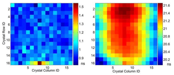
Left: crystal timing resolution map of the whole block. Right: time offset (with fast reference detector) map of the whole block detector.
Figure 14.

Timing spectrum of the detector block (top), center 10 × 10 crystals (middle) and a single crystal (bottom). 20%/−20% energy window is applied for valid events selection. The blue dotted curves represent the raw data and the red curve is the Gaussian fitting results.
3.4. Test with commercial scanners
Figure15 shows the layout of the flat panel detector under testing with commercial scanner electronics. Due to the similar readout electronics between Siemens’s pre-clinical and clinical scanners, the assembled detector blocks are only tested with Siemens Cardinal electronics. All the crystals are clearly separated in Figure16. The acquired flood histograms are similar to that acquired with the 14 bits 125 Msps ADCs in Figure10 and block energy spectra also look similar. The quality of the 4 consecutively assembled detector blocks are very consistent.
Figure 15.

The layout of a half-size prototype of flat panel detector device under testing including (a) support plate (made of black delrin now), (b) high voltage supply cables (high voltage supplier not shown), (c) long flat flexible cable for position encoded analog signals, (d) high resolution block detectors and (e) 16-channel amplifier boards.
Figure 16.
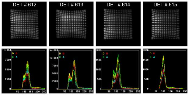
Flood histograms and energy spectra of assembled detector block #612–615 acquired with Siemens Cardinal electronics.
4. Conclusion
We have developed a versatile panel detector for multiple PET insert projects with VP-PET geometry. It features compact detector block design with custom built MPPC array, light guide and analog electronics. This design allows detector block to be tiled with 1 mm gaps. The new 4-side buttable (200 μm gaps) MPPC-based high resolution PET detectors demonstrate good performance in terms of crystal separation, energy (10.19+/−0.68%) and timing resolution (0.95 +/− 0.08 ns). These excellent characteristics are attributed to consistent performance of individual MPPC cells due to the new TSV process. Detectors tested with commercial scanner electronics show similar performance, demonstrating the compatibility of these compact detectors for the proposed VP-PET insert applications.
Acknowledgments
We would like to thank Stefan B. Siegel, Dongming Hu, John W. Young, Kenneth Puterbaugh of Siemens Molecular Imaging Inc. for technical support in using Siemens QuickSilver™ electronics for pre-clinical and Cardinal electronics for clinical PET scanners; and Lynne Jones from Washington University in St. Louis for proofreading the manuscript. This research was supported in part by the National Science Foundation (grant DBI-1040498) and in part by the National Institute of Health (grant R01CA136554).
Footnotes
Publisher's Disclaimer: This is a PDF file of an unedited manuscript that has been accepted for publication. As a service to our customers we are providing this early version of the manuscript. The manuscript will undergo copyediting, typesetting, and review of the resulting proof before it is published in its final citable form. Please note that during the production process errors may be discovered which could affect the content, and all legal disclaimers that apply to the journal pertain.
References
- 1.Tai Y-C, Wu H, Pal D, O’Sullivan Ja. Virtual-pinhole PET. J Nucl Med. 2008;49(3):471–9. doi: 10.2967/jnumed.107.043034. http://www.pubmedcentral.nih.gov/articlerender.fcgi?artid=3024474&tool=pmcentrez&rendertype=abstract. [DOI] [PMC free article] [PubMed] [Google Scholar]
- 2.Wu H, Pal D, O’Sullivan Ja, Tai Y-C. A feasibility study of a prototype PET insert device to convert a general-purpose animal PET scanner to higher resolution. J Nucl Med. 2008;49(1):79–87. doi: 10.2967/jnumed.107.044149. http://www.ncbi.nlm.nih.gov/pubmed/18077526. [DOI] [PubMed] [Google Scholar]
- 3.Wu H, Pal D, Song TY, O’Sullivan Ja, Tai Y-C. Micro insert: a prototype full-ring PET device for improving the image resolution of a small-animal PET scanner. J Nucl Med. 2008;49(10):1668–76. doi: 10.2967/jnumed.107.050070. http://www.pubmedcentral.nih.gov/articlerender.fcgi?artid=3021981&tool=pmcentrez&rendertype=abstract. [DOI] [PMC free article] [PubMed] [Google Scholar]
- 4.Qi J, Yang Y, Zhou J, Wu Y, Cherry SR. Experimental assessment of resolution improvement of a zoom-in PET. Phys Med Biol. 2011;56(17):N165–74. doi: 10.1088/0031-9155/56/17/N01. http://www.ncbi.nlm.nih.gov/pubmed/21828899. [DOI] [PubMed] [Google Scholar]
- 5.Mathews AJ, Komarov S, Wu H, O’Sullivan Ja, Tai Y-C. Improving PET imaging for breast cancer using virtual pinhole PET half-ring insert. Phys Med Biol. 2013;58(18):6407–27. doi: 10.1088/0031-9155/58/18/6407. http://www.pubmedcentral.nih.gov/articlerender.fcgi?artid=3890243&tool=pmcentrez&rendertype=abstract. [DOI] [PMC free article] [PubMed] [Google Scholar]
- 6.Brzeziski K, Oliver JF, Gillam J, Rafecas M. Study of a high-resolution PET system using a silicon detector probe. Phys Med Biol. 2014;59(20):6117–40. doi: 10.1088/0031-9155/59/20/6117. http://www.ncbi.nlm.nih.gov/pubmed/25254926. [DOI] [PubMed] [Google Scholar]
- 7.Wang Q, Mathews AJ, Li K, Wen J, Komarov S, O’Sullivan Ja, Tai Y-C. A dedicated high-resolution PET imager for plant sciences. Phys Med Biol. 2014;59(19):5613–29. doi: 10.1088/0031-9155/59/19/5613. http://www.ncbi.nlm.nih.gov/pubmed/25190198. [DOI] [PubMed] [Google Scholar]
- 8.Song TY, Wu H, Komarov S, Siegel SB, Tai Y-C. A sub-millimeter resolution PET detector module using a multi-pixel photon counter array. Phys Med Biol. 2010;55(9):2573–87. doi: 10.1088/0031-9155/55/9/010. http://www.pubmedcentral.nih.gov/articlerender.fcgi?artid=2975434&tool=pmcentrez&rendertype=abstract. [DOI] [PMC free article] [PubMed] [Google Scholar]
- 9.Yamamoto S, Yeom JY, Kamada K, Endo T, Levin CS. Development of an Ultrahigh Resolution Block Detector Based on 0.4 mm Pixel Ce : GAGG Scintillators and a Silicon Photomultiplier Array. 2013;60(6):4582–4587. [Google Scholar]
- 10.Seifert S, van der Lei G, van Dam HT, Schaart DR. First characterization of a digital SiPM based time-of-flight PET detector with 1 mm spatial resolution. Phys Med Biol. 2013;58(9):3061–74. doi: 10.1088/0031-9155/58/9/3061. http://www.ncbi.nlm.nih.gov/pubmed/23587636. [DOI] [PubMed] [Google Scholar]
- 11.Goertzen AL, McClarty MM, Berg EJ, Kozlowski P, Retiere F, Ryner L, Sossi V, Stortz G, Thompson CJ. Design and Performance of a Resistor Multiplexing Readout Circuit for a SiPM Detector. IEEE Trans Nucl Sci. 2013;60(3):1541–1549. doi: 10.1109/TNS.2013.2251661. http://ieeexplore.ieee.org/lpdocs/epic03/wrapper.htm?arnumber=6495512. [DOI] [Google Scholar]
- 12.Schaart DR, Seifert S, Vinke R, van Dam HT, Dendooven P, Löhner H, Beekman FJ. LaBr(3):Ce and SiPMs for time-of-flight PET: achieving 100 ps coincidence resolving time. Phys Med Biol. 2010;55(7):N179–89. doi: 10.1088/0031-9155/55/7/N02. http://www.ncbi.nlm.nih.gov/pubmed/20299734. [DOI] [PubMed] [Google Scholar]
- 13.Pichler BJ, Swann BK, Rochelle J, Nutt RE, Cherry SR, Siegel SB. Lutetium oxyorthosilicate block detector readout by avalanche photodiode arrays for high resolution animal PET. Phys Med Biol. 2004;49(18):4305–4319. doi: 10.1088/0031-9155/49/18/008. http://stacks.iop.org/0031-9155/49/i=18/a=008?key=crossref.00c0a072c73b78ccb7b136a459be0869. [DOI] [PubMed] [Google Scholar]
- 14.Shao Y, Sun X, Lan Ka, Bircher C, Lou K, Deng Z. Development of a prototype PET scanner with depth-of-interaction measurement using solid-state photomultiplier arrays and parallel readout electronics. Phys Med Biol. 2014;59(5):1223–38. doi: 10.1088/0031-9155/59/5/1223. http://www.ncbi.nlm.nih.gov/pubmed/24556629. [DOI] [PMC free article] [PubMed] [Google Scholar]
- 15.Yamamoto K, Sato K, Yamada R, Hosokawa N, Nagano T, Hayatsu K, Shimohara T, Ohkuwa Y, Oguri A. Assembly technology of 4-side buttable MPPC. Nucl Instruments Methods Phys Res Sect A Accel Spectrometers, Detect Assoc Equip. 2013;732:547–550. doi: 10.1016/j.nima.2013.07.004. http://linkinghub.elsevier.com/retrieve/pii/S0168900213009807. [DOI] [Google Scholar]
- 16.Shimizu K, Uchida H, Sakai K, Hirayanagi M, Nakamura S, Omura T. Development of a Multi-Pixel Photon Counter Module for Positron Emission Tomography. IEEE Trans Nucl Sci. 2013;60(3):1512–1517. doi: 10.1109/TNS.2013.2251657. http://ieeexplore.ieee.org/lpdocs/epic03/wrapper.htm?arnumber=6495516. [DOI] [Google Scholar]
- 17.Nagano T, Hosokawa N, Ishida A, Tsuchiya R, Sato K, Yamamoto K, Samples AM. 2013 IEEE Nucl Sci Symp Med Imaging Conf (2013 NSS/MIC) IEEE; 2013. Timing resolution dependence on MPPC geometry and performance; pp. 1–5. http://ieeexplore.ieee.org/lpdocs/epic03/wrapper.htm?arnumber=6829681. [DOI] [Google Scholar]
- 18.Newport DF, Siegel SB, Swann BK, Atkins BE, McFarland AR, Pressley DR, Lenox MW, Nutt RE. 2006 IEEE Nucl Sci Symp Conf Rec. IEEE; 2006. QuickSilver: A Flexible, Extensible, and High-Speed Architecture for Multi-Modality Imaging; pp. 2333–2334. http://ieeexplore.ieee.org/xpls/abs_all.jsp?arnumber=4179495 http://ieeexplore.ieee.org/lpdocs/epic03/wrapper.htm?arnumber=4179495. [DOI] [Google Scholar]
- 19.Siegel S, Silverman R, Cherry S. Simple charge division readouts for imaging scintillator arrays using a multi-channel PMT. IEEE Trans Nucl Sci. 1996;43(3):1634–1641. doi: 10.1109/23.507162. http://ieeexplore.ieee.org/lpdocs/epic03/wrapper.htm?arnumber=507162. [DOI] [Google Scholar]
- 20.Yeom JY, Vinke R, Pavlov N, Bellis S, Wall L, O’Neill K, Jackson C, Levin CS. Fast Timing Silicon Photomultipliers for Scintillation Detectors. IEEE Photonics Technol Lett. 2013;25(14):1309–1312. doi: 10.1109/LPT.2013.2264049. http://ieeexplore.ieee.org/lpdocs/epic03/wrapper.htm?arnumber=6530701. [DOI] [Google Scholar]