Abstract
We have batch-fabricated cantilevers with ~100 nm diameter nickel nanorod tips and force sensitivities of a few attonewtons at 4.2 kelvin. The magnetic nanorods were engineered to overhang the leading edge of the cantilever and, consequently, the cantilevers experience what we believe is the lowest surface noise ever achieved in a scanned probe experiment. Cantilever magnetometry indicated that the tips were well magnetized, with a ≤ 20 nm dead layer; the composition of the dead layer was studied by electron microscopy and electron energy loss spectroscopy. In what we believe is the first demonstration of scanned probe detection of electron-spin resonance from a batch fabricated tip, the cantilevers were used to observe electron-spin resonance from nitroxide spin labels in a film via force-gradient-induced shifts in cantilever resonance frequency. The magnetic field dependence of the magnetic resonance signal suggests a non-uniform tip magnetization at an applied field near 0.6 T.
Development of technologies ranging from biosensors and theraputics to flexible circuits and energy conversion devices would be greatly accelerated if better metrology tools were available for probing the structure and chemical composition of individual organic nanostructures. Unfortunately, our ability to characterize organic material at nanometer spatial resolution — in three dimensions, nondestructively, and with chemical specificity — lags far behind our ability to synthesize new materials and direct their nanoscale organization. For this reason, the recent demonstration of 4-nm resolution proton magnetic resonance imaging of a single virus1 is a particularly exciting advance.
In the experiment of Reference 1, the sample was deposited onto the 0.3 µm × 1.0 µm leading edge of a fragile high-compliance silicon microcantilever and transferred to high vacuum and millikelvin temperatures; magnetic resonance signal from the sample was detected by irradiating the sample with radiowaves while observing the force between the sample’s protons and a nearby 200 nm diameter FeCo cone. Having to prepare the sample on the end of an extremely small and very fragile cantilever would appear to preclude the study of a wide range of samples, such as functioning organic electronic devices and cryopreserved biomolecules. “Scanned probe” detection of both electron-spin2,3 and nuclear magnetic resonance4–6 has been demonstrated, but so far only with cantilevers having micron-scale lithographically defined magnets5 or whose magnetic tips were affixed manually2–4,6 and whose diameters were limited to ~150 nm by ion damage from focussed-ion beam milling (FIB).3,6,7
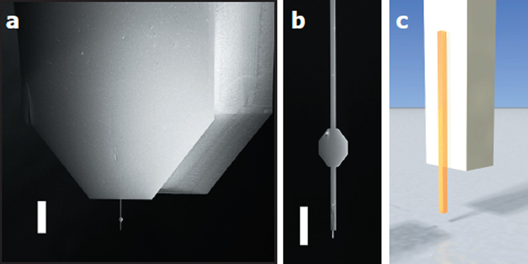
Here we report an approach to batch-fabricating attonewton-sensitivity silicon microcantilevers with integrated nickel tips only 70 nm wide. To obviate the problem of ion-beam damage, the magnetic tips are produced by electron beam lithography, evaporation, and liftoff, which can produce sub-50 nm wide tips with further optimization. The top-down approach to MRFM cantilever fabrication presented here involves thirty-eight carefully-integrated processing steps, including three electron beam lithography steps and two optical lithography steps, each requiring registration to all previous steps. To achieve large magnetic field gradients while simultaneously minimizing surface noise, the integrated magnetic tips consist of a narrow magnetic nanorod that overhangs the cantilever’s leading edge (Figure 1). The key feature of our design is that it keeps the large-cross-section silicon body of the cantilever many hundreds of nanometers away from the sample surface while simultaneously enabling the magnetic nanorod to approach within a few nanometers of the sample’s spins.
Figure 1.
Force microscope cantilever for nanoscale magnetic resonance imaging. (a) Ultrasensitive cantilever (scale bar = 200 µm); (b) magnified view of the cantilever showing a reflective pad for interferometric detection of cantilever motion (upper) and a narrowed leading edge (lower) to minimize cantilever-sample interactions (scale bar = 30 µm); and (c) sketch of a ~100 nm wide magnetic nanorod tip overhanging the cantilever’s leading edge.
Our main finding is that these overhanging tips maintain attonewton force sensitivity to much smaller tip-sample separations than demonstrated before. This finding establishes that careful engineering of the cantilever’s leading edge is a viable approach to significantly improve the sensitivity of mechanically detected magnetic resonance.
We demonstrate the magnetic integrity of the tips via cantilever magnetometry measurements of tip saturation magnetization and coercivity.8–10 Moreover, we use the tips to detect electron-spin resonance from an organic free radical in a film11 — the first time that a batch-fabricated tip has been used to detect electron-spin resonance in a magnetic resonance force microscope experiment. Taken together, these results significantly advance the feasibility of scanned-probe nanoscale magnetic resonance imaging of as-fabricated thin-film samples and devices.
Results
Cantilever nanofabrication
Nanofabrication strategy
Micron-scale magnets have previously been defined by optical lithography and batch fabricated on high-compliance torsional5,12 and cantilevered-beam13 mechanical resonators for use in MRFM experiments. Patterning of submicron-scale magnets on high-compliance mechanical resonators has been achieved by electron-beam lithography14 and focussed-ion beam milling.12 The approaches of references 12 and 14, however, are not suitable for placing magnets near the leading edge of the cantilever, as required for scanned-probe work, and do not address or mitigate damage introduced by focussed-ion beam milling.3,6,7
While a number of non-FIB approaches for fabricating magnetic tips as small as tens of nanometers on commercial atomic-force microscope cantilevers have been developed for magnetic force microscopy (MFM), these approaches are ill-suited for fabricating MRFM tips on high-compliance cantilevers, for a number of reasons.
The primary source of noise in the highest-sensitivity MRFM experiments to date has been surface-related force noise or frequency noise.1,15,16 The cause of this noise, at least for metal coated samples at low temperature, is unknown, but is thought to arise from charges near the cantilever’s leading edge interacting with electric-field17,18 and field-gradient fluctuations19 in the sample. To achieve high sensitivity in an MRFM experiment, it is therefore crucially important to mitigate this interaction by minimizing the cross sectional area of the cantilever nearest the surface. This requirement makes MFM-tip fabrication protocols involving evaporation onto the cantilever sidewall,9 evaporation of metal followed by focussed ion-beam milling,20–23 and evaporation through a nanopore24 poorly suited for making high-sensitivity MRFM tips.
In contrast with MFM, where the smallest-diameter tip is best for imaging, the imaging of subsurface spins in an MRFM experiment requires a tip diameter comparable to the sample depth.16,25 The ideal MRFM tip-fabrication protocol must therefore produce tips having a range of diameters, from approximately 500 nm to below 50 nm. Numerous approaches exist for making a magnetic tip like the one sketched in Figure 1(c) with a diameter in this range: electron beam deposition of metals from organic precursors;26 electron beam deposition of carbon followed by blanket evaporation of metal;27–29 evaporation onto a carbon nanocone30 or carbon nanotube;31,32 using the magnetic catalyst particle at the end of a multiwalled carbon nanotube;33,34 preparation of metal-filled carbon nanotubes;35 and dielectrophoretic assembly of magnetic nanorods.36 Unfortunately these approaches are serial, require significant human control, and yield tips with large device-to-device variation. Although arrays of singly-clamped metallic nanowires have recently been batch-fabricated in high yield using electric-field and capillary-force assisted self assembly,37,38 it is hard to see how to integrate the required sacrificial electrodes into a protocol for fabricating attonewton-sensitivity cantilevers.14,39 In contrast, the approach demonstrated here for creating attonewton-sensitivity cantilevers with integrated overhanging nickel nanorod tips is amenable to wafer-scale production of cantilevers.
Cantilever material
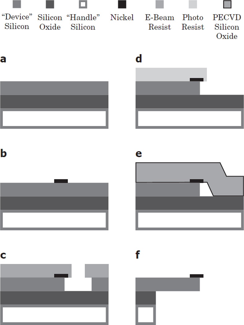
We began with a silicon-on-insulator (SOI) wafer14,39 whose 〈100〉-oriented single-crystal silicon device layer had a thickness of 340 nm, a buried silicon oxide layer thickness of 400 nm, and a handle wafer thickness of ~500 µm (Figure 2(a)).
Figure 2.
Schematic drawing of the fabrication process. The process starts with a silicon-on-insulator wafer, (a), onto which a nickel magnet is deposited, (b). Isotropic etching is used to partially remove the silicon under the magnet, (c). A second etch defines the body of the cantilever, (d). After the cantilever is defined, a protective silicon oxide layer is deposited, (e). The handle silicon under the cantilever is removed using an anisotropic plasma etch, stopping on the buried silicon oxide layer; a two-layer photoresist and silicon oxide mask is used (not shown). The silicon oxide layers are then removed by a hydrofluoric acid etch, followed by CO2 critical point drying, to yield the cantilever sketched in (f).
Alignment Marks
The first step in the fabrication process was preparation of alignment marks. Designing the alignment marks and choosing the alignment-mark material carefully was crucial because of the mixed modes of lithography used in the fabrication process, involving different tools with different aligning strategies.40 All device-layer features were aligned to marks defined in a single write by e-beam lithography. Defining the alignment marks and magnetic nanorods in the same lithographic step using the same material worked well, but only for nickel or cobalt nanorods thicker than about 200 nm, which is greater than our target size of 50 nm. The usual e-beam alignment-mark strategy of etching ≥ 1 µm deep trenches into the substrate proved problematical with SOI wafers. A single-step CF4 reactive ion plasma etch yielded trenches with sufficiently vertical sidewalls, but an unreasonably thick e-beam resist (> 2 µm) was required because of the low selectivity of the CF4 etchant to poly(methyl methacrylate) e-beam resist. An alternative three-step reactive ion etch using SF6/O2 and CHF3 to remove silicon and silicon oxide, respectively, produced sufficiently deep trenches but left the trench sidewalls too sloped and uneven for them to serve as high-resolution e-beam alignment marks. Defining metal alignment marks and magnets in separate e-beam process solved these problems. Platinum and tungsten were evaluated because they have high atomic number, chemical stability, and – unlike gold – their presence in chemical vapor deposition chambers is tolerated. Platinum marks could be prepared via electron-beam evaporation and liftoff, while tungsten had to be sputtered over the whole wafer and then etched to define alignment marks. Marks made from both materials performed well; platinum marks were chosen for simplicity. Typical alignment accuracy was better than ±30 nm for electron-beam lithography features, and better than ±500 nm for optical lithography features.
Magnet material
Due to their ease of deposition, elemental magnetic materials were chosen over more complicated alloys such as PrFeB3,41 or SmCo.15 There were several reasons for the selection of nickel over materials such as iron or cobalt, both of which have a higher saturation magnetization. For iron, the primary concern was oxidation of the magnetic material during or after the fabrication process. In Ref. 14, Jenkins et al. suggested that oxidation of submicron nickel nanorods during the processing of cantilevers similar to ours is not a concern. Cobalt has a propensity to form silicides and has low resistance to etching by hydrofluoric acid. In control experiments, Co showed significant damage after 2 minutes of exposure to 6:1 buffered hydrofluoric acid, whereas Ni could withstand 6–8 minutes of exposure. Further experiments indicated that Co is more susceptible to silicide formation, at least in our fabrication process. We note that this is not indicated in the literature, which generally gives similar formation temperatures for Co42 and Ni43 silicides.
Nickel was also chosen because at high magnetic field it is expected to exhibit smaller tip magnetization fluctuations than either cobalt or iron.10 For MRFM experiments at low magnetic field, one wants a tip material with high coercivity to suppress magnetization fluctuations.3,41 At high magnetic field, however, Ng, Jenkins, and Marohn have shown experimentally that a nickel tip exhibits much smaller low-frequency transverse magnetization fluctuations than cobalt.10 The rationale for this observation is that at high field, applying the external field suppresses angular fluctuations of the tip magnetization more effectively in the lower anisotropy material.
Magnet definition
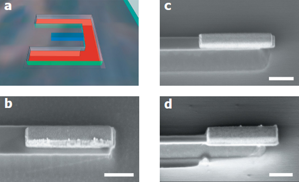
Nickel magnets were defined and deposited in the same manner as the alignment marks (Figure 2(b)). Nickel magnets of thicknesses 50, 100, and 200 nm and widths between 70 and 600 nm were prepared; all magnets were 1500 nm long. Magnet overhang was achieved via e-beam lithography followed by isotropic plasma etching (Figure 2(c)). As illustrated in Figure 3(a), a U-shaped “etch pit” was defined, positioned such that the base of the “U” was 50 nm from the end of the magnet. A carefully timed and calibrated isotropic SF6/O2 plasma etch was used to remove silicon vertically, down to the buried silicon oxide layer, as well as laterally, undercutting the resist by 200 to 400 nm (Figure 3(b–d)). This step also defined the width and length of the narrowed cantilever tip. The body of the cantilever was defined via optical lithography and a second SF6/O2 plasma etch (Figure 2(d)). The cantilevers were ~200 µm long and ~4 µm wide.
Figure 3.
Magnet underetch process. (a) Rendering of the etching process, halfway to completion, with the magnet (in blue) lying under the patterned resist. The device silicon (orange) has been etched under the resist layer, but is not yet removed down to the buried silicon oxide. (b–d) SEM images showing the etch process after (b) 10 s, (c) 20 s and (d) 30 s of etching. The resist has been removed for clarity. Scale bars are 500 nm.
Backside processing
Silicon oxide layers were deposited on both sides of the wafer by plasma-enhanced chemical vapor deposition (Figure 2(e)). The purpose of the front silicon oxide was to protect the magnets and cantilevers during backside wafer processing. The back silicon oxide served as a mask for a subsequent thru-wafer silicon etch to remove the handle-wafer silicon beneath the cantilever. A sacrificial photoresist mask layer was defined on top of the back silicon oxide using contact lithography and the mask pattern transferred from the photoresist to the underlying silicon oxide via a plasma etch. The purpose for this two-layer mask was to eliminate potential photoresist contamination during the penultimate processing step, the cantilever release etch.
Backside silicon etching, to remove the supporting handle-wafer silicon under the cantilevers, was performed using a Bosch-process anisotropic silicon etch. This etch, unexpectedly, introduced one of the major difficulties in the fabrication process — the formation of nickel silicide. Nickel forms a silicide at an appreciable rate at approximately 200°C and above.43 SEM observation of the nickel magnets at various times following the start of the backside etch showed that amorphous features began to grow from the nickel magnets when ~100 µm of the handle wafer remained to be etched. We speculate that as the backside silicon is etched away, the heat generated during the etch was less and less efficiently removed, increasing the magnet temperature. We overcame this problem by limiting the duration of uninterrupted etching time, and letting the tool cool between etches.
Release
The cantilevers were released in a buffered hydrofluoric acid solution. Following several rinses in deionized water and isopropanol, the cantilevers were removed from solution via critical point drying in CO2 (Figure 2(f)). The tip of a completed cantilever can be seen in Figure 4(a).
Figure 4.
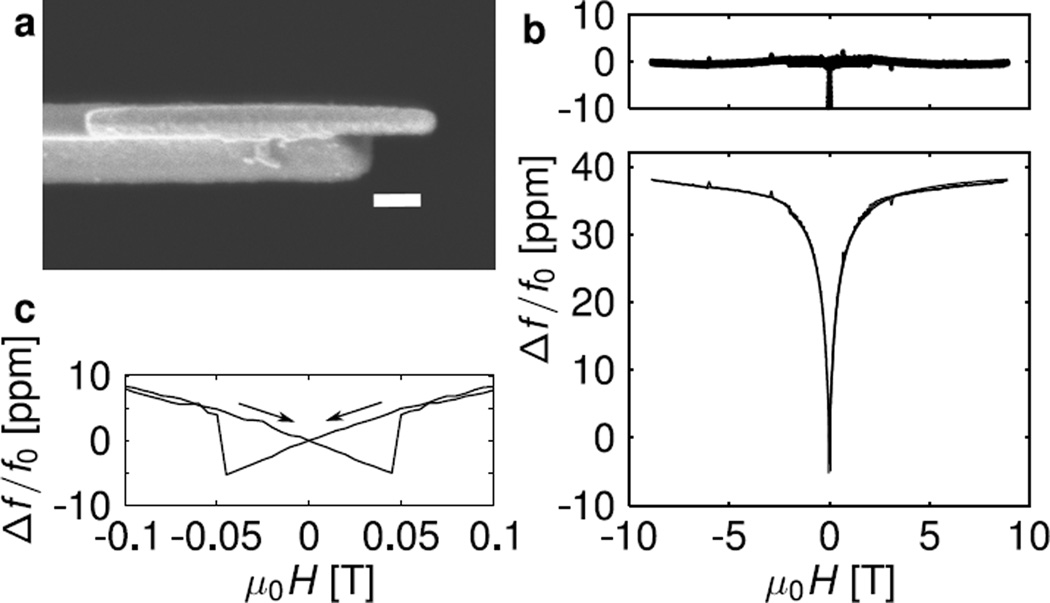
(a) Scanning electron micrograph of the cantilever’s leading edge, showing a nickel nanorod tip overhanging the cantilever’s leading edge by 350 nm (scale bar = 200 nm). (b) Characterization of the cantilever tip’s nickel nanorod by frequency-shift cantilever magnetometry. Fractional cantilever frequency shift versus field in parts per million (middle; solid line), the best-fit curve (middle; dotted line, indistinguishable from the data), and fit residuals (top). (c) Expanded view of the observed frequency shift near zero field, showing hysteresis.
Cantilever characterization
Cantilever magnetometry
Frequency-shift cantilever magnetometry was used to quantify the net magnetization and coercivity of the nanorod tip. Measurements were carried out in high vacuum (P = 10−6 mbar) at low temperature (T = 4.2 K). A magnetic field was applied along the long axis of the cantilever and the field swept while cantilever frequency was monitored. From a plot of cantilever frequency versus magnetic field (Figure 4(b)) we infer a tip magnetic moment of μobs = 5.25 ± 0.79 × 10⁻¹⁵ Am2, within 57 to 77% of the magnetic moment expected from the magnetization of bulk nickel (μ0Msat = 0.60 T) and measured volume (V = 1.64 × 10⁻²⁰m3). At low field, the frequency versus field data shows hysteresis consistent with switching at a coercive field of μ0Hc = 50 mT (Figure 4(c)). These results are encouraging and indicate that the many processing steps required to fabricate the cantilevers and create overhanging tips do not significantly affect the tip magnetic properties.
Surface noise
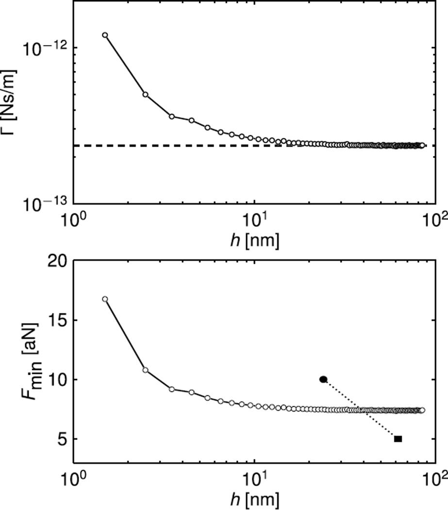
In Figure 5 we plot the friction coefficient Γ experienced by a representative cantilever near a gold-coated surface as a function of tip-sample separation. For comparison, the dotted line is the dissipation due to internal friction in the cantilever alone. We can see that the surface-induced cantilever dissipation is negligible at tip-sample separations above h = 10 nm.
Figure 5.
Top: Cantilever friction coefficient Γ versus tip-sample separation h. Bottom: The minimum detectable force versus tip-sample separation for our tip (empty circles) and for the tip reported in Ref. 1 (filled circle and square).
To compare our observed friction to what has been measured in the most sensitive MRFM experiment to date, we convert the measured friction coefficient to an equivalent minimum detected force using Fmin = (4kbT Γb)1/2 where kb is Boltzmann’s constant, T is temperature, and b is detection bandwidth. In Figure 5 we plot Fmin versus tip-sample separation assuming a temperature of T = 4.2 K and a detection bandwidth of b = 1 Hz (full circles). For comparison, we plot Fmin reported at two tip-sample separations in the recent 4 nm NMR imaging experiment of Ref. 1 carried out at T = 0.3 K (filled circle and square). Our cantilever’s force sensitivity is worse at large tip-sample separations, as expected since we are operating at a much higher temperature. In the experiment of Ref. 1, the minimum detectable force degraded to 10 aN at a tip-sample separation of h = 24 nm. Our magnetic-tipped cantilever, in contrast, maintains Fmin ≤ 10 aN for tip-sample separations down to h = 3 nm. The ability to maintain excellent force sensitivity while operating at close separation, to maximize the magnetic field gradient acting on the spin, is critical to achieving high spin sensitivity in an MRFM experiment.16
Cantilever frequency noise6,19 was also examined as a function of tip-sample separation. As expected,19 surface-induced frequency noise dominated internal-friction frequency noise at much larger tip-sample separations (h ≤ 60 nm). Frequency noise power spectra as a function of tip-sample separation can be found in Supporting Information.
Electron microscopy and spectroscopy
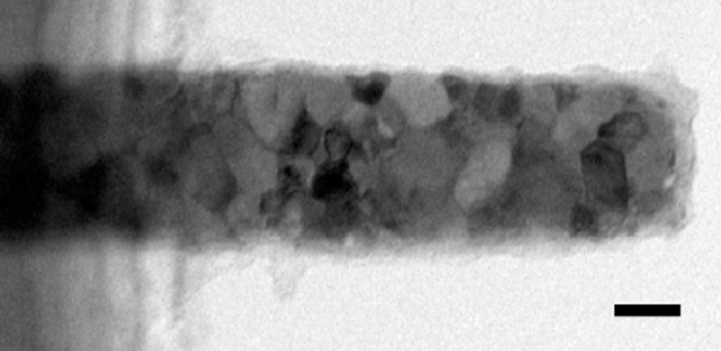
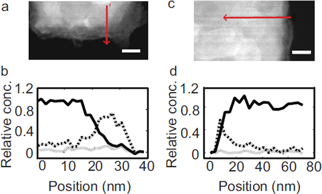
Scanning transmission electron microscopy (STEM) and electron energy loss spectroscopy (EELS) experiments were conducted to corroborate the presence of a damage layer on the nanorods. A second cantilever with an overhanging nanorod tip was prepared separately, from a second starting wafer, and sacrificed for STEM and EELS analysis. A top-down bright-field STEM image of the overhanging region of a representative nickel nanorod can be seen in Figure 6. Strong grain boundary contrast indicates that the bulk of the nanorod is polycrystalline, with a grain size of 20 to 40 nm, while the leading and side edges appear amorphous. EELS spectra were acquired to assay the elemental composition of the magnets with nanometer resolution. Spectra were acquired in linescans directed along the leading edge (Figure 7(a,b)) and side edge (Figure 7(c,d)). In both spectra, the only observed elements were chromium, nickel, and oxygen. Nearest the center of the nanorod the Cr:Ni ratio was 0.05:1, in excellent agreement with the 5:100 ratio expected given the thicknesses recorded during deposition. At both the leading edge and the side edge the nickel concentration decreases and the oxygen concentration increases. In Figure 7(b), the concentration of nickel begins to decrease 20 nm before the leading edge of the nanorod, implying a damage layer of 20 nm. In Figure 7(d), a 14 nm thick damage layer is observed. It should be noted that although the O:Ni ratio of 1:1 in the damage region at the nanorod side edge could correspond to the formation of NiO, the anomalously high O:Ni ratio at the leading edge cannot be explained solely by the formation of an oxide layer. Further studies will be required to understand the presence of this additional oxygen at the leading edge.
Figure 6.
Bright-field scanning transmission electron microscopy (STEM) image of a nickel nanorod overhanging the cantilever’s leading edge (scale bar = 50 nm).
Figure 7.
Elemental mapping of an overhanging nickel nanorod by electron energy loss spectroscopy (EELS). Lines indicate the scanning direction. Leading edge (a) STEM image and (b) EELS signal. Side edge (c) STEM image and (d) EELS signal. The scale bars in (a) and (c) represent 20 nm. In the EELS scans of (b) and (d), nickel, oxygen, and chromium are plotted using solid, dot-dash, and dotted lines, respectively.
Force-gradient detection of electron-spin resonance
To show that the tip’s leading edge was well magnetized, the cantilever in Figure 4(a) was used to detect electron-spin resonance mechanically from a nitroxide free radical using a force-gradient approach4,6 modified to observe fast-relaxing spins.11 The sample was a 230 nm thick film of 40 mM TEMPAMINE in perdeuterated polystyrene having a spin-lattice relaxation time of T1 = 1 ms and a spin-echo dephasing time of T2 = 450 ns (as measured by pulsed inductively-detected electron-spin resonance). The sample was coated with 20 nm of gold. Operating at 4.2 K and 10−6 mbar, the cantilever was brought to 60 nm above the sample surface in the geometry of Figure 1(c) and driven to a peak-to-peak amplitude of 80 nm. A static magnetic field was applied along the width of the cantilever4,8 which mitigates damping of the cantilever arising from tip-field interactions.2 To saturate sample spins, a cantilever-synchronized train of 17.6 GHz microwave pulses was applied to the sample, modulated at 9.56 Hz. Each pulse lasted for 6 cantilever cycles, followed by 6 cycles without microwave irradiation. To extract the resulting spin-induced modulation of the cantilever frequency, a digitized trace of cantilever displacement was sent to a software frequency demodulator followed by a lock-in amplifier.
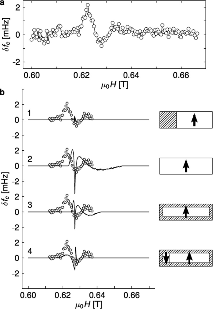
The measured spin-induced cantilever frequency shift is shown in Figure 8(a) as a function of applied magnetic field. We attribute the negative-going high-field peak in Figure 8(a) to a small number of spins just below the tip, where the field from the tip opposes the applied static magnetic field. The amplitude and lineshape of the mechanically detected resonance signal – particularly the “local” high-field peak – is a very sensitive function of the shape and magnetization of the tip’s leading edge.1,15,44,45
Figure 8.
Force-gradient electron-spin resonance signal acquired using the cantilever in Figure 4. (a) Observed cantilever frequency shift (circles) compared to numerically-calculated signal for various models of tip magnetization (solid lines; Models 1 to 4 going from to top bottom). Here white regions represent fully magnetized nickel and cross-hatched regions represent damaged nickel.
In Figure 8(b) we compare the observed signal to signal calculated numerically by modeling the tip as a uniformly magnetized cuboid. The sample temperature was taken to be T = 11 K based on prior work with larger tips affixed to the cantilever by hand. Assuming that the entire overhanging region was damaged and nonmagnetic gives a calculated signal that was far smaller than the observed signal (Model 1). Assuming a fully magnetized tip (Model 2), on the other hand, overestimates the signal size and the width of the local signal, corroborating the existence of a damage layer. For reference, we note that the large negative-going central peak in these simulations arises from a “bulk” resonance4,11 of far-away spins which experience little tip field. In Model 3 we assume a uniform 12 nm thick magnetic dead layer. This model better reproduces the width of the local signal, but misses the signal present downfield from the bulk signal. The downfield signal must be due to sample spins experiencing a tip field which is parallel to the applied static magnetic field. To account for the presence of downfield signal, in Model 4 we introduce a 50 nm wide domain at the leading edge of the tip magnetized anti-parallel to the applied field; the agreement between simulated and observed lineshape is still poor. While comparing the width and magnitude of the observed and simulated signal seen in Figure 8(b) allows us to conclude that the tip’s leading edge is magnetized with a damage layer no thicker than approximately 20 nm, in rough agreement with electron microscopy, none of the tip-damage scenarios fit the data very well.
The comparatively poor agreement between simulation and experiment apparent in Figure 8(b) is surprising, given the quantitative agreement demonstrated in Ref. 11 in an identical experiment carried out with a ~10 µm diameter spherical nickel tip. Our simulations approximate the tip as an ideal cuboid having uniform magnetization and assume that the cantilever amplitude is zero; additional simulations with a more realistic tip shape and accounting for the finite cantilever amplitude did not substantially improve the agreement between simulation and experiment. This suggests to us that the tip is not uniformly magnetized. This hypothesis is reasonable given the moderate operating field and the presence of (antiferromagnetic) nickel oxide at the tip surface. Another hypothesis is that the tip magnetization is changing during the magnetic field sweep. Further experiments with less damaged tips at higher field will be required to resolve the source of the puzzling simulation-experiment disagreement seen here.
Discussion
Our main finding is that the force noise (or equivalently, dissipation) experienced by our cantilevers is, we believe, the smallest ever demonstrated for an object located only a few nanometers from a surface. This finding establishes that careful engineering of the cantilever’s leading edge is a viable approach to significantly improving the sensitivity of mechanically detected magnetic resonance.
The main challenge to fabricating magnetic nanorod tips overhanging the leading edge of attonewton-sensitivity cantilevers was the mitigation of heat-induced metal silicide formation. This we achieved, but at low yield. Once deposited, low-temperature processing of the tip material is clearly essential to achieving high yield. Both magnetometry and MRFM data indicated the presence of a magnetically dead layer at the cantilever’s leading edge. The STEM and EELS data showed that the main component of the magnetic dead layer was NiO, with extra oxygen contamination present on the leading edge. No silicon was detected by EELS, corroborating that our careful thermal management during the Bosch etch succeeded in mitigating nickel silicide formation, at least for the magnets which survived HF release. Additional control experiments indicated that nickel was most likely being oxidized during the PECVD deposition of oxide and not during the aqueous HF release. These findings suggest that future development should focus on protecting the magnet during oxide deposition.
The 100 nm wide tips were successfully used to observe electron-spin resonance, the first time to our knowledge that electron-spin resonance has been detected using a batch-fabricated magnetic-tipped cantilever. In these force-gradient electron-spin resonance experiments the dominant source of noise was unfortunately surface-related fluctuations in cantilever frequency and not force noise. We see no reason, however, that the cantilevers presented here could not be used in a force-detected magnetic resonance experiment immediately. Force experiments are challenging for electron spins because of the high microwave magnetic fields required but for nuclear spins an oscillating magnetic field large enough for force detection can be achieved at cryogenic temperatures with microwires1,46 (not available in our apparatus). Moore et al. recently introduced a method for up-converting a slowly-modulated force-gradient spin signal into a cantilever-resonant force signal, thereby evading surface frequency noise.47 This method could allow force-noise-limited detection of electron-spin resonance with the cantilevers presented here.
The magnetic field gradients produced by our tips are competitive with the largest gradients used in an MRFM experiment to date. With the magnetic field applied along the width of the tip and assuming a uniform dead layer of 20 nm, we estimate the relevant magnetic field gradient at a distance 5 nm from the nickel magnet surface to be 8.27 × 10⁵ T/m. For a field applied along the tip’s long axis, the relevant gradient strength improves to 2.78 × 10⁶ T/m, which would give a single-electron force of 28 aN. By replacing nickel with cobalt or by slightly reducing the dead layer thickness, it seems feasible to achieve a gradient comparable to the 4.2 × 10⁶ T/m of Reference 1, which would enable 4 nm imaging of nuclear spins in as-fabricated samples. The poor agreement between calculated and observed signal lineshapes is a cause for concern, however, since a uniformly magnetized tip is probably necessary for image reconstruction.1 Further experiments will be required to establish whether achieving a uniformly magnetized tip will require elimination of (antiferromagnetic) oxide, operation at higher applied field, or both.
We believe tips with diameters even smaller than 70 nm can be manufactured by improving the electron-beam lithography step defining the magnet; whether the dead layer can be reduced by thermal management or encapsulation remains an open question. Such improved cantilevers would be useful for measuring small mechanical forces between metals and dielectrics under irradiation,48 observing tip-enhanced Raman spectroscopy,49 and imaging the electric field and field-gradient fluctuations arising from charge motion and thermal dielectric fluctuations.19
The cantilevers presented here already open up exciting possibilities for carrying out sub-10 nm resolution magnetic resonance imaging studies of as-fabricated electronic devices and prepared biological samples where mounting the sample to the cantilever is impossible or impractical. The ability to implement “scanned probe” MRFM is particularly crucial for biological samples, where sample preparation protocols developed for cryo-electron microscopy such as flash freezing in glass-forming matrices50 will probably be required to preserve the structural integrity of biomacromolecules and biomacromolecular complexes at cryogenic temperatures.
Methods
Cantilever fabrication
Metals were obtained from Kurt J. Lesker; silicon-on-insulator (SOI) wafers were obtained from SOITEC; solvents were obtained from Fisher Scientific or J. T. Baker and used as received. The SOI wafer’s device layer resistivity was 14 – 22Ωcm, corresponding to a boron dopant density of 6 – 9 × 1014 cm−3. Alignment marks for both electron-beam and optical lithography steps were defined in a resist bilayer consisting of ~50 nm of 950,000 molecular weight (MW) (poly)methylmethacrylate (PMMA) on top of ~550 nm of 495,000 MW PMMA (Microchem, supplied in either anisole (495,000 MW resist) or methyl isobutyl ketone (950,000 MW resist)). All electron-beam lithography was done on a JEOL JBX9300FS tool (100 KeV beam, 2 nA current). The resist was developed in a 1:3 methyl isobutyl ketone: isopropanol solution. A 5 nm thick chrome (99.95% purity) adhesion layer followed by a 100 nm thick layer of platinum (99.9% purity) were deposited on the wafer by electron beam evaporation (CVC products SC 4500 evaporator). Finally, the resist and excess metal were removed by dissolution in a 1:1 methylene chloride : acetone solution, aided by approximately one minute of sonication.
To prepare the magnets, the thickness of the 495,000 MW PMMA layer was varied according to the dimensions of the magnet being fabricated, with the resist being approximately 4× thicker than the desired magnet thickness. A 5 nm Cr adhesion layer (99.95% purity; 0.20 to 0.25 nm/s) and a 50 to 100 nm Ni layer (99.995% purity; 0.25 nm/s) were deposited by electron-beam evaporation. The magnet “etch pit" was written by e-beam lithography in ~700 nm thick 495,000 MW PMMA. The wafer was etched for 30–40 seconds in an SF6/O2 plasma (Oxford Instruments Plasmalab 80). The resist was then removed by dissolution in a 1:1 methylene chloride:acetone solution, aided by approximately one minute of sonication. The cantilever body was written in ~1200 nm of Shipley 700 1.2 photoresist (Microchem), using an I-line stepper (GCA AS200 Autostep; 0.15 sec exposure time). Etching was the same as for the “etch pit" step. The resist was removed in acetone with sonication.
The protective silicon oxide layers were deposited in a GSI UltraDep PECVD tool using precursor gases SiH4 and N2O. The backside resist mask was made in a ~10 µm thick layer of SPR 220-7.0 photoresist (Rohm and Haas electronic materials) and exposed in a contact aligner (Electronic Visions EV-620). Prior to backside etching, the resist was hard-baked for >8 hours at 90°C. The silicon oxide backside mask was etched using a CHF3 plasma (Plasmatherm PT-72). The backside silicon etch was performed in an ICP plasma etch tool (Unaxis 770), using the SF6-based Bosch anisotropic etch. After ~400 µm of silicon had been removed, the resist mask was removed in an acetone bath. To provide mechanical support, a second silicon wafer was attached to the front of the SOI wafer with thermally conductive paste. For the remaining 100 µm of silicon, only ~10 µm of silicon was removed in each etch cycle. In between etch cycles, the wafer was unloaded and the tool allowed to rest for 10 minutes. Etching was terminated when the silicon underlying the cantilevers had been completely removed, as verified by optical microscopy. A 6 minute etch in 6:1 buffered oxide etch (35% NH4F, 7% HF, in H2O, J. T. Baker) released the cantilever from silicon oxide layers. The wafer was moved through 6 deionized water baths and 3 isopropanol baths. Finally, the wafer was transferred into a CO2 critical point dryer (Tousimis Automegasamdri). Post-process imaging was done using a scanning electron microscope (Zeiss Ultra55 and Supra55 VP).
Cantilever characterization
Cantilever magnetometry and magnetic resonance force microscopy measurements were carried out in a custom probe operating at a temperature of 4.2 K and a pressure of 10−6 mbar. The cantilever amplitude was monitored using a fiber-optic interferometer operating at 1310 nm and cantilever frequency was monitored by 1) forcing the cantilever into self oscillation using using a PI-controlled-gain positive feedback circuit driving a piezoelectric element at the cantilever base and 2) inferring the instantaneous frequency using a software frequency demodulator. The zero-to-peak oscillation amplitude was 140 nm for magnetometry measurements and 40 nm for magnetic resonance measurements. The friction coefficient Γ was inferred from the cantilever ringdown time.17,18 To obtain the data of Figure 4(b–c), 1 s of cantilever frequency data was averaged together at each field point. The tip magnetic moment was extracted from resonance frequency versus field data of Figure 4(b) following Ng et al.10 Modeling the nanomagnet as a single-domain particle with uniaxial shape anisotropy, the relative frequency shift as a function of field was fit to
| (1) |
with μ the saturated magnetic moment, kc the cantilever spring constant, α = 1.377 a constant related to the modal shape of cantilever vibration, B = μ0H the applied magnetic field, and ΔB = μ0μΔN/V with ΔN = Nt − Nl the difference in the demagnetization factors for the nanomagnet along the cantilever’s thickness and length, respectively. To compute the magnetic volume, the magnet area was estimated from scanning electron microscope images and the magnet thickness was taken from thickness-monitor measurements made during magnet metal deposition. Electron microscopy experiments were conducted using a 200 kV FEI Tecnai F20-ST STEM, and TEM sample preparation was done using a dual-beam FEI Strata 400 STEM FIB system.
Magnetic resonance
For magnetic resonance force microscopy measurements, a 230 nm thick film of 40 mM TEMPAMINE (4-amino-2,2,6,6,-tetramethylpiperidine-1-oxyl; Aldrich, 163945) in perdeuterated polystyrene (Polymer Source, P4179B-dPS, Mn =200 × 103 and Mw/Mn = 1.4) was prepared by spin casting from a d8-toluene solution onto a 250 µm thick quartz substrate (NOVA Electronics). The sample was coated with 20 nm of gold by electron-beam evaporation, and a small ~1 V potential applied between the gold and cantilever to minimize surface-induced friction and frequency noise. The cantilever was brought to within h = 60 nm of the surface with its long axis parallel to the sample normal (in the y direction) and a magnetic field B0 was applied parallel to the cantilever width (in the z direction). The cantilever oscillates parallel to the sample surface (in the x direction). The sample sits 250 µm above a gap-coupled half-wave microwave resonator delivering a few mG of magnetic field at a frequency of 17.6 GHz. The microwave magnetic field oscillates in the direction x of the thinnest dimension of the cantilever.
The microwaves partially saturate a small volume of electron spins in resonance below the cantilever tip. The microwaves were pulsed on for six cantilever cycles and off for six cantilever cycles (1.2 ms each), during which time the sample spins partially recovered with a time constant of ~1 ms. The saturated spins change the cantilever spring constant, via a force-gradient interaction, by an amount4,11
| (2) |
where Δμj is the change in sample magnetization due to saturation, is the tip’s magnetic field at the spins’ location, and the sum is over saturated spins. The volume of spins saturated by the microwave irradiation is determined by the external magnetic field, the magnetic field from the tip, the amplitude of cantilever motion, and the frequency of the microwave field. The resulting spring constant change shifts the cantilever resonance frequency fc by an amount Δfc ≈ fcΔk/2kc. To more easily detect the small spin-induced shift in the cantilever frequency, the microwave pulse train was cycled on and off at a cantilever-synchronized modulation frequency of 9.56 Hz. The signal was extracted from the digitized trace of cantilever motion by a software frequency demodulator followed by a software lock-in amplifier set to the modulation frequency, with a bandwidth of 0.0167 Hz. At each field point, the signal from five 60 s traces was averaged. The magnetic field was increased by 0.5 mT between each point and the spectum of Figure 8(a) took twelve hours to acquire.
The simulated signal in Figure 4(b) was calculated by modeling the tip as a uniformly magnetized cuboid, approximating the sample as a finite box, calculating B and at each location in the sample box, and summing the contribution to Eq. 2 from all spins in resonance at a given applied field. As in the experiment, the local field was swept by translating the cantilever. Bloch equations were used to calculate μj using a measured saturation factor. Decay of magnetization during the cantilever cycle was neglected. Sample magnetization was calculated from the known concentration of TEMPAMINE and the Curie law. A sample temperature of T = 11 K was assumed in the Curie law, based on prior experiments comparing calculated and observed force-gradient spin signals collected with a 4 µm nickel tip interacting with an identical TEMPAMINE film.11
Supplementary Material
Acknowledgement
This work was performed in part at the Cornell NanoScale Science and Technology Facility, a member of the National Nanotechnology Infrastructure Network, supported by the National Science Foundation (ECS-0335765). This work made use of the Transmission Electron Microscopy facility of the Cornell Center for Materials Research (CCMR) with support from the National Science Foundation Materials Research Science and Engineering Centers (MRSEC) program (DMR-0520404). We thank David Muller and especially Pinshane Huang for assistance with electron microscopy. J.A.M. acknowledges the National Science Foundation (DMR-0134956). E.W.M., S.-G. L., S.J.W., and J.A.M. acknowledge the National Institutes of Health (5R01GM-070012). S.A.H., J.G.L., L.E.H., and J.A.M. acknowledge the Army Research Office Multi-University Research Initiative (W911NF-05-1-0403).
Footnotes
Supporting Information Available
Cantilever mechanical properties, additional cantilever magnetometry data, and surface frequency noise. This material is available free of charge via the Internet at http://pubs.acs.org.
References
- 1.Degen CL, Poggio M, Mamin HJ, Rettner CT, Rugar D. Nanoscale Magnetic Resonance Imaging. Proc. Natl. Acad. Sci. U.S.A. 2009;106:1313–1317. doi: 10.1073/pnas.0812068106. [DOI] [PMC free article] [PubMed] [Google Scholar]
- 2.Wago K, Botkin D, Yannoni CS, Rugar D. Paramagnetic and Ferromagnetic Resonance Imaging with a Tip-on-Cantilever Magnetic Resonance Force Microscope. Appl. Phys. Lett. 1998;72:2757–2759. [Google Scholar]
- 3.Stipe BC, Mamin HJ, Yannoni CS, Stowe TD, Kenny TW, Rugar D. Electron Spin Relaxation near a Micron-Size Ferromagnet. Phys. Rev. Lett. 2001;87:277602. doi: 10.1103/PhysRevLett.87.277602. [DOI] [PubMed] [Google Scholar]
- 4.Garner SR, Kuehn S, Dawlaty JM, Jenkins NE, Marohn JA. Force-Gradient Detected Nuclear Magnetic Resonance. Appl. Phys. Lett. 2004;84:5091–5093. [Google Scholar]
- 5.Choi J-H, Mirsaidov U, Miller C, Lee Y, Guchhait S, Chabot M, Lu W, Markert J. Oscillator Microfabrication, Micromagnets, and Magnetic Resonance Force Microscopy. Proc. SPIE. 2004;5389:399–410. [Google Scholar]
- 6.Mamin H, Budakian R, Chui B, Rugar D. Magnetic Resonance Force Microscopy of Nuclear Spins: Detection and Manipulation of Statistical Polarization. Phys. Rev. B. 2005;72:024413. [Google Scholar]
- 7.Kato NI. Reducing Focused Ion Beam Damage to Transmission Electron Microscopy Samples. J. Elec. Microscopy. 2004;53:451–458. doi: 10.1093/jmicro/dfh080. [DOI] [PubMed] [Google Scholar]
- 8.Marohn J, Fainchtein R, Smith D. An Optimal Magnetic Tip Configuration for Magnetic-Resonance Force Microscopy of Microscale Buried Features. Appl. Phys. Lett. 1998;73:3778–3780. [Google Scholar]
- 9.Stipe BC, Mamin HJ, Stowe TD, Kenny TW, Rugar D. Magnetic Dissipation and Fluctuations in Individual Nanomagnets Measured by Ultrasensitive Cantilever Magnetometry. Phys. Rev. Lett. 2001;86:2874–2877. doi: 10.1103/PhysRevLett.86.2874. [DOI] [PubMed] [Google Scholar]
- 10.Ng T, Jenkins N, Marohn J. Thermomagnetic Fluctuations and Hysteresis Loops of Magnetic Cantilevers for Magnetic Resonance Force Microscopy. IEEE Trans. Mag. 2006;42:378–381. [Google Scholar]
- 11.Moore EW, Lee S-G, Hickman SA, Wright SJ, Harrell LE, Borbat PP, Freed JH, Marohn JA. Scanned-Probe Detection of Electron Spin Resonance from a Nitroxide Spin Probe. Proc. Natl. Acad. Sci. U.S.A. 2009;106:22251–22256. doi: 10.1073/pnas.0908120106. [DOI] [PMC free article] [PubMed] [Google Scholar]
- 12.Chabot M, Moreland J, Gao L, Liou S-H, Miller C. Novel Fabrication of Micromechanical Oscillators with Nanoscale Sensitivity at Room Temperature. J. Microelectromech. Syst. 2005;14:1118–1126. [Google Scholar]
- 13.Mouaziz S, Dysli A, Brugger J, Boero G. Chapter Highly Sensitive Cantilevers, with and without Magnetic Tip, for Magnetic Resonance Force Microscopy; Proceedings of the XXIV International Conference on Solid-State Sensors, Actuators and Microsystems (Transducers ’07); June 10–14, 2007; Lyon, France. 2007. pp. 1537–1540. [Google Scholar]
- 14.Jenkins NE, DeFlores LP, Allen J, Ng TN, Garner SR, Kuehn S, Dawlaty JM, Marohn JA. Batch Fabrication and Characterization of Ultrasensitive Cantilevers with Submicron Magnetic Tips. J. Vac. Sci. Technol. B. 2004;>22:909–915. [Google Scholar]
- 15.Rugar D, Budakian R, Mamin HJ, Chui BW. Single Spin Detection by Magnetic Resonance Force Microscopy. Nature. 2004;430:329–332. doi: 10.1038/nature02658. [DOI] [PubMed] [Google Scholar]
- 16.Kuehn S, Hickman SA, Marohn JA. Advances in Mechanical Detection of Magnetic Resonance. J. Chem. Phys. 2008;128:052208. doi: 10.1063/1.2834737. [DOI] [PMC free article] [PubMed] [Google Scholar]
- 17.Stipe BC, Mamin HJ, Stowe TD, Kenny TW, Rugar D. Noncontact Friction and Force Fluctuations between Closely Spaced Bodies. Phys. Rev. Lett. 2001;87:096801. doi: 10.1103/PhysRevLett.87.096801. [DOI] [PubMed] [Google Scholar]
- 18.Kuehn S, Loring R, Marohn J. Dielectric Fluctuations and the Origins of Noncontact Friction. Phys. Rev. Lett. 2006;96:156103. doi: 10.1103/PhysRevLett.96.156103. [DOI] [PMC free article] [PubMed] [Google Scholar]
- 19.Yazdanian SM, Hoepker N, Kuehn S, Loring RF, Marohn JA. Quantifying Electric Field Gradient Fluctuations over Polymers Using Ultrasensitive Cantilevers. Nano Lett. 2009;9:2273–2279. doi: 10.1021/nl9004332. [DOI] [PMC free article] [PubMed] [Google Scholar]
- 20.Vasile M, Grigg D, Griffith J, Fitzgerald E, Russell P. Scanning Probe Tip Geometry Optimized for Metrology by Focussed Ion-Beam Milling. J. Vac. Sci. Tech. B. 1991;9:3569–3572. [Google Scholar]
- 21.Folks L, Best ME, Rice PM, Terris BD, Weller D, Chapman JN. Perforated Tips for High-Resolution in-Plane Magnetic Force Microscopy. Appl. Phys. Lett. 2000;76:909–911. [Google Scholar]
- 22.Phillips G, Siekman M, Abelmann L, Lodder J. High Resolution Magnetic Force Microscopy Using Focused Ion Beam Modified Tips. Appl. Phys. Lett. 2002;81:865–867. [Google Scholar]
- 23.Koblischka M, Hartmann U, Sulzbach T. Improving the Lateral Resolution of the MFM Technique to the 10 nm Range. J. Magn. Magn. Mater. 2004;272:2138–2140. [Google Scholar]
- 24.Champagne A, Couture A, Kuemmeth F, Ralph D. Nanometer-Scale Scanning Sensors Fabricated Using Stencil Lithography. Appl. Phys. Lett. 2003;82:1111–1113. [Google Scholar]
- 25.Sidles JA, Garbini JL, Bruland KJ, Rugar D, Züger O, Hoen S, Yannoni CS. Magnetic Resonance Force Microscopy. Rev. Mod. Phys. 1995;67:249–265. [Google Scholar]
- 26.van Dorp WF, Hagen CW. A Critical Literature Review of Focused Electron Beam Induced Deposition. J. Appl. Phys. 2008;104:081301. [Google Scholar]
- 27.Fischer P, Wei M, Chou S. Ultrahigh Resolution Magnetic Force Microscope Tip Fabricated Using Electron Beam Lithography. J. Vac. Sci. Tech. B. 1993;11:2570–2573. [Google Scholar]
- 28.Rührig M, Porthun S, Lodder J, McVitie S, Heyderman L, Johnston A, Chapman J. Electron Beam Fabrication and Characterization of High-Resolution Magnetic Force Microscopy Tips. J. Appl. Phys. 1996;79:2913–2919. [Google Scholar]
- 29.Skidmore GD, Dahlberg ED. Improved Spatial Resolution in Magnetic Force Microscopy. Appl. Phys. Lett. 1997;71:3293–3295. [Google Scholar]
- 30.Chen IC, Chen LH, Gapin A, Jin S, Yuan L, Liou SH. Iron-Platinum-Coated Carbon Nanocone Probes on Tipless Cantilevers for High Resolution Magnetic Force Imaging. Nanotechnology. 2008;19:075501. doi: 10.1088/0957-4484/19/7/075501. [DOI] [PubMed] [Google Scholar]
- 31.Deng ZF, Yenilmez E, Leu J, Hoffman JE, Straver EWJ, Dai HJ, Moler KA. Metal-Coated Carbon Nanotube Tips for Magnetic Force Microscopy. Appl. Phys. Lett. 2004;85:6263–6265. [Google Scholar]
- 32.Deng ZF, Yenilmez E, Reilein A, Leu J, Dai HJ, Moler KA. Nanotube Manipulation with Focused Ion Beam. Appl. Phys. Lett. 2006;88:023119. [Google Scholar]
- 33.Arie T, Nishijima H, Akita S, Nakayama Y. Carbon-Nanotube Probe Equipped Magnetic Force Microscope. J. Vac. Sci. Tech. B. 2000;18:104–106. [Google Scholar]
- 34.Yoshida N, Arie T, Akita S, Nakayama Y. Improvement of MFM Tips Using Fe-Alloy-Capped Carbon Nanotubes. Physica B. 2002;323:149–150. [Google Scholar]
- 35.Wolny F, Weissker U, Muehl T, Leonhardt A, Menzel S, Winkler A, Buechner B. Iron-Filled Carbon Nanotubes as Probes for Magnetic Force Microscopy. J. Appl. Phys. 2008;104:064908. [Google Scholar]
- 36.Yang G, Tang J, Kato S, Zhang Q, Qin LC, Woodson M, Liu J, Kim JW, Littlehei PT, Park C, Zhou O. Magnetic Nanowire Based High Resolution Magnetic Force Microscope Probes. Appl. Phys. Lett. 2005;87:123–507. [Google Scholar]
- 37.Li M, Bhiladvala RB, Morrow TJ, Sioss JA, Lew K-K, Redwing JM, Keating CD, Mayer TS. Bottom-Up Assembly of Large-Area Nanowire Resonator Arrays. Nature Nanotech. 2008;3:88–92. doi: 10.1038/nnano.2008.26. [DOI] [PMC free article] [PubMed] [Google Scholar]
- 38.Morrow TJ, Li M, Kim J, Mayer TS, Keating CD. Programmed Assembly of DNA-Coated Nanowire Devices. Science. 2009;323:352. doi: 10.1126/science.1165921. [DOI] [PMC free article] [PubMed] [Google Scholar]
- 39.Stowe TD, Yasumura K, Kenny TW, Botkin D, Wago K, Rugar D. Attonewton Force Detection Using Ultrathin Silicon Cantilevers. Appl. Phys. Lett. 1997;71:288–290. [Google Scholar]
- 40.Hickman SA. Ph.D. thesis. Cornell University; 2010. [Google Scholar]
- 41.Hannay JD, Chantrell RW, Rugar D. Thermal Field Fluctuations in a Magnetic Tip/Implications for Magnetic Resonance Force Microscopy. J. Appl. Phys. 2000;87:6827–6829. [Google Scholar]
- 42.Miura H, Ma E, Thompson CV. Initial Sequence and Kinetics of Silicide Formation in Cobalt/Amorphous-Silicon Multilayer Thin Films. J. Appl. Phys. 1991;70:4287–4294. [Google Scholar]
- 43.Clevenger LA, Thompson CV, Cammarata RC, Tu KN. Reaction Kinetics of Nickel/Silicon Multilayer Films. Appl. Phys. Lett. 1988;52:795–797. [Google Scholar]
- 44.Mamin HJ, Poggio M, Degen CL, Rugar D. Nuclear Magnetic Resonance Imaging with 90-nm Resolution. Nature Nanotech. 2007;2:301–306. doi: 10.1038/nnano.2007.105. [DOI] [PubMed] [Google Scholar]
- 45.Nazaretski E, Akhadov EA, Martin I, Pelekhov DV, Hammel PC, Movshovich R. Spatial Characterization of the Magnetic Field Profile of a Probe Tip Used in Magnetic Resonance Force Microscopy. Appl. Phys. Lett. 2008;92:214104. [Google Scholar]
- 46.Poggio M, Degen CL, Rettner CT, Mamin HJ, Rugar D. Nuclear Magnetic Resonance Force Microscopy with a Microwire RF Source. Appl. Phys. Lett. 2007;90:263111. [Google Scholar]
- 47.Moore EW, Lee S-G, Hickman SA, Harrell LE, Marohn JA. Evading Surface- and Detector Frequency Noise in Harmonic Oscillator Measurements of Force Gradients. Appl. Phys. Lett. 2010;97:044105. doi: 10.1063/1.3465906. [DOI] [PMC free article] [PubMed] [Google Scholar]
- 48.Chaumet P, Nieto-Vesperinas M. Electromagnetic Force on a Metallic Particle in the Presence of a Dielectric Surface. Phys. Rev. B. 2000;62:11185–11191. [Google Scholar]
- 49.Stockle R, Suh Y, Deckert V, Zenobi R. Nanoscale Chemical Analysis by Tip-Enhanced Raman Spectroscopy. Chem. Phys. Lett. 2000;318:131–136. [Google Scholar]
- 50.Marko M, Hsieh C, Schalek R, Frank J, Mannella C. Focused-Ion-Beam Thinning of Frozen-Hydrated Biological Specimens for Cryo-Electron Microscopy. Nat. Meth. 2007;4:215–217. doi: 10.1038/nmeth1014. [DOI] [PubMed] [Google Scholar]
Associated Data
This section collects any data citations, data availability statements, or supplementary materials included in this article.


