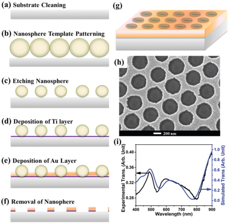
Fig. 2.

A gold nanohole array pattern. (a–g) Protocol for Au nanohole array fabrication; (h) SEM image of a gold nanohole array with a hole diameter of 420 nm at a pitch of 600 nm, and a film thickness of 50 nm; (i) experimentally measured (black curve) and FDTD simulated (blue curve) transmission of the Au nanohole array.
