Abstract
In this work, we report lateral heterojunction formation in as-exfoliated MoS2 flakes by thickness modulation. Kelvin probe force microscopy is used to map the surface potential at the monolayer-multilayer heterojunction, and consequently the conduction band offset is extracted. Scanning photocurrent microscopy is performed to investigate the spatial photocurrent response along the length of the device including the source and the drain contacts as well as the monolayer-multilayer junction. The peak photocurrent is measured at the monolayer-multilayer interface, which is attributed to the formation of a type-I heterojunction. The work presents experimental and theoretical understanding of the band alignment and photoresponse of thickness modulated MoS2 junctions with important implications for exploring novel optoelectronic devices.
Semiconducting transition metal dichalcogenides (TMDCs) with a layered crystal structure exhibit unique electrical1,2 and optical properties3,4,5. TMDCs provide opportunities in exploring new device concepts given their atomic level flatness, and ability to form van der Waals (vdW) heterostructures with strong interlayer coupling6,7,8. For instance, vdW heterobilayers of MoS2/WSe2 have been recently reported to exhibit spatially direct light absorption but spatially indirect light emission, representing a highly intriguing material property9,10. Here, we explore the optoelectronic properties of lateral “hetero”-junctions formed on a single crystal of MoS2 of varying thickness (i.e., number of layers). As a result of the quantum confinement effect11, when the thickness of a MoS2 crystal is scaled down to a monolayer the optical band gap increases from 1.29 eV (indirect) to 1.85 eV (direct)12,13. The change in the band structure and the electron affinity of MoS2 with layer number opens up the path to the formation of atomically sharp heterostructures, not by changing composition but rather by changing layer thickness14. We experimentally examine the surface potential of this thickness modulated heterojunction by using Kelvin probe force microscopy (KPFM). We further use scanning photocurrent microscopy (SPCM) to probe the photoresponse of the junction. A large photocurrent response is observed at the monolayer/multilayer junction interface which confirms the presence of a strong built-in electric field at the interface. Device modeling is used in parallel to experiments to understand the underlying mechanism of the observed photocurrents and the band-alignments at the junction interface, suggesting the formation of a type-I heterojunction.
SPCM has been previously used to study the photoresponse of metal contacted MoS2 transistors, where the channel thickness for MoS2 was uniform throughout the device15,16. The results have shown that the photoresponse is primarily driven by the metal/MoS2 Schottky contacts and photothermoelectric effect16. In distinct contrast to previous studies, we observe that the peak photoresponse is spatially located at the MoS2 monolayer/multilayer junction for our lateral heterojunctions and not at the metal contacts.
Results
Band offset extraction at the monolayer-multilayer MoS2 junction
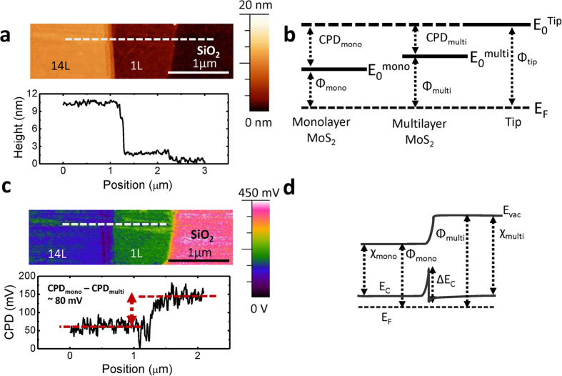
KPFM is performed to spatially map the surface potential, and shed light on the band offsets at the monolayer-multilayer interface. The sample surface topography and contact potential difference (CPD) between the tip and sample are measured simultaneously17,18. Figure 1a demonstrates a monolayer-multilayer junction flake with 10 nm of multilayer (~14 layers; 14 L) thickness. In this particular flake, monolayer to multilayer transition occurs across ~100 nm of the lateral distance in a terraced manner. KPFM is performed using a Bruker MultiMode atomic force microscope under ambient conditions. A Si cantilever tip coated with Pt-Ir (SCM-PIT, Bruker Co.) is used in the tapping mode. Electrical contacts to the MoS2 flake were grounded during the measurements. An AC voltage of 2 V is applied to the tip while the tip height is kept constant at 5 nm. The measured DC voltage of the tip, corresponding to CPD, determines the work function difference between the AFM tip (Pt-Ir) and each region of the MoS2 flake19,20, i.e.,  for the monolayer side and
  for the multilayer side. Φmono, Φmultilayer, and Φtip are the work functions of monolayer MoS2, multilayer MoS2 and the surface of AFM tip, respectively (Fig. 1b). The measured surface potential difference,
  , corresponds to the band bending in the vacuum level Evac at thermal equilibrium, and is also equal to the workfunction difference between the monolayer and the multilayer (Fig. 1b). KPFM map of a representative 1 L–14 L flake is shown in Fig. 1c. From KPFM measurements, the workfunction difference is found to be ~80 meV (Fig. 1c)21,22. Next, we focus on obtaining the energy band diagram for the heterojunction by first extracting the conduction band offset at the interface. The conduction band offset
  at the heterojunction corresponds to the electron affinity difference between the monolayer (χmono) and multilayer (χmultilayer). The workfunction difference between monolayer and multilayer is related to effective density of states (NC),
  and doping levels (ND) as shown in Eq. 1. Here, k is the Boltzmann constant and T is the temperature.
Figure 1.
a. Atomic Force Microscope (AFM) image of a monolayer-multilayer MoS2 flake. b. Representative energy band diagrams of isolated monolayer and multilayer MoS2 with respect to the AFM tip, depicting CPD and work function values. c. Kelvin Force Probe Microscope (KPFM) image of a representative 1L-14L MoS2 flake. d. Representative band diagram of a monolayer-multilayer device at equilibrium.
 |
Boltzmann approximation is considered while deriving Eq. 1. Next we assume the doping level per unit volume is identical in both monolayer and multilayer flakes. Thus Eq. 1 becomes,
 |
Φmulti−mono is measured from KPFM, effective mass values for electrons are taken to be m*n,mono = 0.407 m0 and m*n,multi = 0.574 m0. From these parameters, ∆EC of ~70 meV at the 1 L–14 L interface is extracted. This band offset corresponds to a type-I heterojunction as depicted in the qualitative band diagram of Fig. 1d. Note that the relative values of the dielectric constant of monolayer and multilayer MoS2 determine the electric fields and hence the band bending on both sides of the heterojunction. The dielectric constants are assumed to be the same (~4) in this work24.
Photoresponse at the monolayer-multilayer MoS2 junction
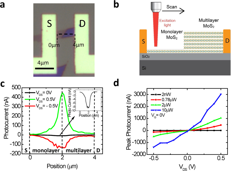
Scanning photocurrent microscopy (SPCM), a spatially resolved photodetection technique that combines electrical measurement and local illumination with a focused laser beam is used to probe the local photoresponse of the monolayer-multilayer MoS2 devices25,26,27,28,29,30. Optical image of a representative device is shown in Fig. 2a. Here, the device consists of a 1 L–5 L MoS2 junction. The channel lengths for the monolayer and the multilayer regions are ~2 μm each. The contact to the monolayer is defined as the source electrode and is electrically grounded. The contact to the multilayer MoS2 serves as the drain electrode to which an external voltage, VDS is applied during the measurements. The heavily doped Si substrate serves as the global back-gate to which voltage, VG can be applied to modulate the electric potential in MoS2. The device is locally illuminated by a focused laser beam (wavelength: 488 nm, diameter: ~1 μm) as depicted in Fig. 2b. The spatial resolution of the scanning stage is 0.1 μm. The light current, Ilight is recorded as the laser spot is scanned across the length of the device. The photocurrent, Iphotocurrent, is then obtained as a function of illumination spot by subtracting the dark current of the device, Idark, from Ilight. In contrast to previous reports studying the photoresponse in MoS2 single layer or multilayer devices (Fig. S2)3,15,16,31, the peak photocurrent in our device is observed at the monolayer-multilayer interface rather than the metal/semiconductor junction. Figure 2c shows the spatial response of the photocurrent along the dashed line of Fig. 2a at VG = 0 V and laser intensity of 0.78 μW. Source-drain voltage is varied from −0.5 V to 0.5 V. Even without source drain bias (VDS = 0 V), a finite short circuit current (~8 nA) is measured as seen in the inset of Fig. 2c. This implies that the expected band bending and the resulting built-in electric field that is induced by the difference in the electron affinities of the monolayer and multilayer MoS2 regions is capable of separating the electron-hole pairs generated at the monolayer-multilayer interface. The dependence of the photocurrent on VDS and the excitation power is investigated to further characterize the monolayer-multilayer junction devices. The peak photocurrent, corresponding to the local illumination of the monolayer-multilayer interface, is measured at different illumination intensities of 2 nW, 0.78 μW, 2 μW and 10 μW and VDS of −0.5 V to 0.5 V at VGS = 0 V (Fig. 2d). The photocurrent increases as the applied VDS bias is increased due to the contribution of the enhanced drift current and decreased transit time of the electrons3. The increase in the photocurrent with the illumination can be attributed to generation of higher number of electron-hole pairs. It is important to note that at all different laser powers and VDS values the peak photocurrent response is observed at the monolayer-multilayer heterojunction.
Figure 2.
a. Optical microscope image of the monolayer-multilayer device with Ni/Au (30 nm/30 nm) contacts. b. Schematic representation of the SPCM measurement. c. Photoresponse of the monolayer-multilayer MoS2 flake versus position along the dashed line at VG = 0 V, with illumination power of 0.78 μW and with VDS = −0.5 V, VDS = 0.5 V and VDS = 0 V. d. Peak photocurrent vs. VDS at VGS = 0 V with different illumination powers.
Photoresponsivity at the monolayer-multilayer MoS2 junction
To further characterize the photocurrent generation at the heterojunction, photoresponsivity is experimentally investigated as a function of VDS and laser power. Photoresponsivity determines the gain of a photodetector system in terms of the ratio of photocurrent generated (Iphotocurrent) and the incident laser power (Pincident), i.e., (Iphotocurrent) / Pincident. Figure 3a shows the photoresponsivity with varying laser powers at VG = 0 V. It is found to increase as the VDS increases from 0 V to 0.5 V. The maximum photoresponsivity is found to be 580 mA / W at VDS = 0.5 V and with the power of 0.78 μW. Given the power of the laser (0.78 μW) and the VDS value of 0.5 V and at VG = 0 V, the maximum photoresponsivity of the monolayer – multilayer heterojunction is found to be greater than the highest reported MoS2 photodetector in the literature3,15,31,32. Moreover, the dependence of the photocurrent on power is investigated. Figure 3b shows a linear relationship between the peak photocurrent and the laser power. This is consistent with the response of standard photodiodes where the photocurrent is proportional to the carrier generation rate and hence the light intensity33.
Figure 3.
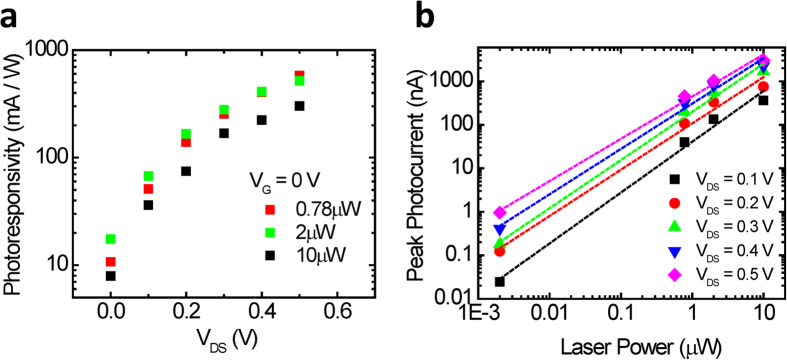
a. Photoresponsivity vs. the applied VDS at VG = 0 V and with different laser power. b. Peak photocurrent vs. laser power at VG = 0 V and at different VDS values.
Dependence of the peak photocurrent on the gate bias
Next, we explore the effect of gate voltage on the peak photocurrent. Figure 4a shows the measured photocurrent as a function of displacement along the length of the device for VGS ranging from −30 V to 30 V. The drain voltage is maintained constant at 1 V with an illumination power of 2 μW. The effect of gate voltage on the photocurrent is minimal. This is further illustrated in Fig. 4b where the peak photocurrent is plotted as a function of gate voltage. For comparison the dark current as a function of gate voltage for the same device is also shown. While the dark current shows strong gate dependency, consistent with n-type characteristics of MoS2, the light current exhibits nearly no gate dependence. This is distinct from the previous studies of photocurrent for a uniform thickness MoS2 flake, where the gate voltage was shown to modulate the Schottky barrier heights and thus the photoresponse34. In contrast, the peak photocurrent in our devices arise from the monolayer-multilayer junction where the global back-gate has minimal effect on its potential profile.
Figure 4.
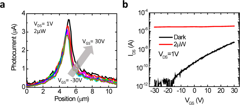
a. Photocurrent vs. position at VDS = 1 V with illumination power of 2 μW and VGS varied from −30 V to 30 V at 10 V increments. b. IDS vs. VGS at VDS = 1 V in dark and with 2 μW of illumination power.
Discussion
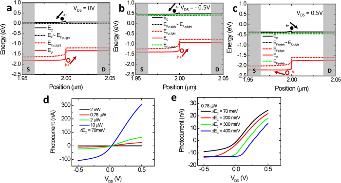
Device modeling was performed using TCAD Sentaurus to further understand the junction properties for a monolayer-multilayer device. For the Sentaurus simulations a ∆EC ~ 70 meV, calculated from the KPFM data is used. The doping level for both monolayer and multilayer regions are assumed to be ND,mono = ND,multi = 1018 cm−3,35. The effect of the back gate is modeled as a change in the device doping concentration. The effective mass values are taken to be m*e ~ 0.407 m0 for the monolayer and m*e ~ 0.574 m0 for the multilayer as described earlier23. The dielectric constants are assumed to be the same εmono = εmultilayer = 4 ε023. For the simulated device, the exact dimensions of the measured device presented in Fig. 2 are used. Electron affinities are assumed to be χmonolayer = 4 eV36 and χmultilayer = 4.07 eV, such that ∆EC = 70 meV as obtained earlier using the experimental KPFM data. Measured values for bandgap of monolayer (1.85 eV) and 5 layers (1.4 eV) are used12. A light window of 1 μm is used that corresponds to the spot size of the laser and is shined in the center of the junction. A laser wavelength of 488 nm and an absorption coefficient of 106 cm−1 for the monolayer and 105 cm−1 for the multilayer side is assumed for the simulations15,37. Thus with the assumptions stated above and using the KPFM information, simulations revealed a type – I heterojunction band alignment in the monolayer – multilayer MoS2 heterojunction flake as seen in Fig. 5a–c.
Figure 5. Simulated band diagrams at.
a, VDS = 0 V, b, VDS = −0.5 V and c, VDS = 0.5 V in dark and with light shined at the monolayer – multilayer MoS2 junction. d. Simulated photocurrent vs. VDS at different laser powers. e. Simulated photocurrent vs. VDS with different ∆EC values.
Figure 5a shows the simulated band diagram at VDS = 0 V for the dark condition and when light is illuminated at the monolayer-multilayer interface. Under illumination, Fermi levels split (EF,n and EF,p) as a result of the generation of the electron hole pairs. At a simulated laser power of 0.78 μW, low level injection conditions prevail and no change in the quasi Fermi level for electrons is observed as seen in Fig. 5a. At zero VDS bias, due to the built-in electric field at the heterojunction, electrons that are generated at the monolayer side of the monolayer-multilayer junction are swept to the monolayer side (source). However electrons generated at the multilayer side are subjected to a barrier height of 70 meV. Holes do not encounter any barrier and freely move to the multilayer side (drain). This is consistent with the measured SPCM data, where a negative photocurrent of 8 nA is recorded at zero VDS signifying that the electrons are collected at the source (monolayer) and holes at the drain (multilayer) side.
Previous studies have shown small Schottky barrier heights for electrons both in monolayer and multilayer MoS2, on the order of 200 meV or less38,39,40,41. The barrier height for electrons at the monolayer-multilayer interface is ∆EC = 70 meV as calculated. In this system, the Schottky barrier height at the contacts and the barrier height at the junction are on the same order of magnitude. Therefore a part of the applied VDS gets dropped at the contacts, and the remaining voltage is dropped at the monolayer-multilayer MoS2 interface. When a negative VDS (Fig. 5b) is applied to the multilayer side (drain), there is a higher built-in electric field and a wider depletion region at the junction. A wider depletion region at the monolayer side allows the separation of a larger number of photogenerated electron-hole pairs thus resulting in a larger negative photocurrent compared to the case of zero VDS as the electrons get swept to the monolayer side (source) and holes swept to the multilayer side (drain) freely. However electrons generated at the multilayer side still face a barrier height of ~70 meV, just like in the case of zero bias. By applying a positive VDS (Fig. 5c) the barrier height for electron transport from the monolayer to the multilayer is nearly diminished. Electron-hole pairs generated at the monolayer side contribute to the photocurrent since holes move to the monolayer side (source) freely and electrons can go over the decreased barrier height and move to the multilayer side (drain). Whereas, electron-hole pairs generated at the multilayer side don’t contribute to the photocurrent since holes see a barrier of ΔEV (~0.38 eV). This current flow mechanism is consistent with measuring positive photocurrent at VDS > 0 and measuring negative photocurrent for VDS < 0 as seen in Fig. 2d.
Photocurrent vs. applied VDS is also simulated in TCAD Sentaurus with different illumination intensities. The same parameters and assumptions that are used to generate the band diagrams mentioned above are used to simulate the VDS and the light intensity dependence of the photocurrent. In the SPCM measurements, as seen in Fig. 2c, at VDS = 0 V a negative photocurrent is observed. As the applied bias is increased to VDS = 0.1 V, photocurrent becomes positive (Fig. 2d). This implies that the experimental crossover from the negative photocurrent to positive photocurrent is in between VDS = 0 V and VDS = 0.1 V. The simulated photocurrents are shown in Fig. 5d–e. The simulation is in qualitative agreement with the experimental data, with the transition from the negative to positive photocurrent occurring at positive VDS values. The negative to positive photocurrent crossover voltage is sensitive to the parameter values assumed for the simulations. Figure 5e illustrates the large dependence of the simulated crossover voltage on the ∆EC value. Quantitative differences between the simulated and experimental data can also arise from the presence of a terraced junction as described in Fig. 1a, compared to the ideal step heterojunction simulated in Sentaurus. The Sentaurus simulations however qualitatively explain the experimental data and all the trends, but a quantitative analysis warrants simulations or first principle calculations using exact values of absorption coefficient, electron affinities, effective masses, doping, carrier lifetimes, diffusion lengths, etc.
In conclusion, the type-I heterojunctions enabled by lateral thickness modulation of MoS2 are demonstrated. The junction properties are characterized by KPFM and SPCM. A workfunction difference of 80 meV is measured by KPFM. Furthermore, a conduction band offset of 70 meV is extracted from the difference in the electron affinities and work functions of the monolayer and multilayer regions of the MoS2. Photocurrent generation at the monolayer-multilayer heterojunction is observed with SPCM. The peak photocurrent generation at the monolayer-multilayer junction is attributed to the electric field in the depletion region at the heterojunction formed by the difference in the work functions and the electron affinities of the monolayer and the multilayer flake. A short circuit current of 8 nA is measured due to the built-in electric field being able to separate and collect the generated electron hole pairs at the monolayer-multilayer junction. The photoresponsivity of the monolayer-multilayer MoS2 junction is studied with respect to the incident light power and the source-drain bias. The demonstration of the type-I heterojunction on the same MoS2 flake will inspire further investigation regarding the electronic transport properties of the atomically sharp type-I band alignment in the TMDC flakes.
Methods
The fabrication process for thickness modulated MoS2 heterojunction devices is as follows. MoS2 crystals (SPI Supplies) are transferred onto Si/SiO2 (260 nm thick) substrates using the micromechanical exfoliation technique. The flakes of interest consisting of mono-multilayer junctions are identified using an optical microscope. These flakes are formed naturally during the exfoliation process. In order to verify the thicknesses of the mono-multilayer regions, atomic force microscopy (AFM) is performed (Fig. 1a). Monolayer thickness of 0.7 nm is confirmed1 and a multilayer thicknesses ranging from 6–15 nm is measured for the different samples explored in this study. Photoluminescence (PL) mapping of the flakes was conducted to further depict the mono- and multi-layer regions using a 532 nm pump laser with 8–80 μW power and a spot size of ∼0.5 μm (Horiba Scientific LabRAM HR 800). PL map of a representative flake is shown in Fig. S1c, where the luminescence signal ratio is approximately one order of magnitude between the two regions of the MoS2, further depicting the formation of a thickness modulated heterojunction. Metal source/drain (S/D) contacts are subsequently formed with one contact on the monolayer region and the other on the multilayer region of the MoS2 flake. Electron-beam lithography was used to pattern the metal contacts, followed by evaporation of Ni/Au (30/30 nm), and lift-off of the resist in acetone.
Additional Information
How to cite this article: Tosun, M. et al. MoS2 Heterojunctions by Thickness Modulation. Sci. Rep. 5, 10990; doi: 10.1038/srep10990 (2015).
Supplementary Material
Acknowledgments
This work was funded by the Director, Office of Science, Office of Basic Energy Sciences, Material Sciences and Engineering Division of the U.S. Department of Energy under Contract No. DE-AC02-05CH11231. The device fabrication and characterization was funded by the Center for Low Energy Systems Technology (LEAST), one of six centers supported by the STARnet phase of the Focus Center Research Program (FCRP), a Semiconductor Research Corporation program sponsored by MARCO and DARPA.
Footnotes
Author Contributions M.T., D.F. and A.J. designed the experiments. M.T., D.F., J.S.K., D.H.L. and C.K. carried out the experiments, S.B.D. performed the TCAD Sentaurus simulations. M.T., D.F., S.B.D., C.K., M.N., S.T., J.W. and A.J. contributed to the data analysis. M.T., S.B.D. and A.J., wrote the paper while all authors provided feedback.
References
- Radisavljevic B., Radenovic A., Brivio J., Giacometti V. & Kis A. Single-layer MoS2 transistors. Nat Nano. 6, 147–150 (2011). [DOI] [PubMed] [Google Scholar]
- Fang H. et al. High-Performance Single Layered WSe2 p-FETs with Chemically Doped Contacts. Nano Lett. 12, 3788–3792 (2012). [DOI] [PubMed] [Google Scholar]
- Lopez-Sanchez O., Lembke D., Kayci M., Radenovic A. & Kis A. Ultrasensitive photodetectors based on monolayer MoS2. Nat Nano. 8, 497–501 (2013). [DOI] [PubMed] [Google Scholar]
- Baugher B. W. H., Churchill H. O. H., Yang Y. & Jarillo-Herrero P. Optoelectronic devices based on electrically tunable p-n diodes in a monolayer dichalcogenide. Nat Nano. 9, 262–267 (2014). [DOI] [PubMed] [Google Scholar]
- Ross J. S. et al. Electrically tunable excitonic light-emitting diodes based on monolayer WSe2 p-n junctions. Nat Nano. 9, 268–272 (2014). [DOI] [PubMed] [Google Scholar]
- Cheng R. et al. Electroluminescence and Photocurrent Generation from Atomically Sharp WSe2/MoS2 Heterojunction p–n Diodes. Nano Lett. 14, 5590–5597 (2014). [DOI] [PMC free article] [PubMed] [Google Scholar]
- Gong Y. et al. Vertical and in-plane heterostructures from WS2/MoS2 monolayers. Nat Mater. 13, 1135–1142 (2014). [DOI] [PubMed] [Google Scholar]
- Furchi M. M., Pospischil A., Libisch F., Burgdörfer J. & Mueller T. Photovoltaic Effect in an Electrically Tunable van der Waals Heterojunction. Nano Lett. 14, 4785–4791 (2014). [DOI] [PMC free article] [PubMed] [Google Scholar]
- Fang H. et al. A. Strong interlayer coupling in van der Waals heterostructures built from single-layer chalcogenides. Proc. Natl. Acad. Sci. USA 111, 6198–6202 (2014). [DOI] [PMC free article] [PubMed] [Google Scholar]
- Lee C.-H. et al. Atomically thin p–n junctions with van der Waals heterointerfaces. Nat Nano. 9, 676–681 (2014). [DOI] [PubMed] [Google Scholar]
- Kuc A., Zibouche N. & Heine T. Influence of quantum confinement on the electronic structure of the transition metal sulfide. Phys. Rev. B. 83, 245213 (2011). [Google Scholar]
- Mak K. F., Lee C., Hone J., Shan J. & Heinz T. F. Atomically Thin MoS2: A New Direct-Gap Semiconductor. Phys. Rev. Lett. 105, 136805 (2010). [DOI] [PubMed] [Google Scholar]
- Splendiani A. et al. Emerging Photoluminescence in Monolayer MoS2. Nano Lett. 10, 1271–1275 (2010). [DOI] [PubMed] [Google Scholar]
- Howell S.L. et al. Investigation of Band-Offsets at Monolayer–Multilayer MoS2 Junctions by Scanning Photocurrent Microscopy. Nano Lett. 15, 2278–2284 (2015). [DOI] [PubMed] [Google Scholar]
- Wu C.-C. et al. Elucidating the Photoresponse of Ultrathin MoS2 Field-Effect Transistors by Scanning Photocurrent Microscopy. J. Phys. Chem. Lett. 4, 2508–2513 (2013). [Google Scholar]
- Buscema M. et al. Large and Tunable Photothermoelectric Effect in Single-Layer MoS2. Nano Lett. 13, 358–363 (2013). [DOI] [PubMed] [Google Scholar]
- Wang X., Xie W., Chen J. & Xu J.-B. Homo- and Hetero- p–n Junctions Formed on Graphene Steps. ACS Appl. Mater. Interfaces. 6, 3–8 (2013). [DOI] [PubMed] [Google Scholar]
- Ko C., Yang Z. & Ramanathan S. Work Function of Vanadium Dioxide Thin Films Across the Metal-Insulator Transition and the Role of Surface Nonstoichiometry. ACS Appl. Mater. Interfaces. 3, 3396–3401 (2011). [DOI] [PubMed] [Google Scholar]
- Nonnenmacher M., O’Boyle M. P. & Wickramasinghe H. K. Kelvin probe force microscopy. Appl. Phys. Lett. 58, 2921–2923 (1991). [Google Scholar]
- Melitz W., Shen J., Kummel A. C. & Lee S. Kelvin probe force microscopy and its application. Surf. Sci. Rep. 66, 1–27 (2011). [Google Scholar]
- Ochedowski O. et al. Effect of contaminations and surface preparation on the work function of single layer MoS2. Beilstein J. Nanotechnol. 5, 291–297 (2014). [DOI] [PMC free article] [PubMed] [Google Scholar]
- Choi S., Shaolin Z. & Yang W. Layer-number-dependent work function of MoS2 nanoflakes. J. Korean Phys. Soc. 64, 1550–1555 (2014). [Google Scholar]
- Zahid F., Liu L., Zhu Y., Wang J. & Guo H. A generic tight-binding model for monolayer, bilayer and bulk MoS2. AIP Adv. 3, 052111 (2013). [Google Scholar]
- Santos E. J. G. & Kaxiras E. Electrically Driven Tuning of the Dielectric Constant in MoS2 Layers. ACS Nano. 7, 10741–10746 (2013). [DOI] [PubMed] [Google Scholar]
- Miller C. et al. Unusually long free carrier lifetime and metal-insulator band offset in vanadium dioxide. Phys. Rev. B. 85, 085111 (2012). [Google Scholar]
- Balasubramanian K., Burghard M., Kern K., Scolari M. & Mews A. Photocurrent Imaging of Charge Transport Barriers in Carbon Nanotube Devices. Nano Lett. 5, 507–510 (2005). [DOI] [PubMed] [Google Scholar]
- Gu Y., Romankiewicz J. P., David J. K., Lensch J. L. & Lauhon L. J. Quantitative Measurement of the Electron and Hole Mobility−Lifetime Products in Semiconductor Nanowires. Nano Lett. 6, 948–952 (2006). [Google Scholar]
- Graham R., Miller C., Oh E. & Yu D. Electric Field Dependent Photocurrent Decay Length in Single Lead Sulfide Nanowire Field Effect Transistors. Nano Lett. 11, 717–722 (2010). [DOI] [PubMed] [Google Scholar]
- Fu D. et al. Electrothermal Dynamics of Semiconductor Nanowires under Local Carrier Modulation. Nano Lett. 11, 3809–3815 (2011). [DOI] [PubMed] [Google Scholar]
- Yu D. & Graham R. Scanning Photocurrent Microscopy in Semiconductor Nanostructures. Mod. Phys. Lett. B. 27, 1330018 (2013). [Google Scholar]
- Yin Z. et al. Single-Layer MoS2 Phototransistors. ACS Nano. 6, 74–80 (2011). [DOI] [PubMed] [Google Scholar]
- Esmaeili-Rad M. R. & Salahuddin S. High Performance Molybdenum Disulfide Amorphous Silicon Heterojunction Photodetector. Sci. Rep. 3, 2345; 10.1038/srep02345 (2013). [DOI] [PMC free article] [PubMed] [Google Scholar]
- Sze S. M. Semiconductor devices, physics and technology. [668–669] (Wiley, New Jersey, 2007). [Google Scholar]
- Li H.-M. et al. Metal-Semiconductor Barrier Modulation for High Photoresponse in Transition Metal Dichalcogenide Field Effect Transistors. Sci. Rep. 4, 4041; 10.1038/srep04041 (2014). [DOI] [PMC free article] [PubMed] [Google Scholar]
- Fang H. et al. Degenerate n-Doping of Few-Layer Transition Metal Dichalcogenides by Potassium. Nano Lett. 13, 1991–1995 (2013). [DOI] [PubMed] [Google Scholar]
- Kang J., Liu W., Sarkar D., Jena D. & Banerjee K. Computational Study of Metal Contacts to Monolayer Transition-Metal Dichalcogenide Semiconductors. Phys. Rev. X. 4, 031005 (2014). [Google Scholar]
- Bernardi M., Palummo M. & Grossman J. C. Extraordinary Sunlight Absorption and One Nanometer Thick Photovoltaics Using Two-Dimensional Monolayer Materials. Nano Lett. 13, 3664–3670 (2013). [DOI] [PubMed] [Google Scholar]
- Das S., Chen H.-Y., Penumatcha A. V. & Appenzeller J. High Performance Multilayer MoS2 Transistors with Scandium Contacts. Nano Lett. 13, 100–105 (2012). [DOI] [PubMed] [Google Scholar]
- Kaushik N. et al. Schottky barrier heights for Au and Pd contacts to MoS2. Appl. Phys. Lett. 105, 113505 (2014). [Google Scholar]
- Amani M. et al. Growth-substrate induced performance degradation in chemically synthesized monolayer MoS2 field effect transistors. Appl. Phys. Lett. 104, 203506 (2014). [Google Scholar]
- Kang J., Liu W. & Banerjee K. High-performance MoS2 transistors with low-resistance molybdenum contacts. Appl. Phys. Lett. 104, 093106 (2014). [Google Scholar]
Associated Data
This section collects any data citations, data availability statements, or supplementary materials included in this article.


