Abstract
The integration of ultra-thin gate oxide, especially at sub-10 nm region, is one of the principle problems in MoS2 based transistors. In this work, we demonstrate sub-10 nm uniform deposition of Al2O3 on MoS2 basal plane by applying ultra-low energy remote oxygen plasma pretreatment prior to atomic layer deposition. It is demonstrated that oxygen species in ultra-low energy plasma are physically adsorbed on MoS2 surfaces without making the flakes oxidized, and is capable of benefiting the mobility of MoS2 flake. Based on this method, top-gated MoS2 transistor with ultrathin Al2O3 dielectric is fabricated. With 6.6 nm Al2O3 as gate dielectric, the device shows gate leakage about 0.1 pA/μm2 at 4.5 MV/cm which is much lower than previous reports. Besides, the top-gated device shows great on/off ratio of over 108, subthreshold swing (SS) of 101 mV/dec and a mobility of 28 cm2/Vs. With further investigations and careful optimizations, this method can play an important role in future nanoelectronics.
Transition metal dichalcogenides are a family of layered structure materials that could be used for next-generation nanoelectronic devices1,2,3,4,5. Stable few-layer and single-layer flakes can be obtained by the classical mechanical exfoliation which was initially used for graphene. In contrast with zero-band gap graphene, bulk MoS2 is a semiconductor with an indirect band gap of 1.29 eV while monolayer MoS2 has a direct band gap of 1.8 eV6,7. Furthermore, because of its ultrathin nature, single-layer MoS2 transistors are advantageous in nanometer-scale metal oxide semiconductor field-effect transistors (MOSFETs) as they are immune to short-channel effects8. These advantages make MoS2 suitable for future complementary metal oxide semiconductor (CMOS)-like logic device applications.
Excellent performance of MoS2 transistors adopted back gate structure have been demonstrated widely9,10,11. Furthermore, dual gate and top gate MoS2 based transistors with high-κ dielectrics have also attracted much attention recently. Since it enables the individual control of each device, the realization of high-performance dual gate or top-gated MoS2 transistors is a necessary step towards the practical application1,8,12,13,14,15,16,17,18. However, there are still some difficulties in the integration of high-κ dielectrics on MoS2 surfaces. Even though uniform atomic layer deposition (ALD) process of Al2O3 on MoS2 at 200 °C has been reported by Liu et al.19, leading to the suggestion that direct nucleation of precursors on MoS2 may be feasible, other works have shown that with pristine MoS2 flakes the direct deposition of high-κ dielectrics form island-like clusters, owing to the absence of dangling bonds on MoS2 basal plane20,21. It might be the use of organic pre-cleaning steps that led to uniform deposition of Al2O3 at 200 °C in Liu’s work19. In addition, it was observed in this work that within the measurement range, neither the growth temperature nor the pulse time had an obvious impact on the topography of the Al2O3 layer grown on MoS2 flakes. The island-like growth of high-κ dielectrics on MoS2 would induce a large leakage current, therefore top-gated high-κ dielectrics in nearly all the previous reports are very thick and MoS2 transistors with sub-10 nm top gate dielectrics are seldom reported1,8,12,13,14,15,16,17,18. For example, in recent reports, the top gate dielectrics of MoS2 transistors are 50 nm Al2O316 and 30 nm HfO218 for the work by Pezeshki A. et al. and Krasnozhon D. et al., respectively. Only by realizing high-quality pinhole-free and thin dielectrics over large area on MoS2 can the continual scaling down of MoS2 FETs be possible. With the shrink of dielectric thickness, especially at sub-10 nm region, the gate capacitance would be greatly improved, leading to better control of the channel and larger drive current. Some methods have been proposed to achieve uniform growth of high-κ materials on MoS2, such as an ultrathin metal oxide buffer layer, organic functionalization of MoS2 and ultraviolet-ozone exposure20,21,22. But most of the work just stopped at the early stage of realizing uniform growth without exploring the impacts of surface functionalization on devices performance, especially on gate leakage.
In this work, a CMOS process compatible method to achieve uniform Al2O3 growth on MoS2 basal plane by applying a remote O2 plasma treatment prior to Al2O3 growth is proposed, and top-gated MoS2 MOSFET with ultrathin Al2O3 dielectric deposited using this method is also studied. Notably, the Al2O3 dielectric layer is about 6.6 nm, which is the thinnest top gate dielectric ever reported, but exhibits the impressive leakage current about 0.1 pA/μm2 at 4.5 MV/cm. This leakage is even much smaller than that of MoS2 transistors capped with much thicker top gate dielectrics1,8,13,16,17. At the same time, the top-gated device also shows great on/off ratio of over 108, subthreshold swing (SS) of 101 mV/dec and a mobility of 28 cm2/Vs. In addition, mechanism investigations show that after the pretreatment, oxygen atoms are physically adsorbed on the MoS2 surface without oxidizing it. This non-destructive physical adsorption mechanism is revealed by the advanced ultra-high-vacuum (UHV) in-situ analysis system. We believe it will benefit the two-dimensional electronic devices research a lot.
Results
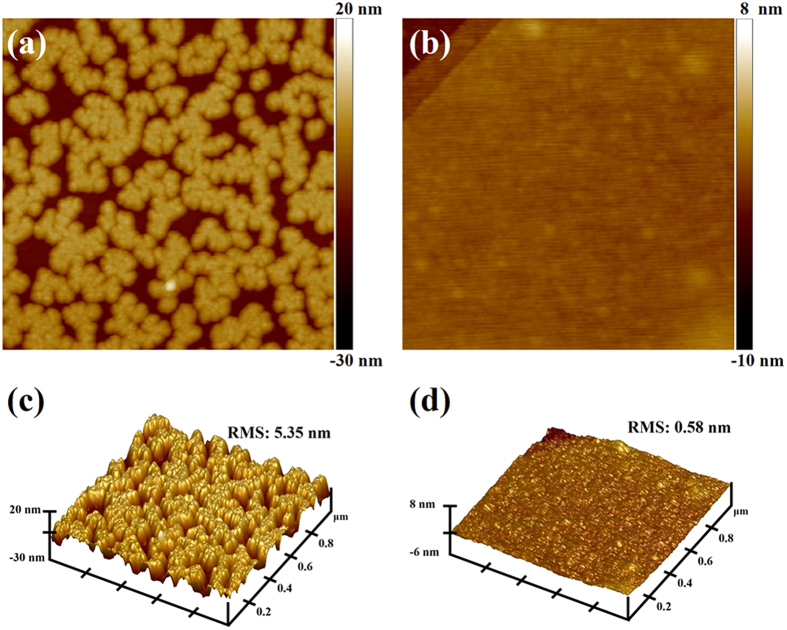
Leakage current of gate oxide results in high power consumption and performance degradation of the two dimensional layered transistors20. To achieve uniform ALD Al2O3 growth on pristine MoS2, functionalization of the MoS2 surface is required to introduce uniform surface groups that serve as active nucleation sites for the ALD process21,23. Initially, an investigation on few-layer MoS2 flakes was carried out with a plasma enhanced ALD system. For the sample in Fig. 1a, 120 cycles Al2O3 was directly deposited on MoS2 surface at 200 °C using TMA (Trimethyl Aluminum) and H2O as precursors, which were kept at 18 °C in stainless bottles. By comparison, the sample in Fig. 1b was exposed to a low energy remote O2 plasma treatment before ALD. The pretreatment contained two steps. Each step consisted of 30 s remote O2 plasma exposure followed by purging with Ar for 5 s. Afterwards, 120 cycles Al2O3 was deposited in the same chamber. The different growth topography of Al2O3 on MoS2 basal planes are shown in Fig. 1. From Fig. 1a, it can be seen that due to the absence of dangling bonds on MoS2 basal plane, direct deposition of Al2O3 films are in forms of island-like clusters with large pinholes, and the lateral size of most pinholes are over 100 nm. In this situation, it is easy to imagine that the gate dielectric of top gate MoS2 transistors have to be thick to form uniform film which is necessary to keep the leakage current at a sufficient lower level. By contrast, with remote oxygen plasma treatment prior to ALD, the grown Al2O3 film is completely uniform on MoS2 surface as shown in Fig. 1b. The difference is even more evident by the comparison between Fig. 1c,d, which are the corresponding AFM 3D images of Fig. 1a,b. Root mean square (RMS) of the ~12 nm directly deposited film is 5.35 nm, and it decreases to only 0.58 nm with remote oxygen plasma pretreatment, which is about 10% of the value in Fig. 1c. It is obvious that the remote O2 plasma pretreatment served as an effective method to supply sufficient nucleation sites to achieve a uniform ALD process. More details about the direct deposition of Al2O3 on pristine MoS2 basal planes are available in the Supplementary Information. According to previous reports with graphene24 and MoS225,26, heavy exposure to an oxygen plasma (typically a direct plasma) completely etches the flakes and results in the substitution of sulfur with oxygen and re-deposition of the surface materials during etching of the MoS2 flakes. Therefore, further analysis is needed to investigate the impact of the low energy remote oxygen plasma.
Figure 1. AFM images after 120 Al2O3 cycles at 200 °C.
(a) Direct growth of the Al2O3 films on MoS2 flakes. (b) The remote O2 plasma pretreatment performed before ALD. (c,d) are the corresponding 3D images of (a,b), respectively. The scan size for all of the images is 1 μm by 1 μm.
In-situ investigations were performed to gain an insight into the mechanisms of uniform growth after a remote O2 plasma pretreatment, looking at whether the MoS2 flakes were oxidized during the treatment or oxygen atoms were adsorbed on the MoS2 surface and acted as nucleation sites in the following ALD process. In the in-situ cluster system, the ALD system was connected to an X-ray photoelectron spectroscopy (XPS) system through a high-vacuum transfer line (the pressure was about 10−10 mbar). The sample was first transferred from the load-lock chamber to the XPS chamber for characterization. It was then transferred to the ALD chamber for 5 s remote O2 plasma treatment. Afterwards, the sample was transferred back into the XPS chamber for further measurements. This procedure was repeated twice with treatment time of 15 and 30 s. The Mo 3d, S 2s and S 2p regions of the XPS spectra are shown in Fig. 2a,b, respectively. The Mo 3d spectra consists of peaks around 229 and 232 eV, corresponding to the Mo4+ 3d5/2 and Mo4+ 3d3/2 components, respectively. Similar peaks appear around 161.8 and 163 eV, referring to the S 2p3/2 and S 2p1/2 components of the S 2p region, respectively. In Fig. 2, all these peaks have nearly no shift after the remote O2 plasma treatment, implying that the chemical bonds were not damaged during the process. Also, no peaks appear around 236 eV, demonstrating that the molybdenum atoms were not oxidized after the plasma treatment27,28. This is different to the previous results where a direct RF-oxygen plasma was applied25,26,28. Based on the discussion above, it seems that remote oxygen plasma treatment is a surface-based process. When a remote oxygen plasma was applied, oxygen atoms were adsorbed onto the MoS2 surfaces and acted as nucleation sites for the ALD process. The remote plasma was gentle enough such that the flakes were not oxidized during the treatments. When the flakes were transferred into the XPS chamber through the transfer line, the adsorbed oxygen atoms desorbed, caused by the high vacuum in the transfer line and the reductive environment due to the working principle of the molecular pump. In addition, it should be noticed that the intensity of both Mo 3d and S 2p peaks varied with the measurement position actually. As there were a lot of MoS2 flakes on the tested SiO2 substrate, and tiny position shifts between adjacent measurements were inevitable, results obtained from different XPS measurements may contain information from different MoS2 flakes. Meanwhile, since the thickness and density of MoS2 flakes varied according to their locations, there were some intensity differences in both Mo 3d and S 2p components with treatment time. In this case, the intensity of Mo 3d and S 2p components with 5 + 15 s remote oxygen plasma treatment happened to be the maximum.
Figure 2.
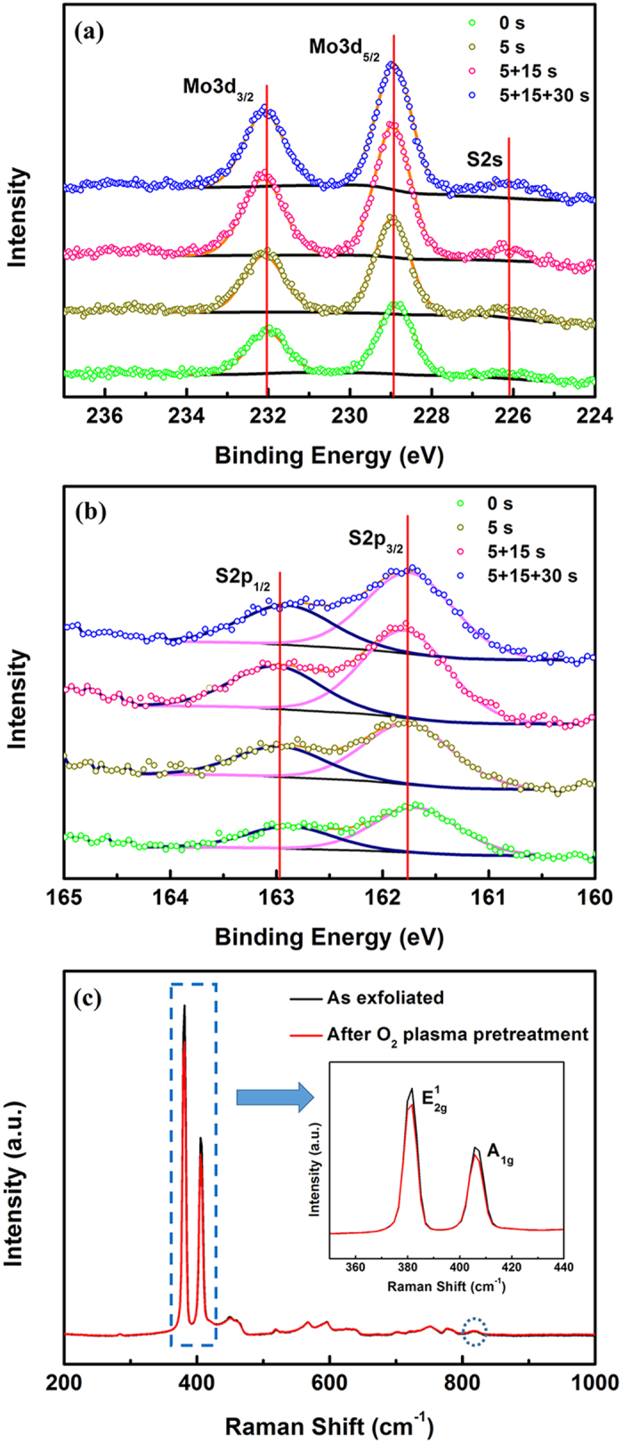
(a) In-situ XPS spectra showing the Mo 3d and S 2s core level peak regions before and after remote O2 plasma treatments for various time. (b) In-situ XPS spectra showing the S 2p core level peak regions. (c) Raman spectra before and after the remote O2 plasma treatments. The inset is a zoom of the spectra showing the  and A1g peaks in MoS2. The blue dotted circle in (c) is used to highlight the peak near 820 cm−1 which is used to estimate the extent of MoS2 oxidation.
To further verify the results obtained by XPS, Raman spectra of the sample before and after the oxygen plasma treatments mentioned above were obtained in air using a 514-nm laser (Fig. 2c). The inset of Fig. 2c displays the spectra enlarged, showing the  and A1g modes for MoS2 at ~380 and 405 cm−1. According to the work of Bertrand P. A.29, the in-plane
  mode is brought about by the opposite vibration of two S atoms with respect to a Mo atom and the A1g mode is generated from the out-of-plane vibration of S atoms in opposite directions. From the inset of Fig. 2c, consistency of peak positions between these two spectra at the
  and A1g modes can be observed before and after the sample undergoing the remote oxygen plasma treatments, implying that bonding situations of Mo and S atoms didn’t change. In addition, the peak that centers near 820 cm−1 could be used to estimate the extent of oxidation that occurred30. In case that the MoS2 flakes were oxidized, this peak would be more defined and intense after the treatments. As expected, this peak showed no intensity difference before and after the remote O2 plasma pretreatments, indicating that the MoS2 flakes remained un-oxidized during the pretreatments. From these results, it is clear that during the treatments, the remote O2 plasma is gentle enough to avoid damaging the MoS2 flakes. Instead, the produced oxygen species are adsorbed onto the MoS2 surface and serve as nucleation sites for the initial TMA pulses during the ALD process.
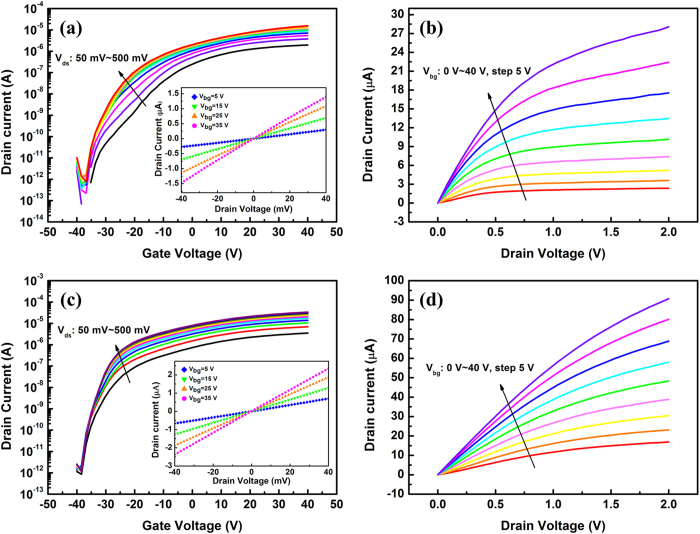
As the mobility is of great significance when evaluating the performance of electronic devices, back-gated MoS2-based field effect transistors were fabricated to estimate the impact of the remote O2 plasma pretreatment on the device mobility. A cross-sectional schematic of the MoS2 transistor with the remote O2 plasma treatment is shown in Fig. 3a, and thickness of the MoS2 flake is about 8.4 nm as shown in Fig. 3b, which correspond to ~12 monolayers. The corresponding photograph of the device structure is shown in Fig. 3c. For the electrical characterization, one of the electrodes acts as a drain and the other one is grounded, acting as a source. Initially, Cr/Au electrodes are used with a MoS2 channel by applying a source-drain bias (Vds) to the pair of electrodes as shown in Fig. 3c and a gate bias (Vbg) to the heavily doped silicon substrate. As shown in the insets in Fig. 4a,c, the Ids – Vds curves are all linear in the range from −40 to 40 mV with or without the remote O2 plasma pretreatment, indicating that the Cr/Au contacts are ohmic contacts. The transfer and output characteristics for the MoS2 transistor before and after 60 s remote O2 plasma pretreatment are obtained for comparison. The data presented in Fig. 4 show typical n-type transistor behavior with an on/off ratio (Ion/Ioff) over 107. This high on/off ratio compared to graphene transistors is attributed to the large band gap of MoS2. It is also observed in Fig. 4a,c that both the shape of the transfer curves and the values of the ON current are improved after 60 s remote O2 plasma pretreatment. For example, the transfer current at Vds = 500 mV increases from 1.56 × 10⁻⁵ to 3.38 × 10⁻⁵ A after a 60 s remote O2 plasma pretreatment. A low field-effect mobility is extracted using the Equation:[1]
 |
where L = 1 μm is the channel length, W = 4.2 μm is the channel width, and Ci = 1.15 × 10⁻⁸ F/cm2 is the capacitance density between the channel and the back gate (details of the mobility extraction can be found in Supplementary Information). Results show that the mobility increases from the original value of 22.15 to 33.57 cm2/Vs after 60 s remote O2 plasma pretreatment. Moreover, from the comparison between Fig. 4b (without pretreatment) and Fig. 4d (with pretreatment), the output current increase greatly as well after 60 s remote O2 plasma pretreatment. Taking the Ids – Vds curve under Vbg = 40 V for example, the output current increases from 2.81 × 10⁻⁵ to 9.07 × 10⁻⁵ A after 60 s remote O2 plasma pretreatment. Furthermore, for both the transfer and the output characteristics, excellent field-effect behavior is observed.
Figure 3. Fabrication of few-layer MoS2 transistors.
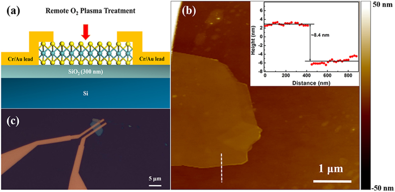
(a) Cross-sectional schematic of a back-gated MoS2 transistor treated with remote O2 plasma. (b) AFM image of a few- layer MoS2 flake on a 300-nm SiO2 substrate. The inset shows the cross-sectional plot along the white line in (b). (c) Optical image of the device using the flake in (b) as the channel. The substrate acts as a back gate. The channel length and width of the device are 1 and 4.2 μm, respectively.
Figure 4. Electrical characterization of the few-layer MoS2 transistor.
(a,b) are the transfer and output characteristics for the original MoS2 transistor. (c,d) are the transfer and output curves for the same device after a 60 s remote O2 plasma treatment. The insets in (a) and (c) show the Ids–Vds curves with back-gate voltages of 5, 15, 25 and 35 V. The linear relationship between the current and voltage within −40 ~ 40 mV indicated that the Cr/Au electrodes form perfect ohmic contacts. All these curves were acquired at room temperature.
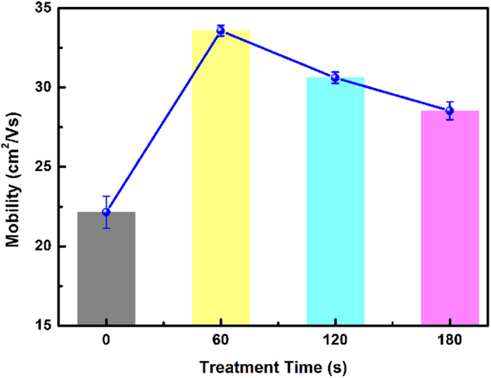
The evolution of the device mobility is tested with different pretreatment time. As shown in Fig. 5, the mobility of the device reaches its peak value with 60 s pretreatment, and decreases slightly with a prolonged pretreatment time, but still higher than the original value. Error bars of Fig. 5 are contributed from repeated measurements each time. To verify the experimental phenomenon, many other back-gate devices were fabricated and tested in the same manner. As expected, a similar phenomenon was observed, proving these results were not a coincidence. This indicates that there is a compromise between the mobility and pretreatment time. It should be noticed that the optimized pretreatment time should be different with different instruments.
Figure 5. Device mobility evolution with the remote O2 plasma pretreatment time.
Discussion
Figure 6 shows the top gate transfer characteristics and leakage current of a few layer MoS2 transistor with top gate dielectric deposited using remote oxygen plasma pretreatment. Top gate dielectric of this device is 60 cycles Al2O3 (about 6.6 nm) which was deposited at 300 °C with 60 s remote oxygen plasma pretreatment. L = 1 μm and W = 5 μm are the channel length and channel width, respectively. For all the measurements in Fig. 6, back gate of the device is grounded as shown in Fig. 6a. From the inset of Fig. 6b, the linear relationship between Ids and Vds within −40 mV −40 mV indicates that Cr/Au electrodes form perfect ohmic contacts with the MoS2 channel. In addition, for all the transfer curves presented in Fig. 6b, great on/off ratio of the current over 108 can be observed within the ±3 V range of the top gate voltage. Top gate leakage current is also measured in the same device. Compared to previously reported top-gate leakage of 2 pA/μm2 within 2 MV/cm1,8, as shown in Fig. 6c, the leakage current is less than 5 × 10⁻¹³ A (about 0.1 pA/μm2) in the measurement range of −3 V to 3 V (4.5 MV/cm). This leakage is much smaller and at same time with an ultrathin gate oxide. The field effect mobility of this top gate device is extracted using Equation (1) discussed above, which was 28 cm2/Vs under Vds = 0.5 V with the SS to be 101 mV/dec.
Figure 6. Top gate characteristics of a few-layer MoS2 transistor.
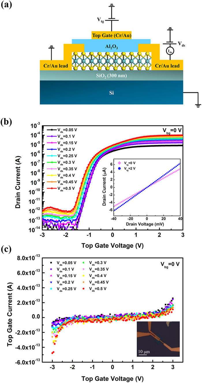
(a) Cross-sectional schematic of the top-gated devices together with the electrical connections. (b) Ids – Vtg curves with Vds ranging from 50 mV to 500 mV. The inset shows the Ids – Vds curves with the top gate voltages of 0 V and 2 V. (c) Top gate leakage current of the device. Optical image of the top gate device is attached as the inset of (c). Top gate dielectric of this device is 60 cycles Al2O3 deposited with 60 s remote oxygen plasma pretreatment. All these measurements were performed at room temperature with the back gate grounded.
In summary, uniform Al2O3 growth on the MoS2 basal plane was successfully achieved by applying a remote O2 plasma pretreatment before ALD, and the mechanism was investigated systematically. After a remote oxygen plasma pretreatment, the oxygen species are physically adsorbed onto the surfaces of the MoS2 flakes and act as nucleation sites for the ALD cycles. The transport studies reveal an extra benefit of this method, which is that unlike many other methods that might sacrifice the device mobility to achieve uniform high-κ growth, this method improves the device mobility by 50%. Furthermore, top-gated MoS2 transistor with ultrathin Al2O3 dielectric was also fabricated. With only 6.6 nm Al2O3 as dielectric, which is the thinnest top gate dielectric ever reported so far, the device shows impressive leakage about 0.1 pA/μm2 at 4.5 MV/cm. Besides, the top-gated device shows great on/off ratio of over 108, subthreshold swing (SS) of 101 mV/dec and a mobility of 28 cm2/Vs. According to the mechanism, it is believed that this method can also be adopted for high-κ growth on other two dimensional nanostructures and used in other devices. With further investigations and optimizations, this method could play an important role in the future nanoelectronics.
Methods
Preparation of the few-layer MoS2 flakes
Ultrathin layers of MoS2 were obtained from bulk crystals (SPI supplies Brand) using the classical tape-based mechanical exfoliation method commonly used for graphene, then transferred onto degenerately doped Si substrates covered with 300 nm SiO2. The thicknesses of these flakes were determined with a Bruker Multimode 8 atomic force microscope (AFM).
Atomic layer deposition of Al2O3 on MoS2 flakes and characterization
Some of the MoS2 flakes were loaded into the Picosun R200 ALD chamber for direct Al2O3 deposition. During the deposition, TMA and H2O served as the aluminum and oxygen precursors, respectively, and different growth temperatures and pulse time were adopted to observe their impacts. For some of the flakes, the remote O2 plasma pretreatments were carried out in the same chamber before Al2O3 was deposited. Here, “remote” means that the plasma source is located remotely from the substrate stage, such that the substrate is not involved in the generation of the plasma. It is then carried to the sample surface by the carrier gas31. The X-ray photoelectron spectroscopy (XPS) system used was made by SPECS GmbH. The X-ray source for data acquisition during the in-situ characterization was SPECS XR50 X-ray source. Considering that the signal intensity was not so strong due to the low density of MoS2 flakes on the substrate and the signal intensity might be further weakened by using an X-ray monochromator, we finally carried out the in-situ characterization using a non-monochromatic XPS source. In the in-situ XPS measurements, all the spectra were taken using a Mg Kα X-ray source (hν = 1253.6 eV). The working pressure in the ultra-high-vacuum (UHV) chamber for the data acquisition was maintained at the magnitude of 10−10 mbar. The element library and the quantification factors used during measurements were provided via the system SpecsLab2 software, and after the measurements, the data analysis was carried out using CasaXPS software. The binding energies in the XPS spectra were calibrated in the conventional way against the adventitious carbon C 1s singlet (Eb = 284.6 eV). The Raman spectra of the MoS2 flakes before the remote O2 plasma treatment were measured with a Renishaw inVia Raman microscope in air using a 514 nm laser. Then after going through the in-situ XPS characterization mentioned above, Raman spectra of the same sample was measured again with all the measurement settings to be the same.
MoS2 transistors fabrication
The degenerately doped Si substrate and the 300-nm SiO2 layer served as the back gate and the gate dielectric, respectively. The source and drain contacts were formed using electron-beam lithography followed by deposition of 10 nm Cr and 70 nm Au. The electrical properties of the transistors were measured with an Agilent B1500 semiconductor device parameter analyzer.
Additional Information
How to cite this article: Yang, W. et al. The Integration of Sub-10 nm Gate Oxide on MoS2 with Ultra Low Leakage and Enhanced Mobility. Sci. Rep. 5, 11921; doi: 10.1038/srep11921 (2015).
Supplementary Material
Acknowledgments
This work was supported by the NSFC (61376092, 51172046), Shanghai Rising-Star Program (13QA1400400, 14QA1400200), Program of Shanghai Subject Chief Scientist (14XD1400900) and the S&T Committee of Shanghai (14521103001).
Footnotes
Author Contributions W.Y. fabricated the samples, analyzed the results and drafted the manuscript. W.Y. and Y.G. performed the measurements. Q.S. and P.Z. contributed to designing this research and analyzing the results. D.Z., L.C. and S.D. supplied valuable discussions about the analysis. All authors reviewed the manuscript.
References
- Radisavljevic B., Radenovic A., Brivio J., Giacometti V. & Kis A. Single-layer MoS2 transistors. Nat. Nanotechnol. 6, 147–150 (2011). [DOI] [PubMed] [Google Scholar]
- Radisavljevic B., Whitwick M. B. & Kis A. Integrated Circuits and Logic Operations Based on Single-Layer MoS2. ACS Nano 5, 9934–9938 (2011). [DOI] [PubMed] [Google Scholar]
- Liu K. et al. Growth of Large-Area and Highly Crystalline MoS2 Thin Layers on Insulating Substrates. Nano Lett. 12, 1538–1544 (2012). [DOI] [PubMed] [Google Scholar]
- Fang H. et al. High-Performance Single Layered WSe2 p-FETs with Chemically Doped Contacts. Nano Lett. 12, 3788–3792 (2012). [DOI] [PubMed] [Google Scholar]
- Sarkar D. et al. MoS2 Field-Effect Transistor for Next-Generation Label-Free Biosensors. ACS Nano 8, 3992–4003 (2014). [DOI] [PubMed] [Google Scholar]
- Yoon Y., Ganapathi K. & Salahuddin S. How Good Can Monolayer MoS2 Transistors be. Nano Lett. 11, 3768–3773 (2011). [DOI] [PubMed] [Google Scholar]
- Late D. J., Liu B., Matte H., Dravid V. P. & Rao C. Hysteresis in Single-Layer MoS2 Field Effect Transistors. ACS Nano 6, 5635–5641 (2012). [DOI] [PubMed] [Google Scholar]
- Liu H. & Ye P. MoS2 Dual-Gate MOSFET with Atomic-Layer-Deposited Al2O3 as Top-Gate Dielectric. IEEE Electron Dev. Lett. 33, 546–548 (2012). [Google Scholar]
- Kim S. et al. High-mobility and low-power thin-film transistors based on multilayer MoS2 crystals. Nat. Commun. 3, 1011 (2012). [DOI] [PubMed] [Google Scholar]
- Bao W., Cai X., Kim D., Sridhara K. & Fuhrer M. S. High mobility ambipolar MoS2 field-effect transistors: Substrate and dielectric effects. Appl. Phys. Lett. 102, 042104 (2013). [Google Scholar]
- Li S. et al. Thickness-Dependent Interfacial Coulomb Scattering in Atomically Thin Field-Effect Transistors. Nano Lett. 13, 3546–3552 (2013). [DOI] [PubMed] [Google Scholar]
- Min S. et al. Nanosheet thickness-modulated MoS2 dielectric property evidenced by field-effect transistor performance. Nanoscale 5, 548–551 (2013). [DOI] [PubMed] [Google Scholar]
- Lee H. S. et al. MoS2 Nanosheet Phototransistors with Thickness-Modulated Optical Energy Gap. Nano Lett. 12, 3695–3700 (2012). [DOI] [PubMed] [Google Scholar]
- Lee H. S. et al. MoS2 Nanosheets for Top-Gate Nonvolatile Memory Transistor Channel. Small 8, 3111–3115 (2012). [DOI] [PubMed] [Google Scholar]
- Fang H. et al. Degenerate n-Doping of Few-Layer Transition Metal Dichalcogenides by Potassium. Nano Lett. 13, 1991–1995 (2013). [DOI] [PubMed] [Google Scholar]
- Pezeshki A. et al. Top and back gate molybdenum disulfide transistors coupled for logic and photo-inverter operation. J. Mater. Chem. C 2, 8023–8028 (2014). [Google Scholar]
- Zou X. et al. Interface Engineering for High-Performance Top-Gated MoS2 Field-Effect Transistors. Adv. Mater. 26, 6255–6261 (2014). [DOI] [PubMed] [Google Scholar]
- Krasnozhon D., Lembke D., Nyffeler C., Leblebici Y. & Kis A. MoS2 Transistors Operating at Gigahertz Frequencies. Nano Lett. 14, 5905–5911 (2014). [DOI] [PubMed] [Google Scholar]
- Liu H., Xu K., Zhang X. J. & Ye P. D. The integration of high-k dielectric on two-dimensional crystals by atomic layer deposition. Appl. Phys. Lett. 100, 152115 (2012). [Google Scholar]
- Liu H. et al. Statistical Study of Deep Submicron Dual-Gated Field-Effect Transistors on Monolayer Chemical Vapor Deposition Molybdenum Disulfide Films. Nano Lett. 13, 2640–2646 (2013). [DOI] [PubMed] [Google Scholar]
- McDonnell S. et al. HfO2 on MoS2 by Atomic Layer Deposition: Adsorption Mechanisms and Thickness Scalability. ACS Nano 7, 10354–10361 (2013). [DOI] [PubMed] [Google Scholar]
- Azcatl A. et al. MoS2 functionalization for ultra-thin atomic layer deposited dielectrics. Appl. Phys. Lett. 104, 111601 (2014). [Google Scholar]
- Shah P. B. et al. Analysis of temperature dependent hysteresis in MoS2 field effect transistors for high frequency applications. Solid-State Electron. 91, 87–90 (2014). [Google Scholar]
- Felten A., Eckmann A., Pireaux J. J., Krupke R. & Casiraghi C. Controlled modification of mono- and bilayer graphene in O2, H2 and CF4 plasmas. Nanotechnology 24, 355705 (2013). [DOI] [PubMed] [Google Scholar]
- Cui N. Y., Brown N. & McKinley A. An AFM study of the topography of natural MoS2 following treatment in an RF-oxygen plasma. Appl. Surf. Sci. 151, 17–28 (1999). [Google Scholar]
- Cui N. Y., Brown N. & McKinley A. An AFM study of a laboratory-grown single-crystal MoS2 surface following radio-frequency oxygen plasma treatment. Appl. Surf. Sci. 158, 104–111 (2000). [Google Scholar]
- Eda G. et al. Photoluminescence from Chemically Exfoliated MoS2. Nano Lett. 11, 5111–5116 (2011). [DOI] [PubMed] [Google Scholar]
- Brown N., Cui N. Y. & McKinley A. An XPS study of the surface modification of natural MoS2 following treatment in an RF-oxygen plasma. Appl. Surf. Sci. 134, 11–21 (1998). [Google Scholar]
- Bertrand P. A. Surface-phonon dispersion of MoS2. Phys. Rev. B 44, 5745–5749 (1991). [DOI] [PubMed] [Google Scholar]
- Windom B. C., Sawyer W. G. & Hahn D. W. A Raman Spectroscopic Study of MoS2 and MoO3: Applications to Tribological Systems. Tribol. Lett. 42, 301–310 (2011). [Google Scholar]
- Profijt H. B., Potts S. E., van de Sanden M. & Kessels W. Plasma-Assisted Atomic Layer Deposition: Basics, Opportunities, and Challenges. J. Vac. Sci. Technol. A 29, 050801 (2011). [Google Scholar]
Associated Data
This section collects any data citations, data availability statements, or supplementary materials included in this article.


