

Abstract
Bioelectronics, electronic technologies that interface with biological systems, are experiencing rapid growth in terms of technology development and applications, especially in neuroscience and neuroprosthetic research. The parallel growth with optogenetics and in vivo multi-photon microscopy has also begun to generate great enthusiasm for simultaneous applications with bioelectronic technologies. However, emerging research showing artefact contaminated data highlight the need for understanding the fundamental physical principles that critically impact experimental results and complicate their interpretation. This review covers four major topics: 1) material dependent properties of the photoelectric effect (conductor, semiconductor, organic, photoelectric work function (band gap)); 2) optic dependent properties of the photoelectric effect (single photon, multiphoton, entangled biphoton, intensity, wavelength, coherence); 3) strategies and limitations for avoiding/minimizing photoelectric effects; and 4) advantages of and applications for light-based bioelectronics (photo-bioelectronics).
1. Introduction to Neurotechnologies
Microelectrodes and optics have independently experienced rapid growth across technological development and emerging applications, especially in neuroscience and neuroprosthetic research. These bioelectronic tools play a critical role in advancing our understanding of basic neuroscience such as behavior, decision-making, memory, plasticity, neural circuitry, connectivity, neurological diseases, and brain injuries 1-4. More recently, these technologies have demonstrated the ability to restore functional motor control in study participants with tetraplegia through a direct brain interface with a robotic arm 5, 6. Multi-modal approaches to discretely perturb and record brain signals at the cellular and molecular level will dramatically advance our understanding of the brain as well as advance treatment and intervention strategies in the clinic.
Electrodes allow direct readouts of the brain through recording of single-unit and multi-unit action potentials, local field potentials, and changes in neurochemical concentrations. In addition, these electrodes provide direct input into the brain by employing electrical stimulation paradigms. Advances in microfabrication and packaging techniques have increased the number or density of recording sites as well as a variety of designs. Advances in biomaterials have further reduced device size, strengthening durability, improving flexibility, increasing electrical properties, attenuating tissue inflammation, and enhancing tissue integration 7-18.
On the other hand, advances in light- or optic-based methods to stimulate and record brain activity have led to a fundamental shift in bioelectronics and neuroscience research:
Optogenetics is one of these tools. This genetic manipulation tool inserts code to manufacture and place light-sensitive proteins in the membrane of neurons that function as ion channels 19. In essence, exposing these cells directly to a specific light frequency excites the light-sensitive protein subunit which in turn causes a conformational change that selectively opens these channels, resulting in the precise control of the activity of these neurons. This genetic manipulation can be targeted to specific cell types such as excitatory and inhibitory neurons allowing for manipulation of neuronal circuits that was not previously possible 20, 21. The optogenetic toolset includes channels that not only target cation fluxes, but also anion fluxes enabling the control of brain activity that promotes or inhibits action potential generation.
Another significant advance for the readout of brain activity has been the development of genetically encoded calcium indicators, laboratory engineered chimeric proteins expressed in neurons that increase fluorescence with the influx of calcium that accompanies neuronal firing of action potentials 22. These techniques have been combined with multiphoton microscopy to enable in vivo imaging at subcellular resolution deep in the tissue (>500-900 μm) 23. Continued work with genetically encoded fluorescent proteins and promoters has expanded the cell types and subcellular components that can be studied in vivo 24.
Researchers were initially enthusiastic to combine these electronic- and optic- input and output modalities. However, the emerging data reveal new challenges and boundaries, some beset by Heisenberg's ‘observer principle’. For example, optical excitation generates photoelectric artefacts that interfere with electronics. On the other hand, understanding the mechanisms underlying this artefact can lead to new opportunities in technology design, experimental techniques, and applications for optics based implantable devices in clinical and basic research applications.
2. Basic Principles Governing the Photoelectric Effect
The photoelectric effect is the generation of voltage or current in a material upon exposure to light energy, first observed by Alexandre Edmond Becquerel on a photovoltaic cell in 1839 25. He observed that unequal illumination of two identical electrodes placed in an electrolyte generated electrochemical currents. Therefore, photoelectric effect generated from a photovoltaic cell is called the Becquerel Effect. In 1887, Heinrich Hertz reported the production and reception of electromagnetic waves in the presence of high frequency light 26. Albert Einstein in 1905 further described these effects for which he was awarded the Nobel Prize 27. One important characteristic of the photoelectric effect is that electrons are only dislodged by the photoelectric effect if light reaches or exceeds a threshold frequency, below which no electrons can be emitted from the electric conductor regardless of the amplitude and temporal length of exposure of light. This is described by the equation(s):
| (1) |
| (2) |
where E is the energy of the absorbed photon, v is frequency of the light, h is Plank's constant, c is the speed of light, λ is the wavelength of the light, and ψ is the photoelectric work function. Additionally, v0 and λ0 are the light frequency and wavelength threshold necessary to generate photocurrents, respectively. The photoelectric effect is observed when E > ψ for single photon events. (Note that it is possible to change the wavelength of the light without changing its frequency, for example by passing it through another material, which in turn will not alter the photoelectric properties. However, for most biomedical applications and neural technologies, wavelength and frequency can be equated through Eq. 1 & 2.) Further, the generated current is proportional to:
| (3) |
where j is current and Φ is photon flux, which is proportional to intensity divided by the area of the material:
| (4) |
3. Light Penetration in Tissue
Incoherent light sources emit photons over narrow or broad wavelengths with randomly oriented phase. Although incoherent light sources can be collimated into beams, their efficiency is not high and generally require a greater surface area to capture the same intensity (e.g. number of photons) (Fig. 1a, Eq. 4). On the other hand, coherent light sources or lasers (light amplification by stimulated emission of radiation) polarize photons at virtually a single frequency into a narrow beam. Because photons emitted from lasers have correlated phase, they are diffraction-limited and maintain a narrow beam over relatively large distance (Fig. 1b).
Figure 1.
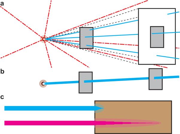
Light Sources. (a) With incoherent light sources at greater distances, a greater surface area is needed to capture the same number of photons. (b) Coherent light sources are diffraction-limited and maintain a narrow beam. (c) Blue light (top) scatters more quickly and has s hallower penetration compared to near infrared light (bottom).
While coherence from lasers is maintained in ideal media, biological tissue is highly turbid. As light penetrates through turbid media, photons undergo absorption and scatter which limits the penetration of light in thick samples (>100-200μm), especially high energy, high frequency photons (Fig. 1c). The penetration of light into tissue is empirically described by the Beer-Lambert Law, which is a function of the medium's optical scattering coefficient (μS’) and the absorption coefficient (μA). While the scattering coefficient in brain tissue decreases with increasing wavelength, the absorption coefficient has a more complex profile. At UV and visible wavelengths (200-550 nm), both optical absorption and scattering are high and light is highly attenuated. In the so-called “near-IR window” between 550-900 nm, the optical absorption coefficient is low enough (μA~0.05 mm-1) to allow light to “diffuse” through several centimetres of tissue. Above 900 nm, water absorption dominates the signal and light is heavily attenuated. Thus, the limited penetration depth of visible light (excitation 400-600 nm) is a major concern, especially when considering the high visible light absorption (400-600 nm) of blood cells (haemoglobin) through the neurovasculature and also in the presence of blood brain barrier (BBB) disruption and leakage if the devices are implanted into the brain 9, 18, 23, 24, 28.
4. Material Dependent Properties
The photoelectric effect is only observed when the threshold frequency is exceeded, that is, photons at the threshold wavelength or lower have sufficient energy to excite the electron. This cut-off threshold is determined by the properties of the device material.
4.1 Orbital Theory and Band Theory
In atoms and molecules, electrons occupy orbitals of discrete energy levels characterized by the atomic or molecular orbital theory (Fig. 2a) 29. Each atomic orbital is identified by a unique set of values and three quantum numbers: n (1, 2, 3, 4...), l (s, p ,d, f...), and m (1, 3, 5, 7...). These describe the electron's energy, angular momentum, and magnetic quantum number when occupying that orbital. Electrons reside in these orbitals following the Pauli Exclusion Principle, which states that they possess half-integer spins and cannot occupy the same quantum state of an orbital simultaneously. In the ground state, electrons fill the lowest available orbitals (Fig. 2a). In molecular orbital theory, linear combination of atomic orbitals represents bonds between atoms.
Figure 2.

Simplified representation of relative electron energy levels. (a) Relative orbital electron energy levels as represented by Atomic Orbital Theory (e.g. C). (b) Relative orbital electron energy levels as represented by Band Theory. (c) Dopants alter the Photoelectric Work Function (ψ) for pdopants (left) and n-dopants (center). Dopant level can also alter the wok function (ψ > ψ′) and shift the rate of photoelectric excitation in a material (right).
Band theory describes that each of these orbitals of a solid material occupy a band of energy range (Fig. 2b). Energy bands or allowed bands represent energy ranges that an electron may occupy. Band gaps or forbidden bands are energy states that electrons cannot occupy. The valence band describes the highest occupied energy band when electrons pack the lowest available energy states (Fig. 2a-b). Above the valence band is the conduction band. When the electron reaches the conduction band, it allows the electron to dissociate from its atom or molecule and become a free charge carrier.
These band structures help illustrate many properties in solid-state physics, including electrical conductivity and optical absorption. In metallic conductors, the valence band and conduction band overlap, making it very easy to conduct electricity. Semiconductors are materials in which the band gap is small such that a small amount of heat or light can delocalize valence electrons into the conduction band. Insulators are materials with very large band gaps between the valence band and conduction band. For photoactivation to occur, electrons in the valence band must be excited by photons with enough energy to reach the conduction band.
4.2 Dopants
Doping agents are trace impurities that are inserted into a substance at low concentrations to alter the electrical or optical properties of a material (Fig. 2c). P-type dopants have fewer valence electrons than the substrate material. E.g. boron, which has 3 valence electrons, is a popular p-dopant for increasing the conductivity of carbon and silicon substrates which have 4 valence electrons. As a result, p-type dopants are positively charged carriers and are good electron acceptors. The p-dopants accept excited electrons from the valence band of the substrate material into a lower conduction band of the dopant. This reduces the photoelectric work function necessary for photoactivation (ψp < ψ0: Fig. 2c).
In contrast, n-type dopants have more valence electrons making them negatively charged carriers and good electron donors. E.g. nitrogen or phosphate has 5 valence electrons to silicon's 4. Therefore, electrons excited from the higher energy valence bands of the n-dopants flow into the conduction band of the bulk material. As a result, the n-dopant reduces the photoelectric work function (ψn < ψ0: Fig. 2c). Lastly, the amount of dopants in a material impacts its rate of photoelectric events and can also decrease the threshold for photoactivation (ψn’ < ψn < ψ0: Fig. 2c). In practice, the level of doping impacts the sensitivity of the material to the photoelectric effect.
4.3 Types of Photoactivation
When photons collide with electrons, it transfers some energy into the electron. Eventually that absorbed energy is released. The release of that energy can take one of several closely related but mechanistically different modes depending on the material: 1) photoconductive; 2) photoelectrochemical; 3) photovoltaic; 4) photothermal; and 5) fluorescence (light activated electromagnetic radiation) (Fig. 3). While different applications may ideally have a preferred photoexcitation mode, most devices in practice simultaneously photoactivate multiple modes, sometimes leading to interchanged usage of these terms.
Figure 3.
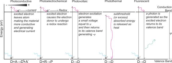
Modes of Photoactivation. A high energy photon (blue) excites an electron into the conduction band generating ψ, and then generates a current (photoconductive), a redox reaction (photoelectrochemical), - ψ voltage (photovoltaic), heat (magenta: photothermal), or a photon (green: fluorescence or light activated electromagnetic radiation). D represents the atom or molecule from which the electron is excited and A represents an electron acceptor. R and P represent a reactant and product of a redox reaction, respectively. (R and P may represent multiple chemical species and charges.)
Photoconductive mode is when a material becomes more electrically conductive from the absorption of light. Here, photon-excited electrons are separated from their holes (the atom or molecule) associated with it. The electron is then separated from its electron hole by an applied electric field bias resulting in the electron flowing towards the cathode. This can be easily observed in diodes or with dopants where the valence band the electron originally belonged to and the conduction band that it is excited into belong to different atoms. With metallic conductors, the generated current is proportional to the intensity of light and the available surface area of the material.
Photoelectrochemical mode separates an electron from its hole. In photoelectrochemical activation, the high energy electron initiates a redox reaction at an electrode/electrolyte interface30. As a result, corrosion of the photoactivated material may occur, altering the electrical properties of the interface. In Becquerel's closed circuit photoelectric cells, the illuminated metal releases electrons into the electrolyte. The electron holes created by the galvanic action are filled from the un-illuminated metal, which in turn collects electrons from the solute.
Photovoltaic mode occurs in a purely solid-state device when an electron's energy level is excited by a photon without an electric field bias, but the electron is not separated from its hole restricting photocurrent out of the device. In contrast to photoelectrochemical activation, photovoltaic activation does not lead to a chemical reaction30. This means that Faradaic charge transfer does not occur. The movement of the electron from one energy state to another generates a small voltage. While the ψ voltage from individual electrons may be undetectable from the thermal noise in in vivo recording experiments, the cumulative intensity and surface area dependent photovoltaic effect can generate large electrical artefacts during electrophysiology recording. This large voltage, low power artefacts are sometimes called anomalous photovoltaic effects or bulk photovoltaic effects and caused by grains or domains adding in series, or by non-centrosymmetry in crystals. This cumulative voltage change can lead to a transient non-Faradaic charge transfer at the electrode-electrolyte interface when the light source is turned on or turned off. During continuous illumination with the same intensity light, the rate of electrons rising to the conduction band and falling to the valence band reaches equilibrium, and no net non-Faradaic charge transfer is observed.
Photothermal mode generally occurs when a photon transfers energy into an electron, but the absorbed energy is not translated into the generation of another photon, electron release, or increase in the energy state of the electron. Instead, the absorbed energy or excess energy is released as kinetic energy or heat. It is also worth noting that the electrical conductivity (σ) of isotropic conductors is related to thermal conductivity (k) as described by the Wiedemann-Franz Law:
| (6) |
where L is the Lorenz number and T is temperature.
The Rutherford model of atoms explains that most of matter is empty space 31, photons can penetrate multiple atomic layers of a material before exciting an electron or experiencing coherent scattering (i.e. Thomson scattering). With metallic conductors, the heat can be transferred to adjacent atoms and passed down the length of the material. However, because insulators do not conduct thermal energy as readily, most of the generated heat does not transfer into the tissue at biologically relevant light intensities.
Furthermore, in photoelectromagentic mode, absorbed energy in the excited electron is released as a fluorescent photon (i.e. a lower energy photon and therefore of higher wavelength than the incident photon). Some biological tissues have fluorescent properties, termed autofluorescence. Although rare, autofluorescence may generate an artefact in imaging studies. Lastly, while photomagnetic effects exist32, the level of optic power necessary to generate any detrimental artefact precludes concern for in vivo experiments with current technologies 33.
5. Optics Dependent Properties
With incoherent light source, electrons are only dislodged by the photoelectric effect if light reaches or exceeds a threshold frequency, regardless of the amplitude and temporal length of exposure of light. However, these threshold frequency and wavelengths described by Einstein only apply to single-photon events. Nobel laureate Maria Goppert-Mayer described in 1931 that multi-photon events, where two or more photons simultaneously collide at the target, can greatly reduce the cutoff threshold 34. In multi-photon photoelectric activation, E does not scale linearly with N. Instead EN can be described as:
| (7) |
where N is the number of simultaneously colliding photons and S is some positive scalar value 35. Beyond multi-photon events, Einstein, Podolsky, and Rosen hypothesized an additional two-particle entangled state 36. These were further described and characterized as:
| (8) |
where f(I) is a function of light intensity and Bv is a material based coefficient. This experimentally derived expression represents additional quantum level photon-photon or photon-electron-photon interactions 37, 38. For example, in high intensity light, a second photon can collide with an electron within the excitation lifetime following the first collision, especially with coherent laser sources 39. In addition, even in a single photon beam, two single-photons can “entangle” through quantum level photon-photon interactions to from a single biphoton ‘packet’ 37, 38 (See Ref 40 for Review).
The unexpected observation is that for N-photon events, longer wavelengths can be used to generate the photoelectric effect and meet its energy criterion than would be predicted by multiplying the threshold wavelength by N. This entanglement, in part, explains why photoelectric artefacts can be observed during optogenetic stimulation experiments with blue light (e.g. 473 nm) despite many electrode materials having threshold <<473 nm (or band gaps >>2.63 eV). Furthermore, laser power injection into the tissue decreases with increases in wavelength. This means that more photoelectric events can be generated with longer wavelength while remaining within tissue heating safety limits. Current research, particularly in the telecommunications field are focused on improving the yield of entangling pairs of photons into biphotons 39.
6. Strategies and Limitations to Avoid or Attenuate the Photoelectric Effect
The growth of optogenetics and in vivo multi-photon microscopy has generated great enthusiasm for simultaneous applications with bioelectronic technologies. However, artefact contaminated data highlight the need for understanding how these artefacts impact experimental results and complicate their interpretation (Fig. 4). In particular photoelectric artefact from laser pulses can generate electrical artefact that appears similar to a single-unit action potential waveform. Several strategies have been used to attenuate the photoelectric effect during optical imaging experiments, such as two-photon microscopy, but each approach has specific limitations. Depending on the experiment and the specific type of data needed for the study, certain strategies may not sufficiently attenuate the photoelectric artefacts.
Figure 4.

Photoelectric Artefact Contaminated Electrophysiological Data. (a) Photoelectric artefact recorded in brain from a tungsten electrode (1MΩ) placed 200 μm deep in cortex during photo-stimulation delivered using an optic fiber placed in the pial surface coupled to a 473 nm laser source (1mW delivered at the fiber tip). The trace in (a) was obtained by aligning all photostimulation events and extracting the three largest principal components. These consistent features can be minimized or eliminated from electrophysiological traces by removing these components from a PCA decomposition or by linear regression. (b) This raw trace shows photoelectric artifact with photo-stimulation onset and offset. (c) Artefact was minimized by linear regression of the trace in (a). Traditional spike detection analysis can be used to assess the actual spiking activity. ††
6.1 Optical and Analytical Approach
One method often discussed in confocal and two-photon microscopy studies is to zero or blank the laser light amplitude as it is rastering over the electrode location. While this attenuates the photoelectric effect, it does not eliminate it. In section 3, photon scattering was discussed. Because photons scatter in tissue, some of the light can scatter back and trigger the photoelectric effect below the mask.
Another approach is to use incoherent light. This reduces the Becquerel effect, since at relatively far distances, the light illuminates all electrodes and substrates with equal intensities. The attenuation is best when all electrode sites, conductive electrical trace, and references are implanted at the same depth, in the same way, and with the same surface area exposed to the light source. However, using a reference electrode identical to the recording electrode can contribute to a substantial increase in the electrical noise floor, especially with single-unit recording electrodes that generally have high-impedance electrode sites. Even with a larger reference electrode, often necessary for single-unit recordings, common-average referencing (CAR) of multiple identical (and identically illuminated) electrodes can dramatically attenuate the Becquerel effect 41. However, controlling equal and simultaneous photon collision of all electrodes/traces and references is much more difficult. While CAR can attenuate some of the artefact, it is unable to completely eliminate it. CAR requires a large number of recording sites (>10) and to remove Becquerel effect they must be the same size and placed very closely together such that the tissue scattered light equally illuminates the recording sites, but are far enough apart that electrical crosstalk is minimized. This becomes especially difficult for rastered images using a laser.
Using a substantially longer wavelength than the photoelectric cut-off threshold can reduce photoelectric excitation. Even with multi-photon activation, longer wavelengths increase the N requirement in Eq. (7) and (8) for sufficient photoexcitation to exceed the cut-off threshold. In addition to better tissue depth penetration, this was a motivator for the development of longer wavelength activated opsins for optogenetics 42, 43. However, when combining fluorescent detection in the visible light range with coherent light sources, the light intensities necessary to detect fluorescence will generally generate overwhelming photoelectric artefacts. This is typically true because the percent yield of detected fluorescent photons over generated fluorescent photons is much lower than the number of photoelectric events detected on the electrode. Fluorescent photons are generally emitted in random directions, and photon scattering, photon absorption, and the sensitivity of the detector lead to low fluorescent detection. On the other hand, all photoelectric events on an electrode contribute to the detected electrical artefact.
Moving light sources away from the electrode also attenuates photoelectric activation. For incoherent light sources, moving the light source away from the electrode decreases the number of photons per second that collide with the electrode. The effectively reduced intensity at the electrode leads to attenuation of the photoelectric effect. For coherent light sources, focusing the beam away from the electrode similarly attenuates the number of scattered photons and entangled photons that reach the electrode surface. However, this can impact neuroscience studies, since it prevents electrophysiological studies of neural action potential at the centre of the light beam.
For the study of local field potentials, high frequency pulses can be used with a low pass filter. The low pass filter removes high frequency signals such as those generated by an optical pulse with a short pulse width. The LFP response can then be analysed after the end of the pulse train. However, this can filter out any spike information, and the artefact can still accumulate charge on the electrode (especially depending on the electrode type and material) with extended high frequency pulse trains. A principal component analysis (PCA) strategy can be used to isolate the majority of repetitive artefact patterns that introduce large amounts of variance into the data stream44; however, additional strategies are necessary to characterise the variability of photoelectric artefacts in order to completely remove them from electrophysiological data. High-pass filtering has been proposed as an artefact mitigation strategy for neural spike data, especially for long light pulses. Unfortunately, prolonged continuous excitation leads to neurotoxic excitation and/or denaturation of the channels leading to neuronal death.
One approach used for the analysis of neural activity following optical stimulation is to analyse the change in the firing rate of single-unit and multi-unit activity after the end of the optic pulse. A problematic trade-off is to detect neural spike activity within the optical pulse duration, since the spikes will be buried in the artefact. Unlike evoking activity in sensory systems, there is effectively no latency for optogenetic activation. It is therefore likely that recorded spikes will be generated from the first downstream neurons activated through synaptic transmission by the neuron depolarized from opsin excitation. This would require the pulse width to be shorter than the synaptic latency. In turn, lower numbers of photons will be emitted in an ultra-short pulse, and therefore, the probability of a photon exciting the opsin ion channel-gating subunit is also lowered. The challenge then becomes generating sufficient opsin activation to reliably generate action potentials within a small time window of a single pulse within laser safety power constraints, especially at the tissue depth of interest assuming the opsin allows for reliable channel function (opening and closing) in this time frame.
A preferred approach to mitigate optical artefacts from electrophysiological recordings is to exploit the temporal consistency of the artefacts (Fig. 4). A common approach involves identifying consistent sources of variance in the recordings that can be removed by means such as principal component analysis. Artefact-related components can be removed by zeroing these entries and the data recomposed or, alternatively, these components can be removed from the data by linear regression. An example of the latter is shown in Figure 4c. It is necessary to inspect these components since they often include highly synchronized spiking activity. If the artefact and evoked spiking activity cannot be easily separated, measurements of the artefact alone outside the brain can be used as an alternative. The computation time and demands of these and other approaches can vary tremendously and often determine the choice of approach. Another typical problem in these recordings is that the artefact saturates the amplifier which further complicates the artefact removal process and should be avoided if possible.
6.2 Materials Based Approach
One approach often discussed is the use of transparent electrode materials. Insulators have very large bandgaps compared to conductors and semiconductors. In insulators, even when sufficient excitation occurs, nearby atoms in the lattice are unable to conduct the excited electron. The material dependent challenge is in finding biomaterials that are sufficiently conductive but possess bandgaps that are wide enough to not absorb photons at the relevant wavelengths (accounting for multi-photons and biphotons). Dopants are often necessary to make the materials electrically conductive. Transparent conductors such as tin-doped indium-oxide (indium tin oxide), poly(3,4-ethylenedioxythiophene) (PEDOT: doped with a counter ion), or graphene, have bandgaps at wavelengths shorter than 380 nm and have been often proposed as solutions for photoelctronic applications. Indium tin oxide films are mostly transparent (~80%) at visible wavelength. However, for in vivo applications and with infrared light, indium tin oxide oxidizes over time, resulting in darkening of the film, increasing electrical impedance, and impacting biocompatibility properties45. Furthermore, additional challenges described below have thwarted demonstration of these materials effectively eliminating the photoelectric artefact.
In addition, these materials must be deposited as a thin-film on a substrate. Conductive polymers, like PEDOT, are also typically grown on conductive substrates. Naturally if a conductive substrate is used, any photon transmitted through the transparent conductive film can still activate the photoelectric effect on the underlying electrode material.
It is also important to note that these transparent conductive films are not completely transparent. The Rutherford model highlights that atoms are mostly empty space. However, these transparent conductive films still possess electrons that can be excited by photons, especially with coherent light sources. The fact that these transparent conductive films become opaque or darker at larger thicknesses confirms the idea that these films are not fully transparent. This has led to the motivation of using ultrathin mostly transparent materials in electrodes. Recently, one to four layer graphene sheets were developed with ~90% optical transparencies 46. However, even these devices generated significant photoelectric artefact with optical stimulation for channelrhodopsin-2 in vivo 46. In in vitro cell culture or ex vivo slice culture, the light source power can be significantly reduce such that the artefact is diminished to negligible levels 47. This is because the light scattering distance in culture is substantially reduced for slices (0-20 μm), while in vivo greater distances are required to reach beyond Layer I to where neural cell bodies reside. In these conductive films, the photoelectric excitations are in series, accumulating into a large electrical artefact.
The opposite approach to using transparent films is to employ an optic block coating. This optic block absorbs or scatters the photons prior to reaching the electrode material. However, the Rutherford model again highlights that the optic block may need to be relatively thick, adding substantial amount of volume to the electrode before it is able to block 100% of the light. Furthermore, the electrode recording site still needs to be exposed to the tissue which can provide a window for direct or tissue scattered light to produce photoelectric effects.
Photon scattering materials may locally increase the fluorescence for imaging and photon absorbing materials may lead to tissue heating, though the level of impact has yet to be characterized. Along these lines, coaxial cable or double-shielded coaxial style electrodes have also been proposed. While the external shielding may protect the bulk internal wire from the photoelectric effect, the design needs to be carefully considered to prevent the Becquerel effect resulting from a differential in photoexcitation between the different conductive layers. This design also leads to greater probe volume and does not eliminate the photoelectric effect at the recording electrode site.
While reducing the electrode size does not eliminate the photoelectric effect, it can attenuate it. Equation (4) shows that decreasing the surface area can decrease the number of direct and tissue scattered photons that photoexcite electrons on the electrode. Advancements in microfabrication have led to ultrasmall electrical traces and recording sites, but due to strength and durability constraints, they are often made on a backbone substrate. A particularly common electrode substrate in microfabrication is boron-doped silicon, which is used for its chemical etch-stop property. However, heavy boron-doping of silicon (p-doped) leads to enhanced conductivity and reduced photoelectric bandgap of the substrate. With microfabricated silicon arrays where the polycrystalline silicon electrical traces and doped silicon substrates are separated by a thin insulating silicon oxide film, this can also lead to additional capacitive charging related electrical artefacts.
The most effective approach to date for eliminating the photoelectric artefact is to replace the solid-state electrical conductor with an ionic electrical conductor. Ionic conduction occurs through the movement of charged ions through the liquid instead of electrons flowing through the conduction band of a solid. Therefore, the photoelectric artefact remains negligible. These ionic conductor devices are typically made from glass pipettes that are heated and pulled to a sharp tip. A 3-20 μm recording opening is made at the tip, and the pipette is filled with saline or artificial cerebral spinal fluid. A solid conductor, usually a short Pt or Ag/AgCl wire, is inserted into the back of the pipette to connect to the recording system. With a long pipette, the wire end of the pipette can be placed relatively far away from the coherent light such that the number of photons that impact the wire is negligible.
While this method has been used to effectively avoid the photoelectric effect, it does have several limitations. Pulled glass pipettes have very narrow thicknesses near the tip. A very thin dielectric film can lead to the formation of a simple low-pass RC circuit. However, this can be addressed by using a negative capacitor amplifier often employed in commercial patch clamp systems. Less addressable challenges are limitations in microelectrode array design availabilities. Currently, there are no microfabricated ionic conductor electrode arrays with very controlled site spacing and geometries. More importantly, the most significant challenge with ionic conductor electrodes is the limitations for chronic applications. The pulled glass is very thin and brittle. Furthermore, glial cells can infiltrate into the fluidic channel and effectively clog it.
While many strategies have been proposed or used to attenuate the photoelectric effect, each approach has specific limitations. It is important to consider these limitations on the specific data collected for the study during experimental design.
7. Applications for photoelectric and photothermal technology
Neuroscience studies involving light for imaging (e.g. confocal or two-photon microscopy) or stimulation (e.g. optogenetics) often require eliminating or minimizing light artefacts in the images or photoelectric artefacts from the neurological data collected to enable a meaningful interpretation of the results. However, the photoelectric artefact challenge also presents a technological opportunity. New bioelectric devices can be engineered to leverage the photoelectric or phototermal effects to address existing challenges and explore new applications.
7.1 Classical Challenges with Neural Stimulation
7.1.1 Electrical Stimulation
Numerous challenges currently exist with electrical neurostimulation that impact the performance efficacy over time. One challenge with electrical stimulation is the tradeoff between safety limits and spatial selectivity of the stimulated neural population 48. Stimulation electrodes with small surface areas can result in high charge densities that lead to permanent damage of the electrode or permanent damage to the tissue and nearby neurons 8, 48, 49. Therefore, large stimulation electrodes are frequently used, which leads to a spatially broad orthodromic and antidromic activation of neurons50, 51.
Related to the size of the electrodes is the size of the implanted device. Ultra-small sub-cellularsized devices produce less mechanical strain on the surrounding tissue following implantation 28. They also maintain improved electrical characteristics by eliciting less glial scarring, which can form an ionic barrier around electrodes thereby reducing its efficacy over time. Neurons in these glial scar areas also undergo apoptosis, increasing the distance to the nearest neurons and in turn, further decreasing efficacy over time. Chronically implanted ultra-small electrodes additionally improved electrical coupling to nearby neurons by maintaining proximity to neurons. 12, 52.
Furthermore, electrical stimulation implants are currently tethered, for example to the skull. This increases the probability of infection or traumatic impact-induced mechanical failure, or even positional drift 4, 7, 53. Rigid tethering also increases the impact of mechanical mismatch induced strain that aggravates reactive tissue reaction, glial scarring, and neuronal loss. 54. As a result, electrical stimulation loses its effectiveness to excite neural tissue over time. Furthermore, inflammation and encapsulation is minimized when a free-floating device is fully implanted into the brain compared to when part of the device is penetrating out of the brain surface 55. In addition, mechanical strain can result in positional drifts and movement of the electrode which may be detrimental for probing fine changes in neural circuits longitudinally (eg. plasticity).
These studies have led to the hypothesis that flexible devices reduce strain on the surrounding tissue, and thereby reduce glial scarring and neural degeneration around implants 56. However, there are currently no materials that have the necessary compliance to match the brain tissue, possess the necessary electrical properties and mechanical strength required to develop ultrasmall electrodes 7, 18. While electrical stimulation is the oldest technique to stimulate neurons, multiple technological limitations exist in the advancement of this method.
7.1.2 Optogenetic Stimulation
Optogenetics relies on the insertion of light-sensitive ion channels to activate neurons. This is one approach to eliminate the tethering requirement. One of the strengths of optogenetics is that it offers a genetic selectivity of specific cell types through the use of genetic promoters. However, one constraint for optogenetics is the requirement for genetic manipulation. Often, optogenetic mouse lines express opsins in specific cell types, but over a large spatial area. Alternatively, viral manipulation improves spatial expression selectivity, but large variability from surgery as well as unpredictability, and a lack of control over virus diffusion, transduction rate, and light scatter, make it difficult to precisely reproduce expression. As a result, optogenetic models often lead to poor control over genetically similar but functionally different neurons (e.g. neurons with different tuning directions).
As an example, two adjacent pyramidal neurons in Layer V of motor cortex may express the same exact phenotype. However, on a systems level, they maybe functionally connected to different networks. For example, one of these phenotypically identical neurons may increase firing rate during rightward movement, while the other increases firing rate during leftward movement. Lack of control over precise targeting individual neurons makes activating the same discrete population of neurons longitudinally very difficult. Addressing issues resulting from highly scattering biological tissue and/or poor control over virus diffusion radius and virus transduction rate present non-negligible engineering challenges. Furthermore, the long-term risks of viral manipulation have not been comprehensively characterized.
7.1.3 Infrared Stimulation
An emerging alternative is to use IR light to wirelessly stimulate peripheral neural tissue 57. IR neural stimulation may have better spatial selectivity than electrical stimulation; however, the penetration depth is limited due to light absorption and hence higher laser power requirements. IR neural stimulation in the brain provides an additional number of challenges due to poor mechanistic understanding and dramatic anatomical differences between brain and peripheral nerves 58-60. Empirical evidence suggests IR neural stimulation works well around 900 nm wavelength, just outside the ‘near IR window’, where optical absorption of water molecules is relatively high 58, 61, 62. Current understanding of IR neural stimulation is that it creates a thermal gradient that facilitates the opening of heat sensitive ion channels 63, 64. The efficacy of this stimulation mode may also be improved by employing transgenic manipulation to introduce or increase the expression of these heat sensitive ion channels. Because of the high energy absorption required for neural stimulation, IR stimulation has limited penetration depth (300-600 μm) and stimulation frequency (<4 Hz) due to concerns for permanent thermally induced tissue heating injury 58, 61, 62. This in turn, limits use in applications that require high frequency stimulation such as deep brain stimulation and evoking sound perception.
7.1.4 Radio-Frequency and Ultrasonic Stimulation
While alternatives exist using “antennas” to convert RF or ultrasonic energy into electrical current, their chronic biocompatibility in vivo require further evaluation and development 65-67. Further, these stimulation modes are unable to selectively stimulate individual channels in multi-implant “arrays” since near-field RF excitation is difficult to focus below several centimeters resolution. Lastly, the transducers necessary for ultrasound and RF stimulation can be relatively large and heavy. Particularly in the case of ultrasound, pulses cannot be coupled over relatively long distances unlike with optic fibres or electric wires.
7.1.5 Electromagnetic Stimulation
Transcranial magnetic stimulation allows for non-invasive excitation or inhibition of large areas of the brain 68. However, this technique cannot target neurons at a cellular resolution and requires very large induction coils. In contrast, magneto-thermal stimulation locally heats tissue similarly to infrared neural stimulation 69. Electromagnetic oscillations are used to thermally excite ferromagnetic particles. By altering the particle size and property, different nanoparticles can be selectively excited with different oscillation frequencies. While, electromagnetic oscillations have improved tissue heating safety and depth penetration, the large electromagnetic coils needed currently preclude it from being a wearable device. Similarly to ultrasound, the oscillations cannot be coupled over relatively long distances unlike with optic fibers or electric wires. Furthermore, additional research is also necessary to identify its efficacy in vivo for repeated long-term neural stimulation.
7.2 New Technology Opportunities
The ‘near-IR window’ (550-900 nm), where the combination between optical scattering and optical absorption of biological tissue is the lowest, presents several opportunities for photoelectric and photothermal applications (Fig. 5).
Figure 5.
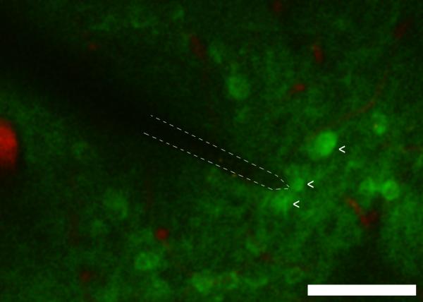
Free floating carbon-fiber electrode photostimulated with 900 nm wavelength laser at 150Hz and 10 mW excited GCaMP3 neurons in mouse brain in vivo at a 300 μm depth. Bright green cells indicate neurons (arrow) that greatly increased firing rate with photostimulation. Red labels vasculature. Scale bar = 100 μm. †
7.2.1 Photoelectric Neural Stimulation and Wireless Controlled-Release Drug Delivery
The photoelectric artefact can be used for free-floating electrical stimulation. This eliminates the tethering related material failure and inflammation induced tissue injury. Interestingly, metallic conductors naturally generate a negative voltage pulse (Fig. 6). This is advantageous since a cathodic (negative) electrical pulse more readily evokes action potentials compared to equal but opposite anodic (positive) electric pulse. The discrepancy in neurons is due to the direction of the electrochemical gradient and orientation of the subunit controlling the gating mechanisms of voltage-gated sodium channels.
Figure 6.
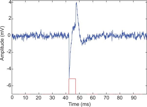
Photoelectric Artifact with a 473 nm laser set to 10mW. Red indicates 5 ms wide laser pulse onto a photosensitive 10 Ω-cm boron-doped silicon substrate. Ionic currents (blue) were recorded 100 μm away in 0.5% agarose in PBS. Note: the lead electrical artifact is negative and a positive deflection occurs after the laser pulse ends. †††
The electrical current generated by the photoelectric effect can also be further enhanced by employing photoelectric cells 70. These cells are composed of p-n or p-i-n diodes that further facilitates the transfer of excited electrons as electrical current to enhance the generated voltage 70-78. (p-n diode is made from adjoining p-doped and n-doped semiconductor. p-i-n diode has a lightly doped intrinsic semiconductor layer separating the p-doped and n-doped layer.) However, in order to deliver a sufficient electrical pulse to depolarize neurons, these photoelectric cells need to be relatively large implants.
Studies have also shown that the optical scattering property of biological tissue is advantageous in this regard, since it allows tolerance for small displacements due to in vivo micromotion 70. In addition, optic band pass filters can also be employed to enable multiplexing of multichannel photoelectric stimulation 79. This is not only important for depth-wise selectivity in 3D multichannel arrays, but also lateral selectivity as optical scattering can lead to activation of devices 400-1,000 μm away.
It is worth noting that the most efficient photodiode materials (e.g., cadmium telluride, gallium arsenide) used in solar cell technologies are incredibly toxic to the tissue. While non-toxic alternatives (doped carbon or crystalline silicon) are also being researched, their conversion efficiencies may need to be improved for specific applications. For small silicon devices, it is worth recognizing that it may also be ideal for transient applications as they have been shown to dissolve at a rate of 2-4.5 nm/day 80.
While silicon is a popular material for microfabrication with good biocompatibility with tissue, coating n-doped silicon with SWNTs has demonstrated enhanced power conversion efficiency by >60% 81, 82. Carbon can come in multiple forms with a variety of electrical properties: 1) single-walled CNTs (SWNT); 2) double-walled CNTs (DWNT); 3) multi-walled CNTs (MWNT); 4) Graphene; 5) Graphene oxide, 6) carbon fiber; 7) diamond; etc. Therefore, carbon possess a wide range of direct bandgaps depending on its form, (m,n) index orientations and dopants. [For (n,m); CNTs are metallic (n = m), quasi-metallic (n-m = 3X, where X is an integer), semiconducting (others)]. CNTs possess strong photoabsorption from IR to ultraviolet wavelengths, high power conversion efficiency, very high non-Faradaic charge transfer, very low Faradaic charge transfer, high carrier mobility, and reduced carrier transport scattering 72, 83, 84. Specifically, carbon has nearly an order of magnitude higher capacitive charge transfer capacity, as well as over 8 orders of magnitude greater resistance than traditional metals, indicating minimized Faradaic charge transfer – which could otherwise damage the tissue or electrode material 84. This makes carbon an ideal photovoltaic material85 as well as a great electrical stimulation electrode material 84, 86-91. Furthermore, carbon and CNTs also have tunable photovoltaic properties and electric properties through the incorporation of dopants 71-74, 76-78, 92-95. Lastly, SWNTs have been shown to form ideal p-n junction photovoltaic diodes that reach the theoretical limits 85, 96.
A combination of materials and optics advancement may enable long lasting, ultra-small devices that can activate a localized spatial area over millimetres and centimetres of tissue depth. There is a strong desire for the ability to activate a discrete population of neurons in a brain region or axons in a large nerve bundle. In the brain, the ability to repeatedly activate the same discrete population of neurons over time allows the ability to map plastic changes in the neural network and connectivity from memory and learning paradigms. Advances in two-photon microscopy and genetically encoded calcium indicators enable the ability to visualization changes in the structure of axons, dendrites, and dendritic spines of the discretely probed neurons over time. The neural stimulation of peripheral nerves are also of growing interest because they are less invasive targets compared to the central nervous system. Neuromodulation from stimulating peripheral nerves is being pursued for a variety of conditions including rheumatoid arthritis, cardiac hypertension, pain, wound healing, obesity, neurological diseases, and mental health.
Lastly, recent advances in conductive polymers have focused on controlled-release drug delivery. Mesoporous silica nanoparticles, carbon nanotubes, and graphene have been employed as reservoir substrates from drug loading 97-102. The drug loaded reservoirs are then incorporated into the conductive polymer during electrochemical deposition. Electrical stimulation can then be used to expel the drug from the reservoir and locally deliver pharmaceutical treatments. Here, the photovoltaic properties of the conductive polymers and carbon reservoir substrates may be exploited for wireless drug delivery.
7.2.2 Photothermal Neural Stimulation and Photothermal Tumor Ablation Therapy
An emerging alternative to photoelectric neural stimulation is photothermal neural stimulation. Infrared and near-infrared neural stimulation work best within wavelength ranges where the water's optical absorption coefficient peaks. However, this in turn indicates that light penetration becomes very limited. In order to address this issues, many researchers have turned to plasmonic nanoparticles with wavelengths within the ‘near-IR window’ (550-900 nm).
Plasmonic nanoparticles are particles that can couple with photons with wavelengths that are far larger than the particle due to the dielectric-particle interface and therefore, exhibit unique scattering and absorbance properties 103. Like ferromagnetic nanoparticles, the shape and aspect ratio of nanorods allow tuning to specific ranges of wavelengths 104. This is particularly important as nanoparticles that have lengths much greater than 2,000 nm exhibit significant reactive tissue responses 105. The ultimate goal with these nanoparticles is to be able to bypass invasive surgery and deliver them to the target neurons through minimally invasive injections or ingestion and delivery to their target cells using special coatings that exploit the host's natural transport system.
Using wavelengths from the ‘near-IR window’ allows for deeper light penetration. Gold plamonic nanorods then act as photon scavengers that convert light into localized thermal energy 106. The thermal gradient transiently changes the membrane capacitance and can activate temperature-sensitive ion channels 63, 64. Early results have demonstrated the viability acutely in vivo to enhance photothermal near-IR neural stimulation 107. Interestingly, when the gold nanorods were bound to the surface of the neuron membrane in vitro using amine-terminated polyethylene glycol, photothermal excitation of the nanorods led to neural inhibition 108. This inhibition was temporary and could be reversed when the light source was turned off.
Of course, applications of plasmonic nanoparticles are not limited to neural stimulation. Gold nanorods at higher stimulation levels can lead to tissue ablation 109, 110. This is particularly useful for the suppression and ablation of tumor cells 111. However, these plasmonic gold nanorods undergo photothermal reshaping at relatively low work functions (0.6-1.5 eV). This reshaping is driven by curvature-induced surface diffusion at temperatures well below the melting point threshold 112. For chronic applications, the stability of nanorods and nanoparticles for stable operation and prolonged biocompatibility need to be considered, even at body temperature which is well below the melting point of these particles.
7.3 New Methodology Opportunities
Electrical stimulation has multiple variables that can be studied: pulse shape/waveform; pulse width; symmetric or asymmetric charge balancing waveform; inter-pulse interval width; pulse amplitudes (voltage or current); stimulation frequency; pulse train duration; and pulse train frequency. While the Rheobase curve demonstrates that shorter pulse-widths require exponentially greater stimulation strengths 113, there are multiple factors that can influence the accuracy of these prediction, especially at lower pulse-widths 114. At very high stimulation frequencies and amplitudes, electroporation and thermal injuries lead to cell death, which may have applications in cancer therapy, but precludes neural stimulation 115, 116. However, ultrafast electrical stimulation has yet to be comprehensively explored. The cost of developing a system capable of subnanosecond electrical stimulation is substantial. However, using ultrafast coherent lasers and photoelectrically activated electrodes may allow electrochemical biophysics studies of subcellular structures and membranes in new ways, although additional research is necessary 117.
Conclusions
Recent advances in implantable neural microelectrodes and neural optical techniques have enabled studying the nervous system in more intimate ways. However, the optical and material dependent photoelectric principles highlight new challenges in combining electrical technology and optical techniques. While eliminating these artefacts that contaminate neural data is difficult, there is promise in leveraging the photoelectric and photothermal effects for next generation bioelectric devices. Additional research remains necessary for understanding and improving the reliability and longevity as well as further developing systems-level device design for practical research and clinical prosthetic application. Nevertheless, optical bioelectric technologies will allow researchers to interface with the body in new ways.
Supplementary Material
Acknowledgements
Financially support was provided by NIH R01 (5R01NS062019) and NIH K01 (K01NS066131). The authors would like to thank Drs. J Luc Peterson (Lawrence Livermore National Laboratories) and Eli Van Cleve (Tribogenics, Inc.) for useful discussions.
Biography
 Takashi D.Y. Kozai is currently a Research Assistant Professor in the Department of Bioengineering at the University of Pittsburgh. He received a B.A. Magna Cum Laude with Distinction in Molecular, Cellular, and Developmental Biology, and another B.A. with Distinction in Biochemistry from the University of Colorado, Boulder in 2005. He earned his M.S. (2007) and PhD (2011) degree in Biomedical Engineering from the University of Michigan, Ann Arbor. His primary interests include the areas of elucidating molecular and cellular pathways of brain injuries and diseases, in vivo two-photon imaging, neural engineering, implantable medical devices, biomaterials, and neurotechnologies.
 Alberto Vazquez is currently a Research Assistant Professor in the Departments of Radiology and Bionengineering at the University of Pittsburgh. He currently works on neuronal, metabolic and vascular brain imaging approaches in health and disease. He obtained his BS in Biomedical Engineering from Rensselear Polytechnique Institute in Troy, NY, his M.S. in Bioengineering from the University of Pittsburgh and his Ph.D. in Biomedical Engineering from the University of Michigan.
Footnotes
B6;CBA-Tg(Thy1-GCaMP3) mice (Jackson Laboratory, Bar Harbor, ME were prepared using previously established methods 28. All experimental protocols were approved by the University of Pittsburgh, Division of Laboratory Animal Resources and Institutional Animal Care and Use Committee. In vivo GCaMP3 mice imaging was conducted using a microscope consisting of a scan head (Praire Technologies, Madison, Wi) and a Ti:sapphire laser (Mai Tai DS; Spectra-Physics, Menlo Park, Ca) at 900 nm calibrated to 10 mW power. Free-floating carbon-fiber Microthread electrode was used for photostimulation.
B6.Cg-Tg(Thy1-COP4/EYFP)9Gfng/J mice (Jackson Laboratory, Bar Harbor, ME) were prepared using previously described methods 3. All experimental protocols were approved by the University of Pittsburgh Institutional Animal Care and Use Committee. Electrophysiological recordings were obtained using a tungsten electrode (WPI Inc, Sarasota, FL) and a Plexon system (MAP, Plexon Inc., Dallas, TX). The light or photo-stimulus recording data was reused from Ref 3. Custom PCA and linear regression routines were implemented in MATLAB (Mathworks, Natick, MA).
Blue light photo-stimulus was delivered using a power-adjustable, transistor-transistor logic (TTL)-controlled, 473 nm laser diode unit (CystalLaser, Ince, Reno, NV, USA) connected to the optic fiber with a core diameter of 125 μm (S-405-HP, ThorLabs, Inc., Newton, NJ, USA) as previously described 3. Photosensitive heavily boron-doped silicon substrates were custom ordered from NeuroNexus Technologies (Ann Arbor, Mi). Recording electrodes were custom pulled glass pipettes filled with ACSF and Pt or Ag/AgCl wire or a carbon fiber electrode (Carbostar-1 with a tip diameter of 5 µm and 1 MΩ Impedance, Kation Scientific, Minneapolis, MN, USA). Electrical recording was conducted using an RX7 recording system with a Medusa Preamplifier (Tucker-David Technologies, Alachua FL) and synchronized to the laser using TTL. 0.5% agarose phatom was prepared as previously described 13.
References
- 1.Guitchounts G, Markowitz JE, Liberti WA, Gardner TJ. J Neural Eng. 2013;10:046016. doi: 10.1088/1741-2560/10/4/046016. [DOI] [PMC free article] [PubMed] [Google Scholar]
- 2.Vazquez AL, Murphy MC, Kim S-G. Brain connectivity. 2014;4:727–740. doi: 10.1089/brain.2014.0276. [DOI] [PMC free article] [PubMed] [Google Scholar]
- 3.Vazquez AL, Fukuda M, Crowley JC, Kim S-G. Cerebral Cortex. 2014;24:2908–2919. doi: 10.1093/cercor/bht147. [DOI] [PMC free article] [PubMed] [Google Scholar]
- 4.Kozai TDY, Du Z, Gugel ZV, Smith MA, Chase SM, Bodily LM, Caparosa EM, Friedlander RM, Cui XT. Journal of Neuroscience Methods. 2015;242:15–40. doi: 10.1016/j.jneumeth.2014.12.010. [DOI] [PMC free article] [PubMed] [Google Scholar]
- 5.Collinger JL, Wodlinger B, Downey JE, Wang W, Tyler-Kabara EC, Weber DJ, McMorland AJ, Velliste M, Boninger ML, Schwartz AB. Lancet. 2012;381(9866):557–564. doi: 10.1016/S0140-6736(12)61816-9. [DOI] [PMC free article] [PubMed] [Google Scholar]
- 6.Simeral JD, Kim SP, Black MJ, Donoghue JP, Hochberg LR. J Neural Eng. 2011;8:025027. doi: 10.1088/1741-2560/8/2/025027. [DOI] [PMC free article] [PubMed] [Google Scholar]
- 7.Kozai TDY, Catt K, Li X, Gugel ZV, Olafsson VT, Vazquez AL, Cui XT. Biomaterials. 2015;37:25–39. doi: 10.1016/j.biomaterials.2014.10.040. [DOI] [PMC free article] [PubMed] [Google Scholar]
- 8.Kozai T, Alba N, Zhang H, Kotov N, Gaunt R, Cui X. In: Nanotechnology and neuroscience: nano-electronic, photonic and mechanical neuronal interfacing. Vittorio MD, Martiradonna L, Assad J, editors. Springer; New York, New York, NY: 2014. pp. 71–134. DOI: 10.1007/978-1-4899-8038-0, ch. Chapter 4: Nanostructured Coatings for Improved Charge Delivery to Neurons. [Google Scholar]
- 9.Kozai TDY, Gugel Z, Li X, Gilgunn PJ, Khilwani R, Ozdoganlar OB, Fedder GK, Weber DJ, Cui XT. Biomaterials. 2014;35:9255–9268. doi: 10.1016/j.biomaterials.2014.07.039. [DOI] [PubMed] [Google Scholar]
- 10.Kolarcik CL, Catt K, Rost E, Albercht IN, Bourbeau D, Du Z, Kozai TDY, Luo X, Weber DJ, Cui XT. Journal of Neural Engineering. 2015;12:016008. doi: 10.1088/1741-2560/12/1/016008. [DOI] [PMC free article] [PubMed] [Google Scholar]
- 11.Gilgunn, R. PJK, Kozai TDY, Weber DJ, Cui XT, Erdos G, Ozdoganlar OB, Fedder GK. Micro Electro Mechanical Systems (MEMS). 2012 IEEE 25th International Conference on.2012. pp. 56–59. [Google Scholar]
- 12.Kozai TDY, Langhals NB, Patel PR, Deng X, Zhang H, Smith KL, Lahann J, Kotov NA, Kipke DR. Nature materials. 2012;11:1065–1073. doi: 10.1038/nmat3468. [DOI] [PMC free article] [PubMed] [Google Scholar]
- 13.Kozai TDY, Kipke DR. J Neurosci Methods. 2009;184:199–205. doi: 10.1016/j.jneumeth.2009.08.002. [DOI] [PMC free article] [PubMed] [Google Scholar]
- 14.Zhang H, Patel PR, Xie Z, Swanson SD, Wang X, Kotov NA. ACS Nano. 2013;7:7619–7629. doi: 10.1021/nn402074y. [DOI] [PubMed] [Google Scholar]
- 15.Ware T, Simon D, Liu C, Musa T, Vasudevan S, Sloan A, Keefer EW, Rennaker RL, 2nd, Voit W. J Biomed Mater Res B Appl Biomater. 2014;102:1–11. doi: 10.1002/jbmb.32946. [DOI] [PubMed] [Google Scholar]
- 16.Harris JP, Hess AE, Rowan SJ, Weder C, Zorman CA, Tyler DJ, Capadona JR. J Neural Eng. 2011;8:046010. doi: 10.1088/1741-2560/8/4/046010. [DOI] [PMC free article] [PubMed] [Google Scholar]
- 17.Azemi E, Lagenaur CF, Cui XT. Biomaterials. 2011;32:681–692. doi: 10.1016/j.biomaterials.2010.09.033. [DOI] [PMC free article] [PubMed] [Google Scholar]
- 18.Kozai TDY, Jaquins-Gerstl A, Vazquez AL, Michael AC, Cui XT. ACS Chemical Neuroscience. 2015;6:48–67. doi: 10.1021/cn500256e. [DOI] [PMC free article] [PubMed] [Google Scholar]
- 19.Boyden ES, Zhang F, Bamberg E, Nagel G, Deisseroth K. Nature neuroscience. 2005;8:1263–1268. doi: 10.1038/nn1525. [DOI] [PubMed] [Google Scholar]
- 20.Alivisatos AP, Andrews AM, Boyden ES, Chun M, Church GM, Deisseroth K, Donoghue JP, Fraser SE, Lippincott-Schwartz J, Looger LL. ACS Nano. 2013;7:1850–1866. doi: 10.1021/nn4012847. [DOI] [PMC free article] [PubMed] [Google Scholar]
- 21.Klapoetke NC, Murata Y, Kim SS, Pulver SR, Birdsey-Benson A, Cho YK, Morimoto TK, Chuong AS, Carpenter EJ, Tian Z. Nature methods. 2014;11:338–346. doi: 10.1038/nmeth.2836. [DOI] [PMC free article] [PubMed] [Google Scholar]
- 22.Chen T-W, Wardill TJ, Sun Y, Pulver SR, Renninger SL, Baohan A, Schreiter ER, Kerr RA, Orger MB, Jayaraman V, Looger LL, Svoboda K, Kim DS. Nature. 2013;499:295–300. doi: 10.1038/nature12354. [DOI] [PMC free article] [PubMed] [Google Scholar]
- 23.Kozai TDY, Marzullo TC, Hooi F, Langhals NB, Majewska AK, Brown EB, Kipke DR. J Neural Eng. 2010;7:046011. doi: 10.1088/1741-2560/7/4/046011. [DOI] [PMC free article] [PubMed] [Google Scholar]
- 24.Kozai TDY, Vazquez AL, Weaver CL, Kim SG, Cui XT. J Neural Eng. 2012;9:066001. doi: 10.1088/1741-2560/9/6/066001. [DOI] [PMC free article] [PubMed] [Google Scholar]
- 25.Becquerel A-E. Comptes Rendus. 1839;9:1839. [Google Scholar]
- 26.Hertz H. Annalen der Physik. 1887;267:983–1000. [Google Scholar]
- 27.Einstein A. Annalen der Physik. 1905;322:132–148. [Google Scholar]
- 28.Kozai TDY, Li X, Bodily LM, Caparosa EM, Zenonos GA, Carlisle DL, Friedlander RM, Cui XT. Biomaterials. 2014;35:9620–9634. doi: 10.1016/j.biomaterials.2014.08.006. [DOI] [PMC free article] [PubMed] [Google Scholar]
- 29.Cotton FA, Wilkinson G, Gaus PL, Bryant R. Basic inorganic chemistry. Wiley; New York: 1995. [Google Scholar]
- 30.Archer MD. Physica E: Low-dimensional Systems and Nanostructures. 2002;14:61–64. [Google Scholar]
- 31.Rutherford E. The London, Edinburgh, and Dublin Philosophical Magazine and Journal of Science. 1911;21:669–688. [Google Scholar]
- 32.Oliveira SL, Rand SC. Physical Review Letters. 2007;98:093901. doi: 10.1103/PhysRevLett.98.093901. [DOI] [PubMed] [Google Scholar]
- 33.Fisher WM, Rand SC. Journal of Applied Physics. 2011;109:064903. [Google Scholar]
- 34.Göppert-Mayer M. Annalen der Physik. 1931;401:273–294. [Google Scholar]
- 35.Krasnoholovets V. Indian Journal of Theoretical Physics. 2001;49:1–32. [Google Scholar]
- 36.Einstein A, Podolsky B, Rosen N. Physical Review. 1935;47:777. [Google Scholar]
- 37.Panarella E. In: Quantum Uncertainties. Honig W, Kraft D, Panarella E, editors. Vol. 162. Springer; US: 1987. pp. 237–269. ch. 13. [Google Scholar]
- 38.Panarella E. Found Phys. 1974;4:227–259. [Google Scholar]
- 39.Ward MB, Dean MC, Stevenson RM, Bennett AJ, Ellis DJP, Cooper K, Farrer I, Nicoll CA, Ritchie DA, Shields AJ. Nat Commun. 2014;5:3316. doi: 10.1038/ncomms4316. [DOI] [PubMed] [Google Scholar]
- 40.Shih Y. Reports on Progress in Physics. 2003;66:1009. [Google Scholar]
- 41.Ludwig KA, Miriani RM, Langhals NB, Joseph MD, Anderson DJ, Kipke DR. J Neurophysiol. 2009;101:1679–1689. doi: 10.1152/jn.90989.2008. [DOI] [PMC free article] [PubMed] [Google Scholar]
- 42.Klapoetke NC, Murata Y, Kim SS, Pulver SR, Birdsey-Benson A, Cho YK, Morimoto TK, Chuong AS, Carpenter EJ, Tian Z, Wang J, Xie Y, Yan Z, Zhang Y, Chow BY, Surek B, Melkonian M, Jayaraman V, Constantine-Paton M, Wong GK-S, Boyden ES. Nat Meth. 2014;11:338–346. doi: 10.1038/nmeth.2836. [DOI] [PMC free article] [PubMed] [Google Scholar]
- 43.Chuong AS, Miri ML, Busskamp V, Matthews GAC, Acker LC, Sorensen AT, Young A, Klapoetke NC, Henninger MA, Kodandaramaiah SB, Ogawa M, Ramanlal SB, Bandler RC, Allen BD, Forest CR, Chow BY, Han X, Lin Y, Tye KM, Roska B, Cardin JA, Boyden ES. Nat Neurosci. 2014;17:1123–1129. doi: 10.1038/nn.3752. [DOI] [PMC free article] [PubMed] [Google Scholar]
- 44.Sun L, Hinrichs H. Hum Brain Mapp. 2009;30:3361–3377. doi: 10.1002/hbm.20758. [DOI] [PMC free article] [PubMed] [Google Scholar]
- 45.Pappas TC, Wickramanyake WMS, Jan E, Motamedi M, Brodwick M, Kotov NA. Nano Letters. 2007;7:513–519. doi: 10.1021/nl062513v. [DOI] [PubMed] [Google Scholar]
- 46.Park D-W, Schendel AA, Mikael S, Brodnick SK, Richner TJ, Ness JP, Hayat MR, Atry F, Frye ST, Pashaie R. Nat Commun. 2014;5:5258. doi: 10.1038/ncomms6258. [DOI] [PMC free article] [PubMed] [Google Scholar]
- 47.Kuzum D, Takano H, Shim E, Reed JC, Juul H, Richardson AG, de Vries J, Bink H, Dichter MA, Lucas TH, Coulter DA, Cubukcu E, Litt B. Nat Commun. 2014;5:5259. doi: 10.1038/ncomms6259. [DOI] [PMC free article] [PubMed] [Google Scholar]
- 48.Merrill DR, Bikson M, Jefferys JG. Journal of Neuroscience Methods. 2005;141:171–198. doi: 10.1016/j.jneumeth.2004.10.020. [DOI] [PubMed] [Google Scholar]
- 49.Cogan SF. Annual Review of Biomedical Engineering. 2008;10:275–309. doi: 10.1146/annurev.bioeng.10.061807.160518. [DOI] [PubMed] [Google Scholar]
- 50.Wei XF, Grill WM. Front Neuroeng. 2009;2:15. doi: 10.3389/neuro.16.015.2009. [DOI] [PMC free article] [PubMed] [Google Scholar]
- 51.Han J, Han J, Lee BS, Lim J, Kim SM, Kim H, Kang S. J. Micromech. Microeng. 2012;22:065004. [Google Scholar]
- 52.Seymour JP, Kipke DR. Biomaterials. 2007;28:3594–3607. doi: 10.1016/j.biomaterials.2007.03.024. [DOI] [PubMed] [Google Scholar]
- 53.Barrese JC, Rao N, Paroo K, Triebwasser C, Vargas-Irwin C, Franquemont L, Donoghue JP. Journal of Neural Engineering. 2013;10:066014. doi: 10.1088/1741-2560/10/6/066014. [DOI] [PMC free article] [PubMed] [Google Scholar]
- 54.Biran R, Martin DC, Tresco PA. J Biomed Mater Res A. 2007;82:169–178. doi: 10.1002/jbm.a.31138. [DOI] [PubMed] [Google Scholar]
- 55.Markwardt NT, Stokol J, Rennaker Ii RL. Journal of Neuroscience Methods. 2013;214:119–125. doi: 10.1016/j.jneumeth.2013.01.020. [DOI] [PMC free article] [PubMed] [Google Scholar]
- 56.Subbaroyan J, Martin DC, Kipke DR. J Neural Eng. 2005;2:103–113. doi: 10.1088/1741-2560/2/4/006. [DOI] [PubMed] [Google Scholar]
- 57.Wells J, Kao C, Jansen ED, Konrad P, Mahadevan-Jansen A. J Biomed Opt. 2005;10:064003. doi: 10.1117/1.2121772. [DOI] [PubMed] [Google Scholar]
- 58.Wells J, Kao C, Konrad P, Milner T, Kim J, Mahadevan-Jansen A, Jansen ED. Biophysical. 2007;93:2567–2580. doi: 10.1529/biophysj.107.104786. [DOI] [PMC free article] [PubMed] [Google Scholar]
- 59.Mahadevan-Jansen A, Cayce JM, Friedman R, Roe AW, Konrad PE, Hillman E, Jansen E. 4th International IEEE/EMBS Conference on; 2010; 2010. pp. 3379–3381. DOI: 10.1109/IEMBS.2010.5627920. [DOI] [PMC free article] [PubMed] [Google Scholar]
- 60.Thompson AC, Fallon JB, Wise AK, Wade SA, Shepherd RK, Stoddart PR. Hear. Res. 2015;324:46–53. doi: 10.1016/j.heares.2015.03.005. [DOI] [PubMed] [Google Scholar]
- 61.Richter CP, Matic AI, Wells JD, Jansen ED, Walsh JT., Jr. Laser Photon Rev. 2011;5:68–80. doi: 10.1002/lpor.200900044. [DOI] [PMC free article] [PubMed] [Google Scholar]
- 62.Wells J, Konrad P, Kao C, Jansen ED, Mahadevan-Jansen A. Journal of Neuroscience Methods. 2007;163:326–337. doi: 10.1016/j.jneumeth.2007.03.016. [DOI] [PMC free article] [PubMed] [Google Scholar]
- 63.Shapiro MG, Homma K, Villarreal S, Richter C-P, Bezanilla F. Nat Commun. 2012;3:736. doi: 10.1038/ncomms1742. [DOI] [PMC free article] [PubMed] [Google Scholar]
- 64.Albert ES, Bec J, Desmadryl G, Chekroud K, Travo C, Gaboyard S, Bardin F, Marc I, Dumas M, Lenaers G. Journal of Neurophysiology. 2012;107:3227–3234. doi: 10.1152/jn.00424.2011. [DOI] [PubMed] [Google Scholar]
- 65.Ciofani G, Danti S, D'Alessandro D, Ricotti L, Moscato S, Bertoni G, Falqui A, Berrettini S, Petrini M, Mattoli V, Menciassi A. ACS Nano. 2010;4:6267–6277. doi: 10.1021/nn101985a. [DOI] [PubMed] [Google Scholar]
- 66.Larson PJ, Towe BC. Neural Engineering (NER); 5th International IEEE/EMBS Conference on; 2011; 2011. pp. 265–268. [Google Scholar]
- 67.Harrison RR, Watkins PT, Kier RJ, Lovejoy RO, Black DJ, Greger B, Solzbacher F. Solid-State Circuits, IEEE Journal of. 2007;42:123–133. [Google Scholar]
- 68.Hallett M. Nature. 2000;406:147–150. doi: 10.1038/35018000. [DOI] [PubMed] [Google Scholar]
- 69.Christiansen MG, Senko AW, Chen R, Romero G, Anikeeva P. Applied Physics Letters. 2014;104:213103. [Google Scholar]
- 70.Abdo A, Sahin M, Freedman DS, Cevik E, Spuhler PS, Unlu MS. Journal of Neural Engineering. 2011;8:056012. doi: 10.1088/1741-2560/8/5/056012. [DOI] [PMC free article] [PubMed] [Google Scholar]
- 71.Yang L, Wang S, Zeng Q, Zhang Z, Peng LM. Small. 2013;9:1225–1236. doi: 10.1002/smll.201203151. [DOI] [PubMed] [Google Scholar]
- 72.Cataldo S, Salice P, Menna E, Pignataro B. Energy & Environmental Science. 2012;5:5919–5940. [Google Scholar]
- 73.Camilli L, Scarselli M, Gobbo SD, Castrucci P, Gautron E, De Crescenzi M. Beilstein J Nanotechnol. 2012;3:360–367. doi: 10.3762/bjnano.3.42. [DOI] [PMC free article] [PubMed] [Google Scholar]
- 74.Kim DH, Park JG. Nanotechnology. 2012;23:325401. doi: 10.1088/0957-4484/23/32/325401. [DOI] [PubMed] [Google Scholar]
- 75.Yang L, Wang S, Zeng Q, Zhang Z, Li Y, Zhou W, Liu J, Peng LM. ACS Appl Mater Interfaces. 2012;4:1154–1157. doi: 10.1021/am201778x. [DOI] [PubMed] [Google Scholar]
- 76.Bourdo SE, Saini V, Piron J, Al-Brahim I, Boyer C, Rioux J, Bairi V, Biris AS, Viswanathan T. ACS Appl Mater Interfaces. 2012;4:363–368. doi: 10.1021/am201426y. [DOI] [PubMed] [Google Scholar]
- 77.Castrucci P, Del Gobbo S, Camilli L, Scarselli M, Casciardi S, Tombolini F, Convertino A, Fortunato G, De Crescenzi M. J Nanosci Nanotechnol. 2011;11:9202–9207. doi: 10.1166/jnn.2011.4284. [DOI] [PubMed] [Google Scholar]
- 78.Sadhu V, Nismy NA, Adikaari AA, Henley SJ, Shkunov M, Silva SR. Nanotechnology. 2011;22:265607. doi: 10.1088/0957-4484/22/26/265607. [DOI] [PubMed] [Google Scholar]
- 79.Seymour EÇ, Freedman DS, Gökkavas M, Özbay E, Sahin M, Ünlü MS. Front Neuroeng. 2014;7:00005. doi: 10.3389/fneng.2014.00005. [DOI] [PMC free article] [PubMed] [Google Scholar]
- 80.Hwang S-W, Tao H, Kim D-H, Cheng H, Song J-K, Rill E, Brenckle MA, Panilaitis B, Won SM, Kim Y-S, Song YM, Yu KJ, Ameen A, Li R, Su Y, Yang M, Kaplan DL, Zakin MR, Slepian MJ, Huang Y, Omenetto FG, Rogers JA. Science. 2012;337:1640–1644. doi: 10.1126/science.1226325. [DOI] [PMC free article] [PubMed] [Google Scholar]
- 81.Li Z, Kunets VP, Saini V, Xu Y, Dervishi E, Salamo GJ, Biris AR, Biris AS. Applied Physics Letters. 2008;93:243117. [Google Scholar]
- 82.Jia Y, Cao A, Bai X, Li Z, Zhang L, Guo N, Wei J, Wang K, Zhu H, Wu D, Ajayan PM. Nano Letters. 2011;11:1901–1905. doi: 10.1021/nl2002632. [DOI] [PubMed] [Google Scholar]
- 83.Landi BJ, Raffaelle RP, Castro SL, Bailey SG. Progress in Photovoltaics: Research and Applications. 2005;13:165–172. [Google Scholar]
- 84.Cannizzaro C, Tandon N, Figallo E, Park H, Gerecht S, Radisic M, Elvassore N, Vunjak-Novakovic G. In: Tissue Engineering. Hauser H, Fussenegger M, editors. Vol. 140. Humana Press; 2007. pp. 291–307. ch. 16. [DOI] [PubMed] [Google Scholar]
- 85.Lee JU. Applied Physics Letters. 2005;87:153107. [Google Scholar]
- 86.Luo X, Weaver CL, Zhou DD, Greenberg R, Cui XT. Biomaterials. 2011;32:5551–5557. doi: 10.1016/j.biomaterials.2011.04.051. [DOI] [PMC free article] [PubMed] [Google Scholar]
- 87.de Asis ED, Jr., Nguyen-Vu TD, Arumugam PU, Chen H, Cassell AM, Andrews RJ, Yang CY, Li J. Biomed Microdevices. 2009;11:801–808. doi: 10.1007/s10544-009-9295-7. [DOI] [PMC free article] [PubMed] [Google Scholar]
- 88.Wang K, Fishman HA, Dai H, Harris JS. Nano letters. 2006;6:2043–2048. doi: 10.1021/nl061241t. [DOI] [PubMed] [Google Scholar]
- 89.Jan E, Hendricks JL, Husaini V, Richardson-Burns SM, Sereno A, Martin DC, Kotov NA. Nano Lett. 2009;9:4012–4018. doi: 10.1021/nl902187z. [DOI] [PubMed] [Google Scholar]
- 90.Jiang LQ, Gao L. J Am Ceram Soc. 2006;89:156–161. [Google Scholar]
- 91.Liopo AV, Stewart MP, Hudson J, Tour JM, Pappas TC. J Nanosci Nanotechno. 2006;6:1365–1374. doi: 10.1166/jnn.2006.155. [DOI] [PubMed] [Google Scholar]
- 92.Li C, Xia J, Wang Q, Chen J, Lei W, Zhang X. ACS Appl Mater Interfaces. 2013;5:7400–7404. doi: 10.1021/am401725x. [DOI] [PubMed] [Google Scholar]
- 93.Hamilton CE, Flood DJ, Barron AR. Phys Chem Chem Phys. 2013;15:3930–3938. doi: 10.1039/c3cp50435b. [DOI] [PubMed] [Google Scholar]
- 94.Shim JS, Ahn CH. Biosens Bioelectron. 2012;34:208–214. doi: 10.1016/j.bios.2012.02.004. [DOI] [PubMed] [Google Scholar]
- 95.Hadjinicolaou AE, Leung RT, Garrett DJ, Ganesan K, Fox K, Nayagam DA, Shivdasani MN, Meffin H, Ibbotson MR, Prawer S. Biomaterials. 2012;33:5812–5820. doi: 10.1016/j.biomaterials.2012.04.063. [DOI] [PubMed] [Google Scholar]
- 96.Jung Y, Li X, Rajan NK, Taylor AD, Reed MA. Nano Letters. 2012;13:95–99. doi: 10.1021/nl3035652. [DOI] [PubMed] [Google Scholar]
- 97.Cho Y, Shi R, Ivanisevic A, Ben Borgens R. Nanotechnology. 2009;20:275102. doi: 10.1088/0957-4484/20/27/275102. [DOI] [PubMed] [Google Scholar]
- 98.Freedman MS, Cui XT. Physical Chemistry Communications. 2014;1:15–25. [Google Scholar]
- 99.Weaver CL, LaRosa JM, Luo X, Cui XT. ACS Nano. 2014;8:1834–1843. doi: 10.1021/nn406223e. [DOI] [PMC free article] [PubMed] [Google Scholar]
- 100.Jiang S, Sun Y, Cui X, Huang X, He Y, Ji S, Shi W, Ge D. Synthetic Metals. 2013;163:19–23. [Google Scholar]
- 101.Luo X, Matranga C, Tan S, Alba N, Cui XT. Biomaterials. 2011;32:6316–6323. doi: 10.1016/j.biomaterials.2011.05.020. [DOI] [PMC free article] [PubMed] [Google Scholar]
- 102.Luo X, Cui XT. Electrochem commun. 2009;11:1956–1959. doi: 10.1016/j.elecom.2009.08.027. [DOI] [PMC free article] [PubMed] [Google Scholar]
- 103.Eustis S, El-Sayed MA. Chem Soc Rev. 2006;35:209–217. doi: 10.1039/b514191e. [DOI] [PubMed] [Google Scholar]
- 104.Yong J, Needham K, Brown WG, Nayagam BA, McArthur SL, Yu A, Stoddart PR. Adv. Healthcare Mater. 2014;3:1862–1868. doi: 10.1002/adhm.201400027. [DOI] [PubMed] [Google Scholar]
- 105.Gallentoft L, Pettersson LM, Danielsen N, Schouenborg J, Prinz CN, Linsmeier CE. Biomaterials. 2015;42:172–183. doi: 10.1016/j.biomaterials.2014.11.051. [DOI] [PubMed] [Google Scholar]
- 106.Paviolo C, Thompson AC, Yong J, Brown WG, Stoddart PR. Journal of Neural Engineering. 2014;11:065002. doi: 10.1088/1741-2560/11/6/065002. [DOI] [PubMed] [Google Scholar]
- 107.Eom K, Kim J, Choi JM, Kang T, Chang JW, Byun KM, Jun SB, Kim SJ. Small. 2014;10:3853–3857. doi: 10.1002/smll.201400599. [DOI] [PubMed] [Google Scholar]
- 108.Yoo S, Hong S, Choi Y, Park J-H, Nam Y. ACS Nano. 2014;8:8040–8049. doi: 10.1021/nn5020775. [DOI] [PubMed] [Google Scholar]
- 109.Choi WI, Kim J-Y, Kang C, Byeon CC, Kim YH, Tae G. ACS Nano. 2011;5:1995–2003. doi: 10.1021/nn103047r. [DOI] [PubMed] [Google Scholar]
- 110.Vankayala R, Huang YK, Kalluru P, Chiang CS, Hwang KC. Small. 2014;10:1612–1622. doi: 10.1002/smll.201302719. [DOI] [PubMed] [Google Scholar]
- 111.Popp MK, Oubou I, Shepherd C, Nager Z, Anderson C, Pagliaro L. Journal of Nanomaterials. 2014;2014:450670. [Google Scholar]
- 112.Taylor AB, Siddiquee AM, Chon JW. ACS Nano. 2014;8:12071–12079. doi: 10.1021/nn5055283. [DOI] [PubMed] [Google Scholar]
- 113.Lapicque L. J. Physiol. Pathol. Gen. 1907;9:620–635. [Google Scholar]
- 114.Geddes LA. Biomedical Engineering, IEEE Transactions on. 2004;51:176–181. doi: 10.1109/TBME.2003.820340. [DOI] [PubMed] [Google Scholar]
- 115.Camp JT, Jing Y, Zhuang J, Kolb JF, Beebe SJ, Song J, Joshi RP, Xiao S, Schoenbach KH. Plasma Science, IEEE Transactions on. 2012;40:2334–2347. [Google Scholar]
- 116.Xiao S, Guo S, Nesin V, Heller R, Schoenbach KH. Biomedical Engineering, IEEE Transactions on. 2011;58:1239–1245. doi: 10.1109/TBME.2011.2112360. [DOI] [PubMed] [Google Scholar]
- 117.Kolb JF, Shu X, Camp JT, Migliaccio M, Bajracharya C, Schoenbach KH. Antennas and Propagation (EuCAP); Proceedings of the Fourth European Conference on; 2010; 2010. pp. 1–5. [Google Scholar]
Associated Data
This section collects any data citations, data availability statements, or supplementary materials included in this article.