Abstract
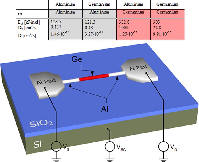
In this Letter we report on the exploration of axial metal/semiconductor (Al/Ge) nanowire heterostructures with abrupt interfaces. The formation process is enabled by a thermal induced exchange reaction between the vapor–liquid–solid grown Ge nanowire and Al contact pads due to the substantially different diffusion behavior of Ge in Al and vice versa. Temperature-dependent I–V measurements revealed the metallic properties of the crystalline Al nanowire segments with a maximum current carrying capacity of about 0.8 MA/cm2. Transmission electron microscopy (TEM) characterization has confirmed both the composition and crystalline nature of the pure Al nanowire segments. A very sharp interface between the ⟨111⟩ oriented Ge nanowire and the reacted Al part was observed with a Schottky barrier height of 361 meV. To demonstrate the potential of this approach, a monolithic Al/Ge/Al heterostructure was used to fabricate a novel impact ionization device.
Keywords: Nanowire, heterostructure, Schottky contact, germanium, aluminum, impact ionization
Nanowires (NWs) synthesized from various semiconducting materials have become a promising field of research, opening up substantial opportunities for a wide range of novel nanoscaled devices including optical,1 electronic,2 and biotechnological3 applications. Within the bottom-up paradigm for nanotechnology,4,5 this is, among others, accounted by the flexible and versatile vapor–liquid–solid (VLS) growth mechanism6 enabling customization of NW properties such as geometry, composition, or crystal orientation. Many of the aforementioned applications benefit from heterostructures, i.e., the combination of two or more materials stacked laterally or axially within the same NW structure.7 The interactions within such quasi-one-dimensional heterostructures and their interfaces can give rise to electronic or photonic characteristics that are superior to those of planar geometries.8 A particular advantage unique to NWs is the potential of lateral strain relaxation,9 mitigating the limitations of material lattice compatibility and allowing arbitrarily combined dissimilar materials unattainable in layered structures. Such axial heterostructures combining metal and semiconductor NWs are among others foreseen as integrated contact and interconnection solutions for nanometer-scale electronic building blocks.10−12 In Si and Ge NWs such silicide/Si and germanide/Ge heterostructures are usually formed by a phase transformation process induced by thermal annealing.13−16 Thereby, metals, e.g., nickel,17 copper,18 or platinum13,14 diffuse from a lithographically defined contact pad into the Si/Ge NW and convert a section of it into the respective silicide/germanide. This enables low-resistance electrical contacts and allows defining field effect transistor (FET) channel lengths smaller than those defined with lithographic techniques.15,16 However, these quasi-metallic structures still exhibit higher resistivity compared to pure metals.13,14,18
In this Letter we show for the first time the formation of single crystal metal/semiconductor (Al/Ge) NW heterostructures with abrupt interfaces. To demonstrate the potential of this approach, we fabricated a novel impact ionization device utilizing fully CMOS-compatible technology.
For this study ⟨111⟩ oriented Ge NWs were grown heteroepitaxially on silicon substrates in a low-pressure chemical vapor deposition system by the use of the gold assisted VLS process.19 The NWs were dispersed on highly p-doped Si substrates with a 100 nm thick dielectric layer of thermally grown SiO2. Afterward Al contacts were formed with e-beam lithography, sputter deposition, and lift-off techniques. The formation of the axial Al/Ge NW heterostructure was achieved by thermal annealing at 623 K in forming gas. The scanning electron microscopy (SEM) image in Figure 1a shows dark segments emerging from the Al contact pads, which prolonged along the Ge NW during the annealing. These segments appeared to be pure and crystalline Al. The extension of these Al segments and accordingly the length L of the remaining Ge NW segment (∼750 nm in Figure 1a) critically depend on the annealing temperature, time, and the diameter of the pristine Ge NWs (see Supporting Information). This successive exchange of Ge by Al due to annealing can be monitored and even controlled in situ in a SEM system equipped with a heating stage (Supporting Information). Thus, by controlling the remaining length of the Ge NW segment, back-gated Ge NW FETs with various channel length and Al source/drain contacts can be fabricated (see Figure 1b).
Figure 1.
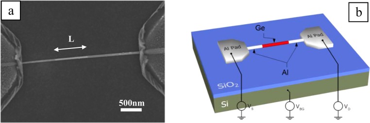
(a) SEM image of the Al/Ge/Al NW heterostructure with an unreacted Ge segment of L = 750 nm. (b) Schematic illustration of the contacted NW heterostructure resembling a back-gated Ge NW FET with SiO2 (tox = 100 nm) as gate dielectric and Al as the S/D contact metal.
To investigate the crystal structure and elemental distribution of the Al and Ge segments, as grown NWs were dispersed on 50 nm thick silicon nitride TEM membranes. After Al pad formation the samples were annealed at 623 K for 240 s in forming gas atmosphere. Furthermore, samples were heated inside the TEM, and the phase formation was imaged in real time. After propagation of the Al phase, the heating was stopped and chemical analysis was performed on the interface. TEM was performed on an FEI Osiris microscope equipped with SuperX EDX detector for chemical analysis working at 120 kV and an FEI TECNAI F20. Figure 2 summarizes the results obtained on both types of samples. Figure 2a shows a high-angle annular dark field (HAADF) scanning transmission electron microscopy (STEM) image made at the Al/Ge interface. The contrast in HAADF STEM depends both on the sample thickness and on its composition where the more heavy elements scatter more electrons on the annular detector, giving rise to a brighter contrast. Clearly a strong chemical contrast is present with a high intensity on the unreacted Ge part of the NW and a much lower intensity on the reacted part. Since the NW diameter does not change noticeably over the interface, this strong contrast change indicates the presence of heavy elements on the unreacted side, which would correspond to Ge (Z = 32) and a high Al content (Z = 13) that is a much lighter element on the reacted side. Figure 2b shows a high resolution HRTEM micrograph of the respective Ge/Al NW heterojunction.
Figure 2.
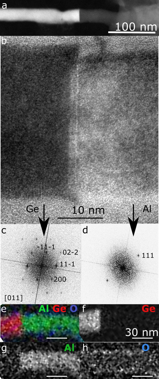
(a) HAADF STEM and (b) HRTEM image of the Ge/Al heterojunction and (c) the respective indexed FFT patterns of the Ge and (d) Al segments. (e–h) EDX mapping of the Al/Ge interface, presenting (e) RGB elemental map of Ge, Al, and O and (f) the Ge, (g) the Al, and (h) the O map, respectively.
The interface appears to be very sharp and both partitions of the NW crystalline as atomic planes are visible in the HRTEM image (Figure 2b). The Ge part of the NW was oriented on the [011] direction of observation and the corresponding reciprocal lattice peaks obtained from the Fourier transformation (Figure 2c) show the ⟨111⟩ growth direction of the Ge NW segment with the diamond cubic structure and a lattice constant of 0.566 nm being in good agreement with tabulated values.20 The Fourier transformation in the reacted part shows only one family of planes, with a spacing of 0.236 nm, in good agreement with the theoretical interplanar spacing of 0.234 nm for ⟨111⟩ planes in face centered cubic (fcc) Al.21 To confirm the composition of the reacted part, energy dispersive X-ray analysis (EDX) was performed in situ in the TEM directly after the propagation of the Al phase inside the Ge NW. The EDX maps in Figure 2e–h show that the darker part in the HAADF STEM image (Figure 2a) of the NW consists of pure Al and the brighter part is pure Ge. Since the EDX analysis was performed directly after the formation of the heterostructure, no effects of aging could occur, potentially modifying the results. Ex situ EDX experiments carried out on previously reacted samples allowed us to confirm that the reacted part of the NW is pure Al and only very low Ge concentrations of a few atomic percent can be detected in very thin (2 nm and less) radial shells around the pure Al core; these results will be published elsewhere. Therefore, the analysis of the crystal structure in the reacted part as well as the elemental analysis, support the hypothesis that Ge is entirely replaced by Al in the reacted part of the NW creating an Al/Ge heterostructure. The Al/Ge interface appears very sharp and might be atomically abrupt (Figure 2a,b). In the HRTEM image (Figure 2b) the interface appears to extend over a few atomic planes. This observation could be explained by a projection effect: the Al phase appears to be more advanced into the NW in the center than on the surface of the NW, and in projection, the top and bottom surface of the NW could give this impression of a less than atomically sharp interface. However, we have observed that these structures are prone to beam damage introduced by the high energy electron beam in TEM and also some aging can occur if the structures remain exposed to ambient air.
The formation of this metal/semiconductor NW heterostructure can be discussed straightforward by examining the Ge–Al phase diagram and considering the substantially different diffusion behaviors of Ge in Al and vice versa. The binary Ge–Al phase diagram is of the simple eutectic type with no intermetallic phase formation.22 The melting points of Al and Ge are 933 and 1211 K, respectively, and the eutectic point is located at a Ge composition of about 29.5 atom % with solid to liquid transition at 693 K. At the particular processing temperature of 623 K, Al shows a solubility of 0.5 atom % in Ge, while Al can contain up to 1.5 atom % Ge. As listed in Table 1 the diffusion constants for both, Ge and Al in Al at 623 K are considerable, i.e., 1012 times larger than in Ge.23,24
Table 1. Activation Energy and Diffusion Coefficients23,24 for Ge and Al and Thereof Calculated Diffusion Lengths S at the Annealing Temperature of 623 K and a Processing Duration of 360 s.

Thus, Ge from the interface can effectively diffuse into the Al contact pad. In contrast to the Kirkendall effect,25 which occurs when one element diffuses more quickly than the other and the lattice sites left behind are empty26 for that particular system, Al is effectively supplied via fast self-diffusion and released to the Ge NW for the compensation of the Ge diffusion. The actual diffusion lengths S (see Table 1) calculated for the selected process conditions are in good agreement with our experimental observations. Controlling the process parameters, particularly the duration of the annealing, Al/Ge/Al NW heterostructures with defined length of the Ge segment can be fabricated.
The exchange reaction also took place when the whole structure was covered by Al2O3 excluding surface diffusion and evaporation effects (Supporting Information). Thereby in accordance with the phase diagram, Ge substitution at the interface continues as long as the Ge concentration in Al is below the solubility limit. This was demonstrated for very small Al pads as the exchange reaction, i.e., Ge replacement, comes to a standstill when the Ge concentration in Al surpasses the 1.5 atom % limit regardless of further annealing (see Supporting Information). Remarkably, in the remaining Ge NW segment no Al contamination can be detected due to the extremely low diffusion coefficient of Al in Ge. Accordingly, extended Al pads of several 100 × 100 μm2 represent a huge reservoir for Ge, and the reaction is prolonged as long as the process temperature is high enough. Thus, by patterning adequate Al pads on both sides of the Ge NW we even accomplished full exchange of the Ge resulting in a pure Al NW keeping the geometry of the former Ge NW. Such fully exchanged NWs appear to be single crystalline Al in the HRTEM micrographs, and energy dispersive TEM-EDX measurements revealed that they are free of Ge in the Al core in the detection limit of typically 0.5 atom %.
To investigate the electrical transport properties of such fabricated crystalline Al NWs and axial Al/Ge/Al NW heterostructures we performed temperature-dependent I–V and common back-gated FET characterization measurements. The I–V characteristic of a fully exchanged, i.e., pure Al, NW in the upper left inset of Figure 3 reveals a perfect ohmic behavior with a resistivity of about 0.5 μΩ m at room temperature, about 20 times higher than the tabulated value of bulk Al.24 As expected for a metallic NW the resistivity increases monotonically with temperature (see Supporting Information). The maximum current density before immediate electrical breakdown was determined to be about 0.8 MA/cm2 close to conventional conductors, such as Cu, Al, Au, and Ag (∼1 MA/cm2).27−32 The main plot in Figure 3 shows the I–V characteristic for an Al/Ge/Al NW heterostructure with a total length of 1.5 μm and an unreacted 750 nm long and 40 nm thick Ge NW segment. The current at room temperature (300 K) appeared to be five orders of magnitude lower in comparison to the fully exchanged Al NW although the bias voltage is 1000 times greater. Further the current decreases with decreasing temperature indicating that the semiconducting Ge NW segment determines the electrical properties of the overall NW heterostructure. The observed antisymmetric nonlinear current voltage relationship corresponds to two back-to-back Schottky diodes in series with the resistance of the NW (lower right inset in Figure 3), which is commonly addressed to explain nonlinear I–V curves of semiconductor NW devices.33 Assuming thermionic emission, the Schottky barrier height (SBH) of the Al/Ge interface can be obtained from the slope of the activation energy plot of ln(I/T2) versus 1/T at various bias voltages shown in the lower right inset in Figure 3.34 A thereof calculated SBH of 361 meV is about 160 meV above the theoretical value of 200 meV, which is shown in the band diagram in the inset in Figure 3 but in good agreement with other measurements35 indicating a strong Fermi level pining for Ge Schottky contacts around 400 meV.36
Figure 3.
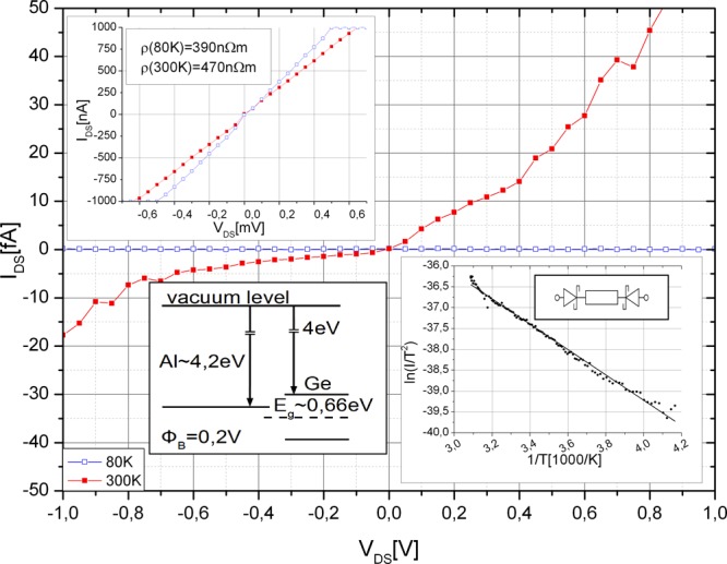
I–V characteristic of the Al/Ge/Al NW heterostructure (main plot) and fully exchanged Al NW (upper left inset) measured at RT (red line) and 80 K (blue line), respectively. The lower left inset shows the band relation between Al and intrinsic Ge. The lower right inset shows the activation energy plot ln(I/T2) as a function of inverse temperature for an individual Al/Ge/Al NW heterostructure and the respective model of the circuit diagram.
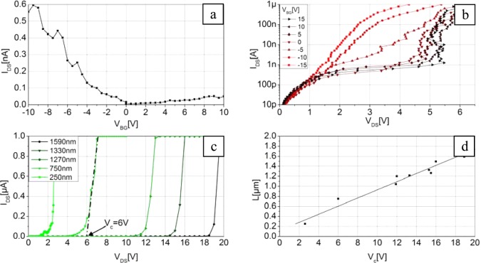
As schematically shown in Figure 1b such an Al/Ge/Al NW heterostructure on top of an oxidized wafer resembles an FET in back-gated configuration with the SiO2 layer (tox = 100 nm) as gate dielectric and highly conductive Al as the S/D contact metal. Figure 4a shows a typical transfer (IDS–VBG) characteristic of the Ge NW FET. With increasing negative gate voltage the current through the NW increases appreciably, characteristic for a p-channel enhancement mode transistor. The VLS synthesized NWs are not doped on purpose during growth, but due to surface states and bulk impurities unintentional p-type doping of Ge NWs usually occurs.37,38 More remarkably, for positive back gate voltages, the semilog plot of the output characteristic in Figure 4b, clearly shows two different slopes. The extremely steep transition from low current values to the compliance setting of 1 μA is considered as the onset of impact ionization.39,40 This transition appears to be critically dependent on the length of the Ge segments. The I–V characteristics measured at an extended voltage sweeping range up to 20 V at VBG = 15 V showed the steep transition from low current values to the compliance setting at different VSD (see Figure 4c). A critical voltage VC was introduced as the value of the linear fit’s zero-line crossings, highlighted in Figure 4c for the segment with L = 750 nm. As expected VC strictly depends on the length of the Ge segment, namely, that VC decreases with decreasing Ge NW length. This is obvious as the critical field at the onset of impact ionization was considered to remain approximately constant. The dependence of VC onto L is shown in Figure 4d. A thereof calculated critical field of about 80 kV/cm is in line with the reported break down voltage for bulk Ge with EC of 100 kV/cm.41 Despite the high electric fields, individual segments withstood up to 100 sweeps into the impact ionization regime without any noticeable degradation.
Figure 4.
(a) Transfer characteristic (VDS = 100 mV) and (b) semilog plot of the output characteristic measurement for the Al/Ge/Al NW heterostructure FET device in back-gate configuration with SiO2 (tox = 100 nm) as gate dielectric and Al as the S/D contact metal. (c) Voltage sweeps along Ge segments in the range of L = 250–1590 nm at VBG = 15 V. The compliance current was set to 1 μA to avoid NW damage. (d) Critical field VC for impact ionization as a function of the channel length L.
Our results illustrate that a distinct asymmetry in the diffusion behavior of particular materials enables the postgrowth formation of an epitaxial metal/semiconductor NW heterostructure via thermal annealing. We suppose that this approach should not be limited solely to the materials discussed here, but could apply to other semiconductor/metal couples with an absence of intermetallic phase formation in the phase diagram. Research on quantum mechanical effects, such as tunneling through barriers or carrier confinement effects, in NW heterostructures will greatly benefit from the possibility of forming real metal/semiconductor/metal NW heterostructures as demonstrated in this Letter.
Acknowledgments
The authors gratefully acknowledge financial support by the Austrian Science Fund (FWF) and the technical support by USTEM TU-Wien. The authors further thank the Center for Micro- and Nanostructures (ZMNS) for providing the clean-room facilities.
Supporting Information Available
Detailed description of the experimental procedures. The Supporting Information is available free of charge on the ACS Publications website at DOI: 10.1021/acs.nanolett.5b01748.
Author Contributions
The manuscript was written through contributions of all authors. All authors have given approval to the final version of the manuscript.
The authors acknowledge financial support by the Austrian Science Fund (FWF): project No. I 841-N24 and I 724-N16. We benefited from the access to the technological platform NanoCarac of CEA-Minatech. We acknowledge financial support from ANR programs JCJC (Project COSMOS, ANR-12-JS10–0002).
The authors declare no competing financial interest.
Supplementary Material
References
- Hu L.; Chen G. Nano Lett. 2007, 7113249–3252. [DOI] [PubMed] [Google Scholar]
- Bryllert T.; Wernersson L. E.; Froberg L.; Samuelson L. Electron Device Lett. 2006, 27, 323–325. [Google Scholar]
- Zhang G. J.; Zhang L.; Huang M. J.; Luo Z. H. H.; Tay G. K. I.; Lim E. J. A.; Kang T. G.; Chen Y. Sens. Actuators, B 2010, 1461138–144. [Google Scholar]
- Cui Y.; Lieber C. M. Science 2001, 291, 851–853. [DOI] [PubMed] [Google Scholar]
- Huang Y.; Duan X.; Cui Y.; Lauhon L. J.; Kim K.; Lieber C. M. Science 2001, 294, 1313–1317. [DOI] [PubMed] [Google Scholar]
- Wagner R. S.; Ellis W. C.; Jackson K. A.; Arnold S. M. J. Appl. Phys. 1964, 35102993–3000. [Google Scholar]
- Johansson J.; Dick K. A. CrystEngComm 2011, 13, 7175. [Google Scholar]
- Hyun J. K.; Zhang S.; Lauhon L. J. Annu. Rev. Mater. Res. 2013, 43, 451–479. [Google Scholar]
- Larsson M. W.; Wagner J. B.; Wallin M.; Håkansson P.; Fröberg L. E.; Samuelson L.; Wallenberg L. R. Nanotechnology 2007, 18, 01550. [Google Scholar]
- Weber W.; Geelhaar L.; Graham A.; Unger E.; Duesberg G.; Liebau M.; Pamler W.; Cheze C.; Riechert H.; Lugli P.; Kreupl F. Nano Lett. 2006, 6, 2660–2666. [DOI] [PubMed] [Google Scholar]
- Appenzeller J.; Knoch J.; Tutuc E.; Reuter M.; Guha S. Electron Devices Meeting IEDM ’06 International 2006, 1–4. [Google Scholar]
- Wu Y.; Xiang J.; Yang C.; Lu W.; Lieber C. M. Nature 2004, 430, 61–65. [DOI] [PubMed] [Google Scholar]
- Liu B.; WangY; Dilts S.; Mayer T. S.; Mohney S. E. Nano Lett. 2007, 73818–824. [DOI] [PubMed] [Google Scholar]
- Lin Y. C.; Lu K. C.; Wu W. W.; Bai J.; Chen L. J.; Tu K. N.; Huang Y. Nano Lett. 2008, 83913–918. [DOI] [PubMed] [Google Scholar]
- Lu K.; Wu W.; Wu H.; Tanner C.; Chang J.; Chen L.; Tu K. Nano Lett. 2007, 7, 2389–2394. [DOI] [PubMed] [Google Scholar]
- Hu Y.; Xiang J.; Liang G.; Yan H.; Lieber C. M. Nano Lett. 2008, 8, 925–930. [DOI] [PubMed] [Google Scholar]
- Katsman A.; Yaish Y.; Rabkin E.; Beregovsky M. J. Electron. Mater. 2010, 394365–370. [Google Scholar]
- Burchhart T.; Lugstein A.; Hyun Y. J.; Hochleitner G.; Bertagnolli E. Nano Lett. 2009, 9113739–3742. [DOI] [PubMed] [Google Scholar]
- Burchhart T.; Lugstein A.; Hyun Y. J.; Hochleitner G.; Bertagnolli E. Nano Lett. 2009, 9113739. [DOI] [PubMed] [Google Scholar]
- D’Ans J.; Lax E.; Blachnik R.. Taschenbuch für Chemiker und Physiker/D’Ans; Springer: Berlin Heidelberg, 1998. [Google Scholar]
- Owen E.; Yates E. J. Chem. Phys. 1935, 3, 605. [Google Scholar]
- McAlister A.; Murray J. Bull. Alloy Phase Diagrams 1984, 54341–347. [Google Scholar]
- Beke D.Landolt-Bornstein: Group III Condensed Matter; Springer: Berlin Heidelberg, 1998; Vol. 33A. [Google Scholar]
- Gale W.; Totemeier T.. Smithells Metals Reference Book; Elsevier Science: Dordrecht, The Netherlands, 2003. [Google Scholar]
- Kirkendall E. O. Trans. AIME 1942, 147, 104–109. [Google Scholar]
- Shewmon P.McGraw-Hill Series in Materials Science and Engineering; McGraw-Hill: New York, 1969; p 58 [Google Scholar]
- Li P. C.; Young T. K. IEEE Spectrum 1996, 33, 75–78. [Google Scholar]
- Lloyd J. R.; Clement J. J. Thin Solid Films 1996, 262, 135–141. [Google Scholar]
- Tao J.; Cheung N. W. IEEE Electroon. Device Lett. 1993, 14, 249–251. [Google Scholar]
- Preece W. H. P. R. Soc. London 1884, 464–471. [Google Scholar]
- Huntington H. B.; Grone A. R. J. Phys. Chem. Solids 1961, 20, 76–87. [Google Scholar]
- Ho P. S.; Kwok T. Rep. Prog. Phys. 1989, 52, 301–348. [Google Scholar]
- Nam C. Y.; Tham D.; Fischer J. E. Nano Lett. 2005, 5, 2029. [DOI] [PubMed] [Google Scholar]
- Sze S. M.Physics of Semiconductor Devices; Wiley: New York: 1981. [Google Scholar]
- Thanailakis A.; Northrop D. Solid-State Electron. 1973, 16121383–1389. [Google Scholar]
- Nishimura T.; Kita K.; Toriumi A. Appl. Phys. Lett. 2007, 9112123123. [Google Scholar]
- Hanrath T.; Korgel H. A. J. Phys. Chem. B 2005, 109125518–5524. [DOI] [PubMed] [Google Scholar]
- Zhang S.; Hemesath E. R.; Perea D. E.; Wijaya E.; Lensch-Falk J. L.; Lauhon L. J. Nano Lett. 2009, 993268–3274. [DOI] [PubMed] [Google Scholar]
- Grundmann M.The Physics of Semiconductors: An Introduction Including Devices and Nanophysics; Springer: New York, 2006. [Google Scholar]
- Mikawa T.; Kagawa S.; Kaneda T.; Toyama Y.; Mikami O. Appl. Phys. Lett. 1980, 374387–389. [Google Scholar]
- Levinshteĭn M. E.; Rumyantsev S. L.; Shur M.. Handbook Series on Semiconductor Parameters; World Scientific: Singapore, 1996. [Google Scholar]
Associated Data
This section collects any data citations, data availability statements, or supplementary materials included in this article.


