The development of efficient methods for constructing molecular transport junctions (MTJs) with the capability to spectroscopically identify molecules assembled within the junctions continues to challenge the field of molecular electronics.[1,2] Most of the current work in MTJ fabrication relies primarily on ex situ syntheses of molecular wires (e.g. dithiolated molecules) followed by subsequent insertion of the molecules into the gap devices.[3] The problems associated with this approach are: 1) the difficulty involved in synthesizing long molecular wires with thiols on both ends because of the low stability and synthetic yields of these molecules, and 2) complications in bridging the electrodes because of a strong tendency of such molecular wires to aggregate.[4] In addition, the small junction sizes (normally only several nanometers in width) often prohibit the use of routine spectroscopic tools to identify the contents within MTJs. Therefore, a modular method for in situ synthesis of molecular wires to bridge nanogaps[4,5] that allows spectroscopic tracking of the assembly process merits development. Herein, we report a new method to fabricate MTJs using the alkyne-azide “click reaction” within nanogaps fabricated by On-Wire Lithography (OWL), while using surface enhanced Raman scattering (SERS) to characterize the assembly processes within the gaps. This strategy for forming MTJs proceeds in high yields, and, as a result of the accessible functional group requirements of click chemistry, is a modular approach that can be used to form MTJs comprised of different molecular components. Additionally, this approach is well suited for studying transport properties of various molecular architectures because the resulting triazole formed by reacting the alkyne and azide groups retains the conjugation required for the electronic transport.
OWL is an electrochemistry-based nanofabrication technique used to prepare a wide variety of nanowire-based structures (e.g., nanogaps and disk arrays) with control over composition and morphology.[6] The obtained structures have been used for prototyping nanostructured materials with advanced functions in the context of molecular electronics[6–8] and SERS.[9–11] OWL allows one to prepare gaps with feature size control down to 2 nm, which makes them promising testbeds for fabricating MTJs.[7] The characteristics of OWL-fabricated nanogaps include high-throughput and tunable, molecular-sized features. Here, we use click chemistry to demonstrate the in situ modular synthesis of molecular wires within the OWL-generated nanogaps. Click chemistry is a synthetic approach popularized by Sharpless that involves reactions that proceed quickly, with high yields and specificity, under mild conditions.[12] An advantage of forming molecular wires using the click methodology within the OWL-generated nanogaps is that in situ fabrication within a confined space (nanogap) is challenging for other existing testbeds, such as scanning probes,[13–15] and wire crossing[16] because these techniques are not easily solution-processable. Mechanical break junction techniques,[17,18]on the other hand, provide only limited control over gap size in comparison to nanogaps formed by OWL. In this study, the CuI-catalyzed 1,3-dipolar Hüisgen cycloaddition (click reaction) between azides and alkynes (Figure 1c) is utilized as a model reaction for preparing molecular wires within OWL-generated nanogaps to form MTJs.
Figure 1.
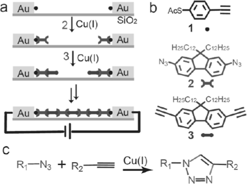
(a) Schematic illustration of click chemistry within the nanogaps. (b) Molecules used in this study. (c) The alkyne-azide “click chemistry” reaction.
The general scheme for bridging the nanogaps with click chemistry for MTJ fabrication is shown in Figure 1a. In a typical experiment, 4-ethynyl-1-thioacetylbenzene (1)[19] is first assembled into a monolayer on the surfaces of the electrodes that are on opposite ends of an OWL-generated nanogap by immersing the entire device in a 1 mM dichloromethane/methanol (2/1, v/v) solution of 1 for 12 hr. 50 µL of concentrated sulphuric acid is added in the solution for thiol deprotection.[20] The device is rinsed with dichloromethane/methanol, chloroform, and ethanol, respectively, and then immersed in a 10 mL DMF solution of 2,7-di-azido-fluorene (2)[21] (1 mM) containing 200 µL of copper sulfate (0.074 M) and ascorbic acid (0.148 M). One of the azides in compound 2 reacts with the alkyne on electrode-immobilized 1 to form a 1,2,3 triazole at one end and unreacted azide at the other end. This structure can be further extended by reaction with 2,7-diethynyl-fluorene (3),[21] which in turn can be reacted again with 2. Following the appropriate number of reaction cycles, the molecular wires growing from opposing electrodes combine and bridge the nanogap. The point at which the bridge is formed can be determined from the I–V characteristics of the device, and the number of reaction steps required to form a bridge depends on the size of the gap.
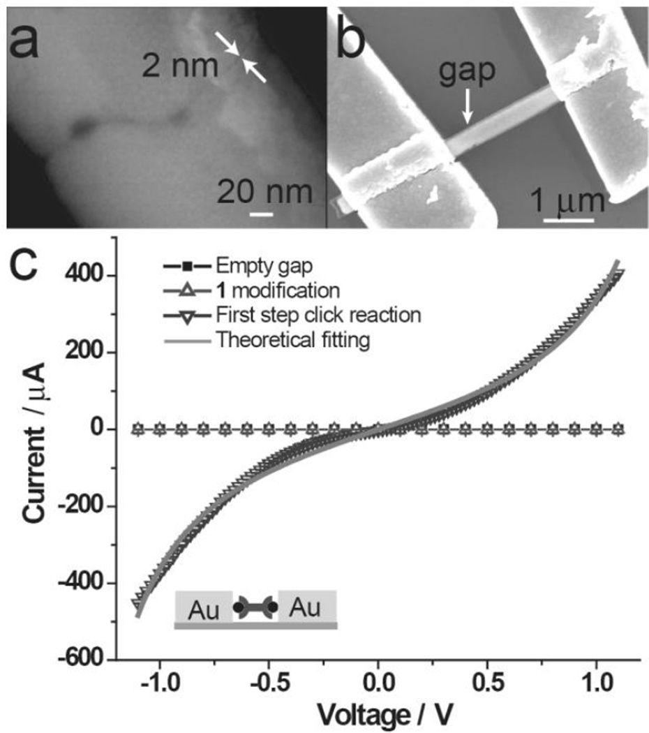
As a proof of concept, we first attempted a one-step click reaction with 1 and 2 to bridge a 2 nm OWL-generated gap and form MTJs. The calculated S-S distance of the target bridging molecule is 2.6 nm, which is long enough to span the gap. In a typical experiment, 360 nm diameter wire structures with 2 nm nanogaps (Figure 2a) were cast onto a substrate with gold microelectrodes and then connected to the electrodes by electron-beam lithography and subsequent chromium and gold thermal deposition (Figure 2b). The two terminal I−V characteristics of the gap devices were measured at room temperature before and after click reactions (Figure 2c). The empty nanogaps or nanogaps modified with only a monolayer of 1 exhibit no conductance within the noise limit of the measurement (<2 pA) (solid square and open uptriangle traces, Figure 2c). However, following the click reaction of 1 and 2 within the gap, I–V characteristics show a clear molecular response in the µA range (open downtriangle trace, Figure 2c), which indicates the realization of a conjugated molecular bridge within the nanogap formed as a result of the click reaction. The yield for working devices is 41% (12 out of 29 devices with I >0.1 nA at 1 V bias). It should be noted that the magnitude of the current measured with different devices varies from 0.1 nA to 600 µA at 1 V bias, which is presumably results from different numbers of molecules bridging the nanogap in different experiments (Figure S5). It is also likely that the roughness of the electrode surface contributes to the observed variation. As a control experiment, we synthesized the dithiol 4 (see supporting information for structure) ex situ from 1 and 2, and the current amplitude and yield of working devices is lower (~10%, 3 out of 31) than that of MTJ devices assembled in situ. This observation likely results from the slow diffusion of the large molecule into the nanogap.[11]
Figure 2.
(a) An SEM image of 2 nm OWL-generated nanogap. (b) An SEM image of 2 nm nanogap-MTJ device. (c) Representative I–V response for 2 nm OWL-fabricated gaps before (solid square curve), after (open uptriangle curve) being modified with 1, and the bridging click reaction of 2 with 1 (open downtriangle curve). Theoretical fitting I–V curve.
X-ray photoelecton spectroscopy (XPS) of a proof-of-concept system on a bulk surface confirmed that the click reactions proceed on gold. For example, the assembly of 1 and the click reaction between 1 and 2 were carried out on a planar gold substrate surface (model system) and followed by XPS in the S 2p region and the N 1s region. In general, the S 2p spectra are composed of 2p3/2 and 2p1/2 peaks with an intensity ratio of 2:1, as theoretically determined from the spin-orbit splitting effect. Figure S3 shows binding peaks at 162.4 (S 2p3/2) and 163.9 eV (S 2p1/2), which are assigned to the bound sulfur.[22] Furthermore, when a surface-bound monolayer of 1 reacts with 2 in the presence of CuI, a peak at 400.2 eV is observed, which arises from the presence of both triazoles and azides (N 1s).[23] These spectral signatures confirm that the 1,3-dipolar cycloaddition between azides and alkynes proceed successfully on monolayer-modified Au surfaces.
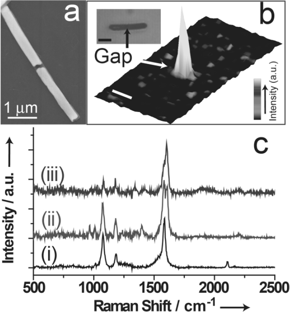
SERS measurements directly on the nanogaps confirm that the click reaction proceeds within this confined space. Sub-100 nm OWL-generated nanogaps have been shown to act as Raman “hot spots” with enhancement factors as large as 108,[9,11] so molecules assembled within nanogaps can be efficiently identified by SERS.[24,25] To evaluate the potential of OWL-generated nanogaps for simultaneous assembly and spectroscopic identification, we fabricated sub-100 nm OWL-generated nanogap structures with gold segments on the opposite sides of the nanogaps. In a typical experiment, a nanogap (98 ± 11 nm) (Figure 3a) was used to assemble the molecules through click chemistry as described for the aforementioned MTJ fabrication, and the Raman spectra and image of the gap area were measured by a confocal scanning Raman microscopy (WiTec Alpha300). For the gap structures modified with 1, the Raman spectrum (i of Figure 3c) clearly shows the presence of alkyne groups (C≡C symmetric stretch at 2108 cm−1) and benzene groups (C-C benzene ring stretching of 1 at 1585 cm−1). In addition, compared with the spectrum of the neat solid of 1 (Figure S6), the absence of thioacetyl (634 cm−1) and SH (bending, 915 cm−1) vibration modes indicates Au-S bonding.[26] The confocal Raman images (Figure 3b) obtained by integrating the spectral intensity from 1520 to 1620 cm−1 and the bright-field optical image shows the hot spots are localized in the gap. When 2 reacts with the monolayer of 1 through click chemistry, new peaks at 967 and 1010 cm−1 (the triazole ring stretch),[27] 1606 cm−1 (C-C benzene ring stretching of 2), and 2198 cm−1 (asymmetric stretching of azide groups) appear, and the peak at 2108 cm−1 disappears (ii of Figure 3c), indicating the click reaction of 1 and 2 proceeded. Furthermore, when 3 reacts with 2 through click chemistry, the relative intensity of the peak at 1606 cm−1 increases (iii of Figure 3c), which confirms the occurrence of the reaction between 3 and 2. These SERS experiments demonstrate the ability to observe directly the chemical reactions within nanogaps and, as a result, confirm the chemical composition of the molecules confined within the MTJs.
Figure 3.
(a) SEM image of an OWL generated nanowire with a 100 nm nanogap. (b) 3D confocal scanning Raman images of an OWL generated gap structure modified with 1. Optical image (inset of b), which is simultaneously obtained, shows the position of the nanogap. Scale bar 2 µm. (c) Representative Raman spectrum taken for the different steps. (i) 1 modified within gap; (ii) following addtion of 2; and (iii) following addtion of 3.
Theoretical calculations were performed to characterize the transport behavior observed across the MTJs. Density functional theory calculations (B3LYP, 6–31G*) were carried out on the gas-phase (geometry optimized) molecular wire, and the HOMO-LUMO gap was determined to be 3.8 eV (HOMO: −5.6 eV, LUMO: −1.8 eV) (Figure S8). In addition, a single level model[28] was used to fit the experimental I–V curve (see supporting information for detail). Assuming transport is in the Landauer regime of coherent tunneling,[29–31] a transport equation dominated by one channel (single level picture) was formulated to obtain the electrode-molecule coupling (0.037 eV on both sides) and the energy gap between the Fermi level and the molecular level (0.75 eV). By taking a gold Fermi level around 5 eV, our results indicate that hole transport (i.e. through the HOMO) dominates. The experimental results (open downtriangle curve, Figure 2c) and theoretical fit (Figure 2c) are in good agreement.
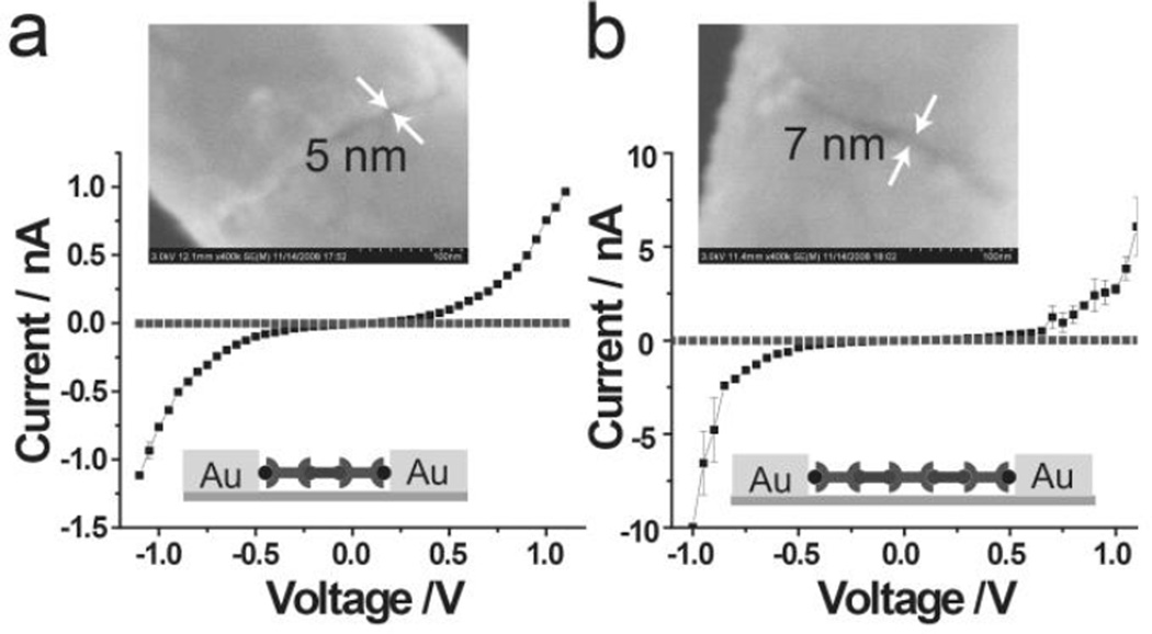
Multistep reactions also can be carried out within the nanogaps in a stepwise approach analogous to solid-phase synthesis. The ability to extend and vary chemical structure within MTJs in situ allows the determination, in a high throughput, combinatorial fashion, of how changes in molecular structure within the gaps affect transport properties. To this end, we have synthesized 3, a fluorene derivative with alkyne substituents. When 3 is reacted with the available azide from 2 on the Au electrode, under click reaction conditions, the oligomeric fluorene chain is extended. This either bridges the gap or leaves an available azide for further reaction (Figure 4). The number of fluorene monomers in the oligomeric chain is controlled precisely by the number of reaction steps and the gap size. We have produced MTJs with three and five fluorene monomers from two and three click reaction steps, in 5 and 7 nm gaps, respectively. Transport is observed only after the appropriate number of reaction steps to bridge the gap have been carried out. In the case of the 5 nm gap, no current is seen until two reactions have been carried out, and in the case of the 7 nm gap, three reactions. These experiments demonstrate the ability to carry out multiple reaction steps within the gap.
Figure 4.
Representative I–V reponse for the multistep click reactions within OWL-fabricated gaps before and after the last step click reaction. (a) 5 nm OWL-gap, two step click reaction; and (b) 7 nm OWL-fabricated gap, three step click reaction.
In summary, we have demonstrated a new method for the in situ, modular fabrication of MTJs through click chemistry in OWL-generated nanogaps whereby the Raman enhancement inherent to these nanostructures is used to spectroscopically characterize the molecular assembly processes within the gaps. The use of click chemistry to form MTJs proceeds in high yields and can be used to test different molecules, and the triazole form maintains conjugation in the molecular wires. In addition, this method overcomes a major challenge in the field of molecular electronics: being able to spectroscopically track the assembly processes of MTJs within such tiny gaps. By using the azide-alkyne click reaction to affix molecules within the gap, the transport properties of different functional building blocks can be explored. We have demonstrated this concept by synthesizing fluorene oligomers of different lengths within the gaps and studying their transport. We anticipate that this new method of forming and characterizing MTJs will be used to create nanoelectronic devices with diverse functions and applications.
Supplementary Material
Footnotes
CAM acknowledges support from the NSF-NSEC. CAM is also grateful for an NSSEF Fellowship from the Department of Defense. ABB is grateful for an NIH Postdoctoral Fellowship. SY is thankful to the ONR for an NDSEG fellowship. MAR acknowledges funding from the MRSEC at NU.
Supporting information for this article is available on the WWW under http://www.angewandte.org or from the authors.
Contributor Information
Mark A. Ratner, Email: ratner@northwestern.edu.
Chad A. Mirkin, Email: chadnano@northwestern.edu.
Reference
- 1.Nitzan A, Ratner MA. Science. 2003;300:1384–1389. doi: 10.1126/science.1081572. [DOI] [PubMed] [Google Scholar]
- 2.Tao NJ. Nat. Nanotechnol. 2006;1:173–181. doi: 10.1038/nnano.2006.130. [DOI] [PubMed] [Google Scholar]
- 3.Tour JM. Acc. Chem. Res. 2000;33:791–804. doi: 10.1021/ar0000612. [DOI] [PubMed] [Google Scholar]
- 4.Taniguchi M, Nojima Y, Yokota K, Terao J, Sato K, Kambe N, Kawai T. J. Am. Chem. Soc. 2006;128:15062–15063. doi: 10.1021/ja065806z. [DOI] [PubMed] [Google Scholar]
- 5.Tang JY, Wang YL, Klare JE, Tulevski GS, Wind SJ, Nuckolls C. Angew. Chem. 2007;119:3966–3969. doi: 10.1002/anie.200604398. Angew. Chem. Int. Ed.2007, 46, 3892–3895. [DOI] [PubMed] [Google Scholar]
- 6.Qin LD, Park S, Huang L, Mirkin CA. Science. 2005;309:113–115. doi: 10.1126/science.1112666. [DOI] [PubMed] [Google Scholar]
- 7.Chen XD, Jeon YM, Jang JW, Qin LD, Huo FW, Wei W, Mirkin CA. J. Am. Chem. Soc. 2008;130:8166–8168. doi: 10.1021/ja800338w. [DOI] [PMC free article] [PubMed] [Google Scholar]
- 8.Qin LD, Jang JW, Huang L, Mirkin CA. Small. 2007;3:86–90. doi: 10.1002/smll.200600386. [DOI] [PubMed] [Google Scholar]
- 9.Qin LD, Zou SL, Xue C, Atkinson A, Schatz GC, Mirkin CA. Proc. Natl. Acad. Sci. U.S.A. 2006;103:13300–13303. doi: 10.1073/pnas.0605889103. [DOI] [PMC free article] [PubMed] [Google Scholar]
- 10.Qin LD, Banholzer MJ, Millstone JE, Mirkin CA. Nano Lett. 2007;7:3849–3853. doi: 10.1021/nl072606s. [DOI] [PMC free article] [PubMed] [Google Scholar]
- 11.Zheng GF, Qin LD, Mirkin CA. Angew. Chem. 2008;120:1964–1967. Angew. Chem. Int. Ed.2008, 47, 1938–1941. [Google Scholar]
- 12.Kolb HC, Finn MG, Sharpless KB. Angew. Chem. 2001;113:2056–2075. doi: 10.1002/1521-3773(20010601)40:11<2004::AID-ANIE2004>3.0.CO;2-5. Angew. Chem. Int. Ed.2001, 40, 2004–2021. [DOI] [PubMed] [Google Scholar]
- 13.Bumm LA, Arnold JJ, Cygan MT, Dunbar TD, Burgin TP, Jones L, Allara DL, Tour JM, Weiss PS. Science. 1996;271:1705–1707. [Google Scholar]
- 14.Cui XD, Primak A, Zarate X, Tomfohr J, Sankey OF, Moore AL, Moore TA, Gust D, Harris G, Lindsay SM. Science. 2001;294:571–574. doi: 10.1126/science.1064354. [DOI] [PubMed] [Google Scholar]
- 15.Xu BQ, Tao NJJ. Science. 2003;301:1221–1223. doi: 10.1126/science.1087481. [DOI] [PubMed] [Google Scholar]
- 16.Kushmerick JG, Holt DB, Pollack SK, Ratner MA, Yang JC, Schull TL, Naciri J, Moore MH, Shashidhar R. J. Am. Chem. Soc. 2002;124:10654–10655. doi: 10.1021/ja027090n. [DOI] [PubMed] [Google Scholar]
- 17.Reed MA, Zhou C, Muller CJ, Burgin TP, Tour JM. Science. 1997;278:252–254. [Google Scholar]
- 18.Reichert J, Ochs R, Beckmann D, Weber HB, Mayor M, von Lohneysen H. Phys. Rev. Lett. 2002;88:176804. doi: 10.1103/PhysRevLett.88.176804. [DOI] [PubMed] [Google Scholar]
- 19.Pearson DL, Tour JM. J. Org. Chem.y. 1997;62:1376–1387. [Google Scholar]
- 20.Cai LT, Yao YX, Yang JP, Price DW, Tour JM. Chem. Mater. 2002;14:2905–2909. [Google Scholar]
- 21.van Steenis DJVC, David ORP, van Strijdonck GPF, van Maarseveen JH, Reek JNH. Chem. Commun. 2005:4333–4335. doi: 10.1039/b507776a. [DOI] [PubMed] [Google Scholar]
- 22.Castner DG, Hinds K, Grainger DW. Langmuir. 1996;12:5083–5086. [Google Scholar]
- 23.Collman JP, Devaraj NK, Eberspacher TPA, Chidsey CED. Langmuir. 2006;22:2457–2464. doi: 10.1021/la052947q. [DOI] [PMC free article] [PubMed] [Google Scholar]
- 24.Tian JH, Liu B, Li XL, Yang ZL, Ren B, Wu ST, Tao NJ, Tian ZQ. J. Am. Chem. Soc. 2006;128:14748–14749. doi: 10.1021/ja0648615. [DOI] [PubMed] [Google Scholar]
- 25.Ward DR, Halas NJ, Ciszek JW, Tour JM, Wu Y, Nordiander P, Natelson D. Nano Lett. 2008;8:919–924. doi: 10.1021/nl073346h. [DOI] [PubMed] [Google Scholar]
- 26.Braun G, Pavel I, Morrill AR, Seferos DS, Bazan GC, Reich NO, Moskovits M. J. Am. Chem. Soc. 2007;129:7760–7761. doi: 10.1021/ja072533e. [DOI] [PubMed] [Google Scholar]
- 27.Yoo BK, Joo SW. J. Colloid Interface Sci. 2007;311:491–496. doi: 10.1016/j.jcis.2007.02.036. [DOI] [PubMed] [Google Scholar]
- 28.Yeganeh S, Galperin M, Ratner MA. J. Am. Chem. Soc. 2007;129:13313–13320. doi: 10.1021/ja0730967. [DOI] [PubMed] [Google Scholar]
- 29.Landauer R. IBM J. Res.Develop. 1957;1:223–231. [Google Scholar]
- 30.Landauer R. Phil. Mag. 1970;21:863–867. [Google Scholar]
- 31.Meir Y, Wingreen NS. Phys. Rev. Lett. 1992;68:2512–2515. doi: 10.1103/PhysRevLett.68.2512. [DOI] [PubMed] [Google Scholar]
Associated Data
This section collects any data citations, data availability statements, or supplementary materials included in this article.


