Abstract
Vertical graphene (VG) nanosheets are directly grown below 500 °C on glass substrates by a one-step copper-assisted plasma-enhanced chemical vapour deposition (PECVD) process. A piece of copper foil is located around a glass substrate as a catalyst in the process. The effect of the copper catalyst on the vertical graphene is evaluated in terms of film morphology, growth rate, carbon density in the plasma and film resistance. The growth rate of the vertical graphene is enhanced by a factor of 5.6 with the copper catalyst with denser vertical graphene. The analysis of optical emission spectra suggests that the carbon radical density is increased with the copper catalyst. Highly conductive VG films having 800 Ω/□ are grown on glass substrates with Cu catalyst at a relatively low temperature.
Electronic supplementary material
The online version of this article (doi:10.1186/s11671-015-1019-8) contains supplementary material, which is available to authorized users.
Keywords: Low temperature, PECVD, Vertical graphene nanosheets, Glass substrate, Copper-assisted growth
Background
Various carbon nanostructures have received enormous attention recently due to their excellent physical properties. For example, graphene, an sp2-hybridized two-dimensional carbon material, shows excellent physical properties in intrinsic mobility [1, 2], mechanical strength [3], optical transmittance [4] and electric conductivity [5]. These properties make graphene a promising material in a wide range of applications of electronics [6, 7], optoelectronics [8, 9], sensors [10, 11], batteries [12] and supercapacitors [13–17]. Enormous processes have been developed for the synthesis of graphene including exfoliation from highly oriented pyrolytic graphite (HOPG), reduction of chemically exfoliated graphene oxide (RGO), thermal decomposition of SiC and chemical vapour deposition (CVD). In general, these processes generate in-plane-oriented monolayer or multi-layer graphene films.
Recently, three-dimensional (3D) graphene attracts attention due to its high surface-area-to-volume ratio [1]. Vertical graphene (VG) nanosheet is one of the popular 3D carbon structure materials [10], which has been applied to various applications of field emitters [7, 18], supercapacitors [19–22] and batteries [23, 24]. In practice, VG films have been typically grown on metal substrates at a relatively high temperature [10, 16], close to 1000 °C, which limits the use of various low-melting-temperature substrates. Yang et al. reported the growth of VG films on dielectric substrates (SiO2) [25] at the temperature of 900 °C. However, the growth rate drops significantly at the temperature below 900 °C. Liu et al. reported the synthesis of carbon nanosheets on a metal-coated glass at a low temperature. In fact, it is a kind of process to grow carbon-based material directly on metal [26]. Recently, the catalytic effect of copper on graphene growth has been reported in high-temperature CVD processes [27, 28], whereas it has not been studied in a plasma-enhanced chemical vapour deposition (PECVD) process. Furthermore, low operation temperature is necessary for an economic and facile process, which can be more feasible for industrial application. Especially, it can pave the way for more applicable substrate materials [29]. For instance, glass is a widely used commercial material with a cheap price but low melting temperature, which should be adopted in a low-temperature process.
In this work, VG films were grown on glass substrates in plasma-enhanced CVD with copper foils at a relatively low temperature, and the properties of vertical graphene films were investigated with the catalytic effect of copper foil in the PECVD process.
Methods
Vertical graphene nanosheets were grown in a radio-frequency (RF) inductively coupled plasma (ICP) reactor as shown in Fig. 1. A piece of copper foil (50 × 25 cm2) was located inside of the quartz tube reactor. The temperature in the centre of the heating area can be increased up to 900 °C by the lamp heater located in the centre of the reactor. A pre-cleaned glass substrate was placed outside (downstream zone) of the direct heating zone, and the temperature around the glass substrates was maintained at about 500 °C to prevent glass deformation. Before the growth of the graphene nanosheets, the glass substrate was cleaned by H2 for 2 min with 100 W of plasma power. After the cleaning, 2 sccm of C2H2 and 1 sccm of H2 were introduced into the tube reactor and 280 W of plasma power was supplied to the coils outside the reactor. The processing pressure was kept at 12 mTorr throughout the growth process. The growth rate was calculated by dividing the height by the growth time from the scanning electron microscopy (SEM) images. After growing graphene nanosheets on the glass substrate, the system was cooled down to room temperature slowly. A uniform VG film obtained on a glass substrate is shown in Fig. 1b.
Fig. 1.
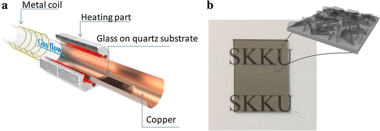
Schematic diagram of the reactor and a photo of the vertical graphene (VG) film. Schematic diagram of the plasma-enhanced chemical vapour deposition (PECVD) reactor (a), and a photo of the VG film deposited on a glass substrate (b)
Optical emission spectra (OES) were taken during the growth process by a high-resolution spectrometer (HR4000CG-UV-NIR, Ocean Optics). The VG film structure was analysed with field emission SEM (JEOL, JSM7401F). High-resolution transmission electron microscopy (HRTEM, JEM-2100F JEOL) was taken to confirm successful growth of graphene in nanoscale. Chemical elements of as-prepared films were determined by an energy-dispersive spectrometer (EDS, JEOL, JSM 6700F). Carbon bonding structure was analysed by Raman spectroscopy (Renishaw, RM-1000 Invia) with a wavelength of 532 nm (Ar+ ion laser). The optical transmittance of VG films was determined by a UV-vis spectrophotometer (UV-650, JASCO) in the visible and infrared ranges.
Results and Discussion
In the process of growing carbon materials by CVD, such as carbon nanotubes and graphene, metal foils (Cu, Ni, Co, etc.) are typically adopted as substrates [7, 20]. However, during the growth process of the VG film by PECVD, we found that the VG films can be also grown on dielectric substrates (e.g. glass) even at temperature as low as 500 °C without any metal substrate, whereas the growth rate is quite low under the low growth temperature. Thus, in order to grow dense VG with a high growth rate, copper was adopted as a catalyst of the low-temperature PECVD process. The significant growth enhancement effect of copper is clearly shown in the SEM images in Fig. 2. Without the copper catalyst, a 100-nm-thick VG nanosheet film is grown in 20 min on a glass substrate (Fig. 2a inset), with a growth rate of 5 nm/min. In this condition, the small VG nanosheets are sparsely spread on the substrate as shown in Fig. 2a. In contrast, a 270-nm-thick VG film is obtained in 12 min with the copper foil inside the reactor. The growth rate is significantly increased to 28 nm/min, and the VG size is enlarged in the copper-assisted PECVD process.
Fig. 2.
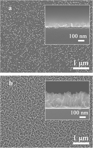
SEM of VG on glass substrate without and with copper catalyst. SEM images of the VG grown on a glass substrate for 20 min without copper catalyst (a) and for 12 min with copper catalyst (b). The inset images are the cross-sectional SEM images of the samples
Several VG films are reported on various substrates of Ni, Si, SiO2 and Cu by PECVD at high temperature [1, 7, 30]. However, the growth mechanism of VG films has not been cleared on glass substrates with copper catalysts. The evolution of VG films on glass substrates is monitored by varying the growth time from 1 to 12 min as shown in Fig. 3. A thin layer is grown on the glass surface within the first 1 min, but no obvious VG nanosheets can be found. The thin layer plays a role as a buffer layer [31], connecting the substrate and the VG nanosheets. The existence of the buffer layer is confirmed by a scratch made by tweezers as shown in the inset. As the growth time is increased to 4 min, a large amount of VG nanosheets appear on the buffer layer (Fig. 3b). As the growth time is increased to 8 and 12 min, the VG nanosheets are further grown and connected densely. The height of the VG nanosheets increases continuously with the growth time (Fig. 3e).
Fig. 3.
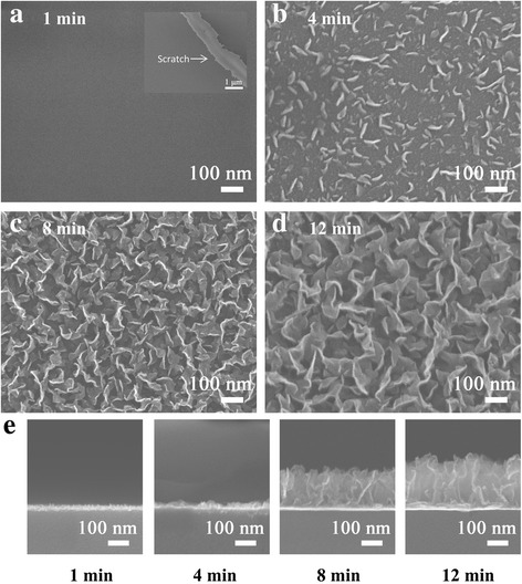
SEM images of growth time effect on VG. SEM images of the VG grown for 1 min (a), 4 min (b), 8 min (c) and 12 min (d). The inset image in (a) shows a scratch made by tweezers. e Cross-sectional SEM images of the VG grown on glass with growth times of 1, 4, 8 and 12 min, respectively
The vertical structure of the crispate VG film was investigated by the cross-sectional SEM analysis as shown in Fig. 4a. The VG film on the glass substrate is composed of two layers of a horizontal buffer layer and VG nanosheets on that buffer layer. The buffer layer is believed to reduce the mismatch of the atomic structure between the glass and VG and similar results observed elsewhere [32], and the VG nanosheets are grown on the buffer layer with less stress. Multi-layer graphene structure in the VG nanosheets was identified by TEM analysis show as shown in Fig. 4b.
Fig. 4.
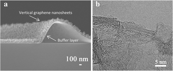
SEM and TEM images of a VG film. a Cross-sectional SEM image of a crispate VG film. b TEM image of a VG nanosheet structure on the VG film. The VG film was grown for 8 min
Raman spectra of the VG films were taken with the different growth time to evaluate the carbon bonding structure as shown in Fig. 5. The VG grown without copper catalyst does not show the characteristic D and G peaks in the Raman spectra within the growth time of 10 min, indicating the deposition of the base layer of amorphous carbon. Until 20 min of the growth time, a carbon layer is deposited and a barely visible (2D) peak can be found at 2670 cm−1. The growth rate is significantly enhanced when the copper catalyst is applied in the PECVD process as shown in Fig. 5b. Significant D and G peaks are observed in the spectrum of the VG film even with a growth processing time of 1 min. However, the low 2D peak signal intensity at 2670 cm−1 implies an amorphous carbon structure [33]. This layer of amorphous carbon is believed to serve as a buffer layer as mentioned earlier. The signal intensity of the 2D peak starts to increase with the increase of the growth time indicating the growth of VG nanosheets on substrate.
Fig. 5.
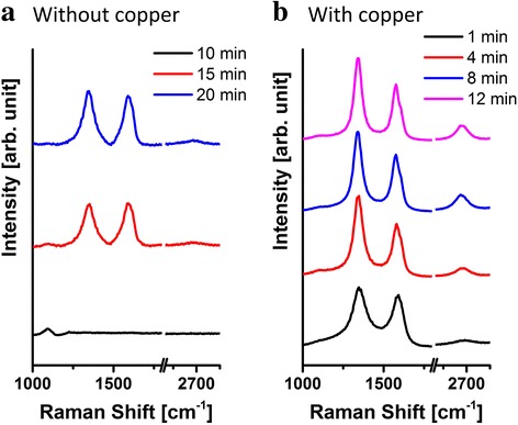
Raman spectra of copper catalytic effect. Raman spectra of VG nanosheets grown without (a) and with (b) assistance of a copper catalyst for different growth times
Based on the above experimental results, the growth mechanism of VG films on the glass substrate in the PECVD system is illustrated in Fig. 6. In the initial stage of VG growth, the hydrocarbon source gas, C2H2, is dissociated into reactive radicals and they are transported onto the glass substrate (Fig. 6a) [34]. A thin layer of amorphous carbon is believed to be formed firstly on the substrate due to the lattice mismatch between the glass and graphene (Fig. 6b) [32]. Then, the graphene nanosheets start to grow, while the amorphous carbon layer is still depositing as well, forming the carbon islands (Fig. 6c). Subsequent in-plane-oriented layer growth mode is unfavourable due to the following three mechanisms: (1) the simultaneous growth of graphene and carbon island leads to discontinuity of horizontal graphene growth; (2) because of the strain energy in the edges and defects of initial graphene, the intermediate layer may not be able to continue to form bulk crystal and thus causes a transition from 2D complete films to 3D clusters [7]; and (3) in this plasma system, the electric field is developed between bulk plasma and the surface of the substrate, and ions generated in plasma are accelerated through the sheath. The energetic ions deliver kinetic energy to the substrate by collisions on the surface, resulting in defects on the graphene film surface helping graphene growth in the vertical orientation (Fig. 6d). The VG growth is unique in plasma-enhanced chemical vapour deposition process and is not observed in typical thermal CVD processes. All these three mechanisms lead to the graphene grown as 3D clusters (Fig. 6e). In the VG growth process with copper catalyst, the hydrocarbon gas molecules are dissociated into reactive radicals on the copper surface [34] and a portion of those reactive radicals is expected to be desorbed from the copper surface and go back to the plasma. Optical emission spectra (OES) were taken during the deposition process to understand the catalytic effect of copper on radical densities as shown in Fig. 7. All the peak intensities increase significantly when the copper catalyst is employed. In particular, the intensities of C2 and CH peaks are quantitatively analysed because C2 and CH radicals have been reported as the major growing source and the terminator of graphene in plasma condition [35, 36], respectively. Thus, the relative intensity of C2:CH can indicate the relative contribution of the growth reaction to termination reaction. As marked in the figure, the relative intensity of C2:CH increases significantly from 0.69 to 1.29 after applying a Cu catalyst. Therefore, the increased reactive radicals contribute to faster formation of the VG film, resulting in the denser and faster growth of VG (Fig. 6f–g).
Fig. 6.
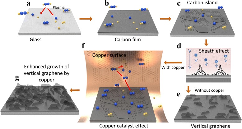
Schematic growth process of VG film on glass substrate in a PECVD system. a Dissociation of carbon-hydrogen bonds by plasma. b Formation of the carbon buffer layer on the glass substrate. c Simultaneous growth of graphene and carbon islands. d Sheath effect and ion bombardment between bulk plasma and the substrate. e Sparse distribution of VG nanosheets prepared by PECVD process without the copper catalyst on the glass substrate. f, g Schematic growth process of the VG film by enhancement of copper catalyst. f Dissociation of hydrocarbon gas on the surface of copper. The dissociated reactive radicals transport to bulk plasma and increase the radical density. g Dense distribution of the VG nanosheets prepared by PECVD process with the copper catalyst on the glass substrate
Fig. 7.
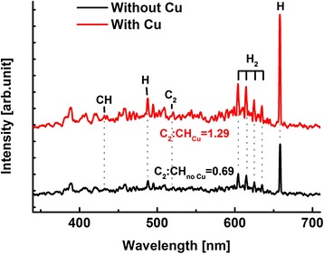
Optical emission spectra (OES) during PECVD process with and without copper catalyst. CH peak was matched at 431.4 nm, C2 peak at 516.5 nm, H peaks at 486.1 and 656.3 nm and H2 peaks at 608.3, 618.8, 624.6 and 628.8 nm. The relative intensity of C2:CH is labelled for the cases with and without a Cu foil
Chemical elements in the VG film were also analysed by EDS in order to detect the presence of copper in the VG samples. As summarized in Table 1 and Additional file 1: Figure S1, no copper element is found in the samples, indicating that the copper works as a catalyst in this PECVD process without being incorporated into the VG films.
Table 1.
Energy-dispersive spectrometer analysis results of VG on glass grown with assistance of a copper catalyst
| Element | Weight % | Atomic % |
|---|---|---|
| C | 10.38 | 16.26 |
| O | 46.61 | 54.80 |
| Na | 6.72 | 5.50 |
| Mg | 2.00 | 1.55 |
| Si | 28.98 | 19.41 |
| Ca | 5.30 | 2.49 |
| Totals | 100.00 |
Finally, the sheet resistance, height and transparency of the VG nanosheets are plotted as functions of growth time as shown in Fig. 8. The transparency of the VG film decreases as the growth proceeds with a longer time (Fig. 8a). Meanwhile, higher VG nanosheets provide lower sheet resistance that can be attributed to the close networking of the VG nanosheets (Fig. 8b). The VG grows with the processing time, but the growth rate is not linear during the whole process. The VG shows a relatively slow growth rate of 10 nm/min in the initial stage within 4 min. As discussed earlier, the base layer is forming in the first minute and VG seeds are forming on the top of the base layer. The VG seeding process may require time and energy. Once the VG seeds are successfully formed on the base layer, the VG grows at the high growth rate of 28.8 nm/min linearly with time in the range of 4 to 12 min.
Fig. 8.
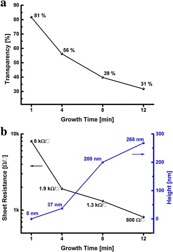
The transparency, sheet resistance and height of VG at various growth times. The transparency as a function of growth time (a) and the sheet resistance and VG nanosheet height as a function of growth time (b)
Conclusions
In this work, vertically oriented conductive graphene film is synthesized directly on glass substrates with a copper catalyst in a low-temperature PECVD process. The catalytic mechanism of copper in the VG growth process is investigated in this work. The transparency and sheet resistance of the VG films were characterized with different growth times. The direct growth of the VG on glass substrates with copper in the PECVD process presented in this work does not require any additional substrate etching or transfer processes. This VG growth process is expected to facilitate the scaleup and makes VG production more economic for potential industrial production. The large surface area of VG films provides a big advantage in the application of electrical devices and energy storage devices.
Acknowledgements
This research was supported by the Basic Science Research Program through the National Research Foundation of Korea (NRF) funded by the Ministry of Education, Science and Technology (2011-0006268). This research was also supported by the MKE (The Ministry of Knowledge Economy), Korea, under the ITRC (Information Technology Research Center)) support program (NIPA-2012-H0301-12-4013) supervised by the NIPA (National IT Industry Promotion Agency).
Additional file
Energy-dispersive spectrometer analysis image of a VG film on glass substrate grown with assistance of a copper catalyst.
Footnotes
Competing Interests
The authors declare that they have no competing interests.
Authors’ Contributions
YM planned the experiment and drafted the manuscript. HJ contributed to the experiments and analysis for OES. SJK, CP and HC revised the manuscript. HC is responsible for project planning. All authors discussed the results and reviewed the manuscript. All authors read and approved the final manuscript.
Contributor Information
Yifei Ma, Email: mayifei@skku.edu.
Haegyu Jang, Email: fromhk@skku.edu.
Sun Jung Kim, Email: kimsj624@skku.edu.
Changhyun Pang, Email: chpang@skku.edu.
Heeyeop Chae, Phone: +82-31-290-7263, Email: hchae@skku.edu.
References
- 1.Bo Z, Yang Y, Chen J, Yu K, Yan J, Cen K. Plasma-enhanced chemical vapor deposition synthesis of vertically oriented graphene nanosheets. Nanoscale. 2013;5(12):5180–204. doi: 10.1039/c3nr33449j. [DOI] [PubMed] [Google Scholar]
- 2.Zhu Y, Murali S, Cai W, Li X, Suk JW, Potts JR, et al. Graphene and graphene oxide: synthesis, properties, and applications. Adv Mater. 2010;22(35):3906–24. doi: 10.1002/adma.201001068. [DOI] [PubMed] [Google Scholar]
- 3.Zhang Y, Tang TT, Girit C, Hao Z, Martin MC, Zettl A, et al. Direct observation of a widely tunable bandgap in bilayer graphene. Nature. 2009;459(7248):820–3. doi: 10.1038/nature08105. [DOI] [PubMed] [Google Scholar]
- 4.Rafiee J, Mi X, Gullapalli H, Thomas AV, Yavari F, Shi Y, et al. Wetting transparency of graphene. Nat Mater. 2012;11(3):217–22. doi: 10.1038/nmat3228. [DOI] [PubMed] [Google Scholar]
- 5.Pang S, Hernandez Y, Feng X, Mullen K. Graphene as transparent electrode material for organic electronics. Adv Mater. 2011;23(25):2779–95. doi: 10.1002/adma.201100304. [DOI] [PubMed] [Google Scholar]
- 6.Bae S, Kim H, Lee Y, Xu X, Park JS, Zheng Y, et al. Roll-to-roll production of 30-inch graphene films for transparent electrodes. Nat Nanotechnol. 2010;5(8):574–8. doi: 10.1038/nnano.2010.132. [DOI] [PubMed] [Google Scholar]
- 7.Jiang L, Yang T, Liu F, Dong J, Yao Z, Shen C, et al. Controlled synthesis of large-scale, uniform, vertically standing graphene for high-performance field emitters. Adv Mater. 2013;25(2):250–5. doi: 10.1002/adma.201203902. [DOI] [PubMed] [Google Scholar]
- 8.Wang X, Zhi L, Mullen K. Transparent, conductive graphene electrodes for dye-sensitized solar cells. Nano Lett. 2008;8(1):323–7. doi: 10.1021/nl072838r. [DOI] [PubMed] [Google Scholar]
- 9.Chen T, Hu WH, Song JL, Guai GH, Li CM. Interface functionalization of photoelectrodes with graphene for high performance dye-sensitized solar cells. Adv Funct Mater. 2012;22(24):5245–50. doi: 10.1002/adfm.201201126. [DOI] [Google Scholar]
- 10.Mao S, Yu K, Chang J, Steeber DA, Ocola LE, Chen J. Direct growth of vertically-oriented graphene for field-effect transistor biosensor. Sci Rep. 2013;3:1696. doi: 10.1038/srep01696. [DOI] [PMC free article] [PubMed] [Google Scholar]
- 11.Liu Z, Robinson JT, Sun X, Dai H. PEGylated nanographene oxide for delivery of water-insoluble cancer drugs. J Am Chem Soc. 2008;130(33):10876–7. doi: 10.1021/ja803688x. [DOI] [PMC free article] [PubMed] [Google Scholar]
- 12.Paek SM, Yoo E, Honma I. Enhanced cyclic performance and lithium storage capacity of SnO2/graphene nanoporous electrodes with three-dimensionally delaminated flexible structure. Nano Lett. 2009;9(1):72–5. doi: 10.1021/nl802484w. [DOI] [PubMed] [Google Scholar]
- 13.Xu Y, Lin Z, Huang X, Wang Y, Huang Y, Duan X. Functionalized graphene hydrogel-based high-performance supercapacitors. Adv Mater. 2013;25(40):5779–84. doi: 10.1002/adma.201301928. [DOI] [PubMed] [Google Scholar]
- 14.Liu C, Yu Z, Neff D, Zhamu A, Jang BZ. Graphene-based supercapacitor with an ultrahigh energy density. Nano Lett. 2010;10(12):4863–8. doi: 10.1021/nl102661q. [DOI] [PubMed] [Google Scholar]
- 15.Wang M, Duong LD, Mai NT, Kim S, Kim Y, Seo H, et al. All-solid-state reduced graphene oxide supercapacitor with large volumetric capacitance and ultralong stability prepared by electrophoretic deposition method. ACS Appl Mater Inter. 2015;7(2):1348–54. doi: 10.1021/am507656q. [DOI] [PubMed] [Google Scholar]
- 16.Wang M, Oh J, Ghosh T, Hong S, Nam G, Hwang T, et al. An interleaved porous laminate composed of reduced graphene oxide sheets and carbon black spacers by in situ electrophoretic deposition. RSC Adv. 2014;4(7):3284–92. doi: 10.1039/C3RA45979A. [DOI] [Google Scholar]
- 17.Yang S, Deng B, Ge R, Zhang L, Wang H, Zhang Z, et al. Electrodeposition of porous graphene networks on nickel foams as supercapacitor electrodes with high capacitance and remarkable cyclic stability. Nanoscale Res Lett. 2014;9(1):672. doi: 10.1186/1556-276X-9-672. [DOI] [PMC free article] [PubMed] [Google Scholar]
- 18.Liu P, Wei Y, Liu K, Liu L, Jiang K, Fan S. New-type planar field emission display with superaligned carbon nanotube yarn emitter. Nano Lett. 2012;12(5):2391–6. doi: 10.1021/nl3003792. [DOI] [PubMed] [Google Scholar]
- 19.Cai MZ, Outlaw RA, Butler SM, Miller JR. A high density of vertically-oriented graphenes for use in electric double layer capacitors. Carbon. 2012;50(15):5481–8. doi: 10.1016/j.carbon.2012.07.035. [DOI] [PubMed] [Google Scholar]
- 20.Bo Z, Wen ZH, Kim H, Lu GH, Yu KH, Chen JH. One-step fabrication and capacitive behavior of electrochemical double layer capacitor electrodes using vertically-oriented graphene directly grown on metal. Carbon. 2012;50(12):4379–87. doi: 10.1016/j.carbon.2012.05.014. [DOI] [Google Scholar]
- 21.Lu X, Wang G, Zhai T, Yu M, Xie S, Ling Y, et al. Stabilized TiN nanowire arrays for high-performance and flexible supercapacitors. Nano Lett. 2012;12(10):5376–81. doi: 10.1021/nl302761z. [DOI] [PubMed] [Google Scholar]
- 22.Bo Z, Zhu W, Ma W, Wen Z, Shuai X, Chen J, et al. Vertically oriented graphene bridging active-layer/current-collector interface for ultrahigh rate supercapacitors. Adv Mater. 2013;25(40):5799–806. doi: 10.1002/adma.201301794. [DOI] [PubMed] [Google Scholar]
- 23.Kim HJ, Wen ZH, Yu KH, Mao O, Chen JH. Straightforward fabrication of a highly branched graphene nanosheet array for a Li-ion battery anode. J Mater Chem. 2012;22(31):15514–8. doi: 10.1039/c2jm33150k. [DOI] [Google Scholar]
- 24.Xiao XC, Liu P, Wang JS, Verbrugge MW, Balogh MP. Vertically aligned graphene electrode for lithium ion battery with high rate capability. Electrochem Commun. 2011;13(2):209–12. doi: 10.1016/j.elecom.2010.12.016. [DOI] [Google Scholar]
- 25.Yang CY, Bi H, Wan DY, Huang FQ, Xie XM, Jiang MH. Direct PECVD growth of vertically erected graphene walls on dielectric substrates as excellent multifunctional electrodes. J Mater Chem A. 2013;1(3):770–5. doi: 10.1039/C2TA00234E. [DOI] [Google Scholar]
- 26.Liu W, Dang T, Xiao Z, Li X, Zhu C, Wang X. Carbon nanosheets with catalyst-induced wrinkles formed by plasma-enhanced chemical-vapor deposition. Carbon. 2011;49(3):884–9. doi: 10.1016/j.carbon.2010.10.049. [DOI] [Google Scholar]
- 27.Teng PY, Lu CC, Akiyama-Hasegawa K, Lin YC, Yeh CH, Suenaga K, et al. Remote catalyzation for direct formation of graphene layers on oxides. Nano Lett. 2012;12(3):1379–84. doi: 10.1021/nl204024k. [DOI] [PubMed] [Google Scholar]
- 28.Kim H, Song I, Park C, Son M, Hong M, Kim Y, et al. Copper-vapor-assisted chemical vapor deposition for high-quality and metal-free single-layer graphene on amorphous SiO2 substrate. ACS Nano. 2013;7(8):6575–82. doi: 10.1021/nn402847w. [DOI] [PubMed] [Google Scholar]
- 29.Kalita G, Wakita K, Umeno M. Low temperature growth of graphene film by microwave assisted surface wave plasma CVD for transparent electrode application. RSC Adv. 2012;2(7):2815–20. doi: 10.1039/c2ra00648k. [DOI] [Google Scholar]
- 30.Miller JR, Outlaw RA, Holloway BC. Graphene double-layer capacitor with ac line-filtering performance. Science. 2010;329(5999):1637–9. doi: 10.1126/science.1194372. [DOI] [PubMed] [Google Scholar]
- 31.Quinlan RA, Cai MZ, Outlaw RA, Butler SM, Miller JR, Mansour AN. Investigation of defects generated in vertically oriented graphene. Carbon. 2013;64:92–100. doi: 10.1016/j.carbon.2013.07.040. [DOI] [Google Scholar]
- 32.Malesevic A, Vitchev R, Schouteden K, Volodin A, Zhang L, Tendeloo GV, et al. Synthesis of few-layer graphene via microwave plasma-enhanced chemical vapour deposition. Nanotechnology. 2008;19(30):305604. doi: 10.1088/0957-4484/19/30/305604. [DOI] [PubMed] [Google Scholar]
- 33.Dresselhaus MS, Jorio A, Hofmann M, Dresselhaus G, Saito R. Perspectives on carbon nanotubes and graphene Raman spectroscopy. Nano Lett. 2010;10(3):751–8. doi: 10.1021/nl904286r. [DOI] [PubMed] [Google Scholar]
- 34.Terasawa T, Saiki K. Growth of graphene on Cu by plasma enhanced chemical vapor deposition. Carbon. 2012;50(3):869–74. doi: 10.1016/j.carbon.2011.09.047. [DOI] [Google Scholar]
- 35.Bhaviripudi S, Jia X, Dresselhaus MS, Kong J. Role of kinetic factors in chemical vapor deposition synthesis of uniform large area graphene using copper catalyst. Nano Lett. 2010;10(10):4128–33. doi: 10.1021/nl102355e. [DOI] [PubMed] [Google Scholar]
- 36.Ma Y, Kim D, Jang H, Cho SM, Chae H. Characterization of low temperature graphene synthesis in inductively coupled plasma chemical vapor deposition process with optical emission spectroscopy. J Nanosci Nanotechnol. 2014;14(12):9065–72. doi: 10.1166/jnn.2014.10098. [DOI] [PubMed] [Google Scholar]


