Abstract
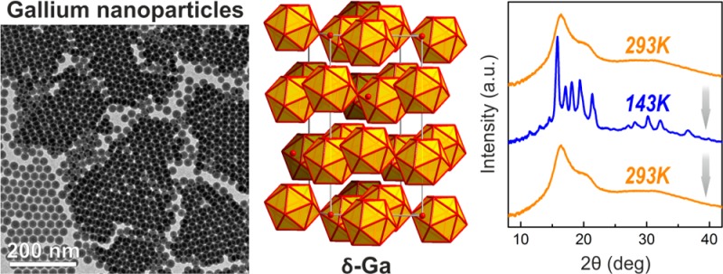
We report a facile colloidal synthesis of gallium (Ga) nanoparticles with the mean size tunable in the range of 12–46 nm and with excellent size distribution as small as 7–8%. When stored under ambient conditions, Ga nanoparticles remain stable for months due to the formation of native and passivating Ga-oxide layer (2–3 nm). The mechanism of Ga nanoparticles formation is elucidated using nuclear magnetic resonance spectroscopy and with molecular dynamics simulations. Size-dependent crystallization and melting of Ga nanoparticles in the temperature range of 98–298 K are studied with X-ray powder diffraction, specific heat measurements, transmission electron microscopy, and X-ray absorption spectroscopy. The results point to delta (δ)-Ga polymorph as a single low-temperature phase, while phase transition is characterized by the large hysteresis and by the large undercooling of crystallization and melting points down to 140–145 and 240–250 K, respectively. We have observed size-tunable plasmon resonance in the ultraviolet and visible spectral regions. We also report stable operation of Ga nanoparticles as anode material for Li-ion batteries with storage capacities of 600 mAh g–1, 50% higher than those achieved for bulk Ga under identical testing conditions.
1. Introduction
Gallium attracts much attention due to its peculiar chemical and physical properties such as strong tendency to Ga–Ga bond formation in solids and in molecules,1 low melting point of just 303 K (29.8 °C),2 rich phase diagram at lower temperatures, (anomalous) volume expansion upon freezing, and numerous technologically relevant alloys and compounds. Chemical stability and surface plasmon resonance (SPR) spanning ultraviolet (UV) and visible spectral regions make Ga nanoparticles (NPs) highly promising for surface-enhanced Raman scattering and for related plasmonic applications.3 The low melting point may enable the use of metallic Ga in all-optical phase-change memory and logic devices4 or as high-capacity self-healing anode in lithium-ion (Li-ion) batteries.5
Previous studies had mainly concerned glass- or polymer-encapsulated Ga nano- and microparticles6 as well as those deposited onto solid substrates via thermal evaporation or by molecular-beam epitaxy.2,3,7 These structures usually contain Ga NPs and nanodroplets larger than 50 nm with size distributions >20%. Much less, however, is known about free-standing colloidal Ga NPs. Arbiol et al.8 have obtained frozen colloids of polydisperse Ga NPs via a gas-phase co-deposition of Ga atoms and molecules of organic solvents (acetone, isopropanol etc.) at 77 K. Several groups observed the formation of Ga NPs as an interim product during the formation of GaAs, GaP, or GaN nanowires and NPs.9 In fact, these latter reports show clear evidence that colloidal Ga NPs may become also a very useful low-temperature catalyst for solution–liquid–solid growth of one-dimensional nanostructures (nanowires, nanorods).10
Here we report a first synthesis of monodisperse colloidal Ga NPs using conventional solution-phase chemistry. Starting with Ga alkylamides as precursors and through the judicious choice of the reaction parameters, we achieved narrow size distributions down to 7–8% and an accurate size control in a wide range of 12–46 nm. Supported by 1H nuclear magnetic resonance (NMR) spectroscopy and by molecular dynamics simulations, we elucidate the mechanism of the conversion of molecular precursors into Ga NPs. Using a set of low-temperature measurements such as transmission electron microscopy (TEM), X-ray diffraction (XRD), specific heat measurements, and extended X-ray absorption fine structure (EXAFS) spectroscopy we perform a comprehensive investigation of structural transitions in gallium NPs in the temperature range of 98–298 K. Reversible and size-dependent crystallization and melting phenomena are observed. In addition, we present a size-dependent SPR in the UV spectral region, which together with high chemical stability makes such Ga NPs highly promising for liquid-metal plasmonic applications. We also report stable operation of Ga NPs as anode material for Li-ion batteries with storage capacities of 600 mAh g–1, close to theoretical capacity and 50% higher than those achieved for bulk Ga under identical testing conditions.
2. Experimental Section
Gallium chloride (GaCl3, 99.999%, anhydrous) and gallium tris(dimethylamide) dimer (Ga2(NMe2)6 99%) were purchased from ABCR; lithium dimethylamide (LiNMe2, 95%), di-n-octylamine (DOA, 98%), di-n-dodecylamine (DDA, ≥ 97%), 1-octadecene (ODE, 90%), and oleic acid (OA, 90%) were obtained from Sigma-Aldrich. DOA, ODE, and DDA were degassed and dried under vacuum at 110 °C for 90 min, cooled to room temperature, and transferred airless to the glovebox. All other chemicals were used as received. The syntheses of Ga2(NMe2)6 and Ga NPs were carried out under inert atmosphere using the glovebox and Schlenk line technique. Post-synthetic purification (“washing”), handling, and storage of Ga NPs were performed under ambient conditions.
Synthesis of Ga2(NMe2)6
This compound was synthesized according to the original protocol of Nöth and Konrad.11 Briefly, LiNMe2 (5.103 g, 0.1 mol) was dissolved in hexane (100 mL) and Et2O (250 mL). This slurry was cooled to 0 °C with an ice–water bath and stirred for 1 h, followed by the dropwise (∼30 min) addition of GaCl3 (5.8 g, 33 mmol) dissolved in Et2O (30 mL). Afterward, the reaction mixture was heated to 40 °C and stirred for 14 h. LiCl and unreacted LiNMe2 were filtered out, and the solvents were evaporated. The yellowish solid was recrystallized twice at −30 °C from the pentane solution, yielding a colorless crystalline product. The purity of Ga2(NMe2)6 was confirmed by 1H NMR spectra.
Synthesis of Gallium NPs
In a typical synthesis of 24 nm Ga NPs, ODE (7 mL) was loaded into a three-neck flask, equipped with the reflux condenser, and dried under vacuum at 110 °C for 1 h. Then the reaction flask was filled with Ar and heated to 280 °C, followed by the injection of solution containing 25 mg of Ga2(NMe2)6 in dried DOA (1.13 mL) and dried ODE (4.87 mL). The temperature dropped to 230–235 °C, and in ca. 1 min the reaction flask was cooled to room temperature. Ga NPs were separated from byproducts and from unreacted precursors by adding chloroform (10 mL), OA (1 mL) and ethanol (20 mL), followed by centrifugation. Ga NPs were redispersed in chloroform, and the purification/precipitation step was repeated 2–3 times. Ga NPs smaller than 30 nm are colloidally stable for at least several months. Larger Ga NPs slowly precipitate upon storage. The reaction can be 4-fold up-scaled, providing similar size and size distribution of Ga NPs. The reaction yield was 30–40%. Experimental details for all other samples of Ga NPs are summarized in Tables S1–S6 and Figures S1–S9.
Electron Microscopy
Philips CM30 TEM microscope operated at 300 kV was used for routine room temperature imaging at low-resolution, and JEOL 2200 TEM microscope operated at 200 kV was used for cryo-TEM experiments and energy dispersive X-ray (EDX) mapping in scanning TEM mode. Large-area EDX spectra were collected on Hitachi S4800 SEM. TEM samples were prepared by dropping a solution of Ga NPs (∼1 mg/mL, in 1,1,2,2-tetrachloroethane) onto standard carbon-coated TEM grids or onto Si4N3 grids for on-grid oxidation experiments. ImageJ software was used to analyze TEM images (size distributions of the samples and intensity line profiles). On-grid oxidation of Ga NPs was carried out using a Fischione 1020 plasma cleaner.
X-ray Diffraction
Low-temperature XRD patterns, used for Rietveld refinement, were collected on Bruker D8 powder diffractometer (Bragg–Brentano geometry, Cu Kα1 radiation, Ge-monochromator, M. Braun PSD-50m detector) equipped with a cooling chamber (Anton-Paar TTK 450). Temperature accuracy of the system is ±15K. Samples were prepared by drying highly concentrated solutions of Ga NPs on glass substrates. Variable-temperature XRD patterns were also taken on Oxford Xcalibur S X-ray diffractometer (Mo Kα radiation, 4-circle kappa goniometer, CCD detector), including Cryojet5 (Oxford Instruments) cryogenic system. Temperature accuracy was ±2–3K. Samples were prepared by mixing solid Ga NPs with small amount of perfluoropolyether (PFO-X175/08, ABCR). This slurry was then mounted on a needle-like Mitegen micromount. Refinement of XRD patterns using Rietveld method was obtained with FullProf Suite software (Laboratoire Léon Brillouin, CEA-CNRS, France). Diamond software was used to visualize the structure of delta (δ)-Ga polymorph.
Solution Phase 1H NMR
Spectra were recorded using a Bruker DRX 500 spectrometer. Spectra were obtained at room temperature with locking. The pulse width was set at 11.4 μs, and the relaxation delay was 1 s. The number of scans used for each experiment was 50. Samples for NMR were prepared in 5 mm tube in glovebox using C6D6 as a solvent. All spectra were referenced to tetramethylsilane.
Specific Heat Measurements
Measurements were performed with a Physical Property Measurement System (PPMS) with the Quantum Design heat-capacity accesory using a relaxation technique.
Extended X-ray Absorption Fine Structure (EXAFS)
Spectra were collected at the SuperXAS beamline (Swiss Light Source, Villigen, Switzerland) around the Ga K-edge (10.367 eV). The incident beam energy was calibrated by setting the monochromator energy to that of the inflection point of a spectrum of a Ta foil (absorption edge is 9.881 eV). Gallium NPs were sandwiched between two Kapton tapes. The temperature was adjusted by a liquid nitrogen stream in the range of 98–298 K. EXAFS spectra were treated with the iFeffit software suite.12 Fourier transformations of the normalized and background-subtracted EXAFS spectra were performed over a k range of 3–10 Å–1. Based on TEM and XRD observations, we assumed that our sample contains 2 phases: a metallic Ga core and an amorphous (native) oxide shell. The EXAFS data were fitted over a R-range of 1.16–4.5 Å by using the first few single scattering paths obtained from theoretical standards for α-Ga and β-Ga2O3 crystal structures.13 Ghigna et al.2 reported a presence of dimeric Ga2 molecules in the liquid Ga and very similar local arrangement of liquid Ga and α-Ga phase. The β-Ga2O3 is a stable room temperature gallium oxide modification. First, we determined the concentration of oxide phase in the Ga NPs solid sample. For this purpose, we performed a fit of the EXAFS spectrum, collected at room temperature, simplifying α-Ga and β-Ga2O3 crystal structures to 4- and 3-shell models, respectively. This allows mimicking all neighbors of an averaged Ga atom up to 4.5 Å. The coordination numbers were taken from the crystal structures and were fixed at their theoretical values (we assumed the NPs to be bulk-like), while bond distances and pseudo Debye–Waller factors (σ2) for each shell were floated independently. Also the overall energy shifts (ΔE0) for the α-Ga and β-Ga2O3 structures and the amplitude reduction factor (S02) were left floating independently. An additional variable x as a contribution of the Ga phase to the EXAFS spectrum was introduced. Temperature-dependent XAS spectra were fitted considering only the closest neighboring shells (R-range of 1.16–3.16 Å). This includes 2 scattering paths for metallic Ga and one Ga–O scattering path for β-Ga2O3. To reduce the number of fitting parameters, the x and S02 parameters and coordination numbers were kept constant for all fits.
Computational Methodology
Ga2(NMe2)6 was considered as an isolated molecular system, whose geometry was optimized at DFT level by using DMol3 code, as implemented in Materials Studio 6.0. The exchange–correlation functional and the dispersion contribution as well as the effective core-potential and the basis set were set as reported elsewhere.14 In addition, the molecular systems were treated as canonical ensembles (NVT) at different temperatures in the molecular dynamics simulations. The results are presented in Figure S11, along with their discussion.
Assembly and Testing of Li-Ion Half-Cells
Electrodes were prepared by ball-milling the ligand-free Ga NPs with carbon black (21 wt %, from Super C65, TIMCAL) and CMC binder (15 wt %, grade: 2200, Daicel Fine Chem Ltd.) in water for 1 h and casting the hereby obtained slurry onto Cu foil. The current collectors were then dried for 12 h at 80 °C. Homemade, reusable coin-type cells were assembled in an argon-filled glovebox (O2 < 1 ppm, H2O < 1 ppm) using Celgard separator (Celgard 2400, 25 μm microporous monolayer polypropylene membrane, Celgard Inc. USA). Li foil served as both reference and counter electrodes. 1 M LiPF6 in ethylene carbonate:dimethylcarbonate (ED:DMC, 1:1 by wt, Novolyte) was used as electrolyte, with the addition of fluoroethylenecarbonate (FEC, 3%) for improving cycling stability. Cells were cycled between 0.02–1.5 V on MPG2 multichannel workstation (Bio-Logic). The obtained capacities were normalized to the mass of NPs.
UV–vis Absorption Spectra
Spectra were acquired for colloidal solutions of Ga NPs in hexane using Carry 5000 UV–vis spectrophotometer.
3. Results and Discussion
Synthesis
In the footstep of recent syntheses of monodisperse Bi, In, and Sn NPs using metal alkyl and silylamides as oxygen-free and highly reactive precursors,14,15 we have selected dimeric tris(dimetylamido)gallium, Ga2(NMe2)6, as a precursor for Ga NPs. Ga2(NMe2)6 is commercially available or can be easily synthesized from GaCl3 using known method.11 We first attempted thermal decomposition in oleylamine (primary amine), a very common high-boiling solvent and surfactant, and observed no decomposition up to at least 300 °C. We therefore eliminated primary amines from the system and used ODE as a high-boiling non-coordinating solvent. Ga2(NMe2)6 readily decomposes in ODE at T = 260–290 °C and in 1–3 min yields Ga NPs with a mean size larger than 50 nm and with broad size distribution of ∼30%. In order to reduce the mean particle size, DOA (secondary amine) was added as a surfactant. The size of Ga NPs can then be varied in the range of 15–46 nm, and size distributions can be optimized down to 7–8% by varying the common synthesis parameters (Figures S1–S7, Tables S1–S5): DOA amount, reaction time, injection and growth temperatures. In addition to TEM images, low-resolution scanning electron microscopy (SEM) images further highlight the high uniformity of NCs in their ensemble (Figure S7). Smaller, 12–15 nm Ga NPs are accessible using bulkier secondary amine, DDA (Figure S8, Table S6).
In a typical synthesis of 24 nm Ga NPs (Figure 1), ODE (7 mL) was dried under vacuum at 110 °C for 1 h and then heated to 280 °C under Ar atmosphere. At 280 °C, a solution containing Ga2(NMe2)6 (25 mg), dried DOA (1.13 mL), and dried ODE (4.87 mL) was swiftly injected, leading to the fast temperature drop to ∼230 °C. The solution turned from yellow to brown 40 s later, indicating the formation of colloidal Ga NPs. In 1 min, the reaction was terminated by cooling to room temperature, and Ga NPs were isolated by a typical solvent–nonsolvent procedure. This injection-based synthesis can be up-scaled by at least a factor of 4, without deterioration of the size distribution (Figure S9).
Figure 1.
An outline of the synthesis of Ga NPs via thermal decomposition of Ga-alkylamides. Dioctylamine acts as a surfactant and also engages into partial or complete transamination of Ga2(NMe2)6, thus controlling the reaction kinetics. (A,B) Low- and high-resolution TEM images of 24.0 nm Ga NPs with narrow size distribution of 7.4%.
Besides the function of DOA as a capping agent for reducing the mean particle size, 1H NMR spectra (Figure S10) suggest one additional role of DOA, which is a displacement of Me2N with Oct2N groups via transamination reaction. Already at room temperature, 1H NMR spectra indicate partial or complete transamination of terminal −NMe2 groups at [DOA]:[Ga2(NMe2)6] molar ratios of 6 and 10, respectively (Figure S10). Complete transamination of terminal and bridging amide groups, which is the formation of Ga-dioctylamide, was observed at higher [DOA]:[Ga2(NMe2)6] ratio of 30. Molecular dynamics simulations (for graphic illustrations and detailed discussion, see Figure S11) were employed to assess the thermal stability of Ga2(NMe2)6 in the presence of DOA and ODE at higher temperatures. Simulations show that while pure Ga2(NMe2)6 decomposes to Ga already at 250 °C, solvation by DOA increases the decomposition temperature further to 300 °C. Furthermore, the product of complete transamination reaction, Ga(NOct2)3, also shows a higher onset of decomposition than Ga2(NMe2)6. The dual effect of the DOA as a surfactant and mild retardant of the precursor reactivity may explain the non-monotonic dependence with a clear minimum in the plots of NP size and size distribution vs amount of DOA (see Figure S1, as an example).
Structural Analysis of Ga NPs
All studied Ga NPs are non-crystalline, presumably liquid at ambient conditions due to low bulk boiling point of just 29.8 °C, as can be seen from conventional high-resolution TEM images (Figure 1B) and from the diffuse rings in the electron diffraction patterns (Figure 2A). This is also apparent from the low-resolution TEM images of NP ensembles (Figures 1A, S12A) showing highly uniform NP-to-substrate contrast, whereas any noticeable crystallinity of NPs would make some NP darker due to diffraction contrast, which depends on the crystal orientation. EDX spectra of Ga NPs point to Ga as the only chemical element present in the sample (Figure S13). A native oxide shell is apparent from the lighter “halo” in TEM images (Figure 1B) as well as from the EDX maps obtained with scanning TEM (STEM, Figure 2E,F).
Figure 2.
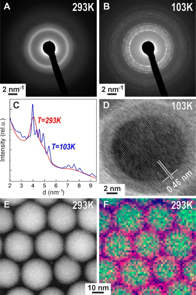
(A,B) Electron diffraction patterns of ∼32 nm Ga NPs at room temperature and at 103 K. (C) Radial integrals of (A) and (B) indicating the appearance of diffraction peaks upon cooling. (D) High-resolution TEM image of a single Ga NP crystalline at 103 K, coated with a native oxide layer. (E) HAADF-STEM, (F) EDX pseudocolor map of Ga NPs, revealing an O-rich thin shell around a Ga core (Ga, green; O, purple).
Reversible, low-temperature phase transitions (melting and crystallization) in low-dimensional Ga can be employed in photonic switches or in optical memory elements which exploit the difference in the optical properties of crystalline and liquid phases.4,16 So far, non-supported colloidal Ga NPs smaller than 50 nm have not been experimentally accessible for structural studies.
Phase transitions of bulk Ga are well documented.17 Besides a low melting point, Ga exhibits rich polymorphism, having 5 crystal modifications at ambient pressure.17a All Ga polymorphs show very peculiar crystal structures such as, for instance, α-Ga containing dimeric Ga2 units18 or γ-Ga containing Ga pentagons and heptagons.19 Upon cooling, liquid Ga films convert into α-Ga at ca. 303 K (29.8 °C).17b Further cooling converts α-Ga first into β, then into δ, ε and γ modifications.17a Previous studies on low-dimensional Ga mainly concerned matrix-encapsulated Ga particles or thermally evaporated thin films or nanoislands on substrates.2,6a,20 The effects of the finite size and high surface energy are the lowering of the temperatures of phase transitions and large hysteresis. Cicco et al. studied submicron Ga particles confined in epoxy resin and showed strong suppression of freezing and melting temperatures down to 150 and 254 K, respectively, and conversion directly into β-Ga polymorph upon freezing, contrary to the liquid → α-Ga → β-Ga sequence in bulk Ga.6a,20d Later, He et al. determined the critical size of ca. 800 nm at which α-Ga is still observed during cooling.20a Smaller Ga NPs exhibit further phenomena such as coexistence of β- and γ-polymorphs in a 100 nm Ga NP grown on the tip of an optical fiber,20f direct freezing of liquid Ga into δ-Ga in 30 nm Ga nanodroplets on silica substrate,2 and liquid state of 10 nm Ga nanodroplets on silica substrate at 90 K.20e
First, we studied the low-temperature crystallization of colloidal Ga NPs deposited onto an amorphous carbon support using TEM microscope equipped with a liquid-nitrogen cooled holder. Electron diffraction patterns, collected upon cooling to 103 K (∼30 min overall cooling time, see also a sequence of diffraction patterns in Movie SI2), provide clear evidence that all studied samples with mean sizes of 12.4, 24.0, 32.4, and 44.0 nm were successfully crystallized (Figures 2B,C and S14). Furthermore, high-resolution images of crystalline Ga NPs (Figure 2D) were also acquired with clearly resolved lattice fringes from crystalline Ga core, surrounded by an amorphous oxide shell. Low-resolution TEM images of an ensemble of Ga NPs (Figure S12B) illustrate diffractional contrast due to random orientation of crystallites. Accurate crystal structure determination was obtained from XRD patterns collected at 113 K, as exemplarily shown for 24 nm Ga NPs in Figure 3. The Rietveld refinement method (FullProf Suite software package, Figure S15)21 reveals that Ga NPs at T = 113 K exist purely in the δ-Ga modification. The δ-Ga polymorph represents one of the most complex single-component crystal structures, containing 66 Ga atoms in the rhombohedral unit cell (R-3m, a = b = 9.087 Å, c = 17.02 Å).22 Most of Ga atoms assemble into hollow icosahedrons, which are interconnected by joint vertices. In turn, these Ga12 polyhedrons are spaced analogously to the arsenic structure type (Figure 3, inset). The refined lattice parameters are very close to those of bulk δ-Ga (a = b = 9.099 Å, c = 17.069 Å). The δ-Ga domain size of 24 nm Ga NPs has been estimated to be ca. 16 nm using Scherrer formula (implemented in Rietveld refinement). This fact stays in a good correspondence with the cryo-TEM measurements (Figure 2D), showing ∼3 nm oxide shell. Importantly, XRD patterns at 113 K and electron diffraction patterns at 103 K can be indexed to δ-Ga phase for all investigated Ga NPs (from 12 to 46 nm). These temperatures are in fact much lower than the known stability region of bulk δ-Ga polymorph (246–253 K).17a
Figure 3.
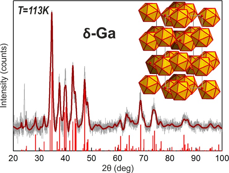
Wide-angle powder X-ray diffraction pattern (Cu Kα1 irradiation) for 24 nm Ga NPs at 113 K presented together with theoretical pattern for δ-Ga and a fit obtained by Rietveld refinement. Inset illustrates a crystal structure of δ-Ga polymorph.
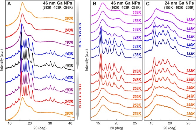
In order to have a closer insight into the crystallization and melting temperatures, a series of XRD patterns was collected in the temperature range of 103–293 K for two sizes of Ga NPs: 24 and 46 nm (Figures 4, S16). For efficient heat exchange, Ga NPs were mixed with perfluoropolyether, and the resulting slurry was then tipped onto the Kapton needle, while the cooling/heating is achieved with focused stream of nitrogen. The first temperature sweep with large 50K steps (Figures 4A and S16, 46 and 24 nm Ga NPs) allows localizing the regions of melting and crystallization. Then within these regions XRD patterns were recorded every 2–3 K (Figure 4B, C). XRD patterns for 24 and 46 nm Ga NPs show hysteresis of ∼100 K and indicate weaker size dependence for crystallization (143–148 K for 46 nm Ga NPs and 140–145 K for 24 nm Ga NPs) and more-pronounced size effect during the melting (253–255 K for 46 nm Ga NPs and 240–245 K for 24 nm Ga NPs). In all experiments only δ-Ga polymorph was observed. Importantly, crystallization and melting are fully reversible, as has been observed by repeated cooling and heating (Figure S17).
Figure 4.
Temperature-dependent XRD (Mo Kα) patterns for Ga NPs. (A) Rough scan over the temperature range of 103–293 K for 46 nm Ga NPs. (B,C) More detailed study near the temperatures of phase transitions for 24 and 46 nm Ga NPs.
Reversible crystallization of Ga NPs can be followed also by specific heat measurements (Figure 5), a standard technique for observing first- and second-order phase transitions. Distinct discontinuities from linear behavior are observed at 242 K (while heating) and 155 K (while cooling) for 24 nm Ga NPs. An important hint from specific heat measurements is that the crystallization region is broader than the sharp melting transition. A broad feature at 210–220 K upon heating (before melting) can be attributed to the surface premelting of Ga NPs. Rühm et al.23 reported that premelting processes in bulk Ga appear ∼10 K below the melting point. During premelting, a liquid shell grows up to about seven atomic layers prior to the fast and complete melting.23 Considering the large specific surface of Ga NPs, the premelting phenomenon may become significant. An evidence of premelting can also be conceived from the XRD patterns as well: 248 and 253 K patterns for 46 nm Ga NPs or 233, 238, and 240 K patterns for 24 nm Ga NPs (Figure 4B,C) show broadening of Bragg reflections with the temperature increase before the crystallinity sharply disappears.
Figure 5.
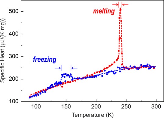
Temperature-dependent specific heat measurements for 24 nm Ga NPs.
EXAFS Spectroscopy
In contrast to X-ray diffraction, EXAFS spectroscopy can accurately probe the local structure of non-crystalline samples (i.e., amorphous shell, liquid state). In this study, we recorded the Ga K-edge EXAFS spectra for Ga NPs at every 50 K step while cooling from 298 to 98 K and then during heating back to room temperature. EXAFS spectroscopy provides the local geometric structure around Ga atoms, including identity of nearest neighbors and bond distances as well as percentage of amorphous oxide phase present. The best fits of the room-temperature EXAFS spectra (Figure S18 and Table S7) revealed the concentration of Ga2O3 in the 24 nm Ga NPs sample to be ∼17 at. %, which corresponds to ∼2 nm Ga 2O3 shell thickness around a 20 nm metallic Ga core. We also noted that the room-temperature Ga–Ga distances in the metallic NP core are slightly smaller than known values for α-Ga structure.18 This fact can be attributed to the higher density of liquid Ga as compared to the solid α-Ga phase (so-called ice-like behavior of Ga, i.e., a volume expansion upon freezing). Similar observations were reported by Ghigna et al.2 The Ga–O distances are in good agreement with the β-Ga2O3 crystal structure (Table S7).
The temperature-dependent EXAFS spectra are shown in Figure S19 together with the best fit curves. Figure 6 represents the extracted Ga–Ga distances for two averaged Ga shells. Abrupt changes of Ga–Ga distances happen between 148 and 98 K upon cooling and between 198 and 248 K upon heating. Being in good correspondence to other methods, these changes are attributed here to freezing and melting phase transitions of Ga NPs. The Ga–Ga distances in metallic Ga at T = 98, 148 (during heating), and 198 K (during heating) match well with the Ga–Ga distances in the δ-Ga crystal structure (Table S8 and ref (22)). For all other temperatures, the Ga–Ga distances remain smaller than that of α-Ga, confirming the liquid state of Ga NPs. Overall, the combined results of XRD, TEM, specific heat, and EXAFS measurements point to a strong tendency to overcooling, a large hysteresis between crystallization and melting and the absence of the stable α-Ga modification but formation of only δ-Ga polymorph for crystallized Ga NPs in the studied size range of 12–46 nm.2,4c,6a,20a−20c
Figure 6.
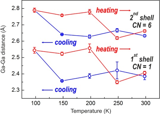
Ga–Ga distances for two shells, extracted from the best fits of EXAFS spectra at different temperatures. CN is coordination number.
Surface Plasmon Resonance in UV Region
The current research in metallic plasmonics, including potential applications such as surface-enhanced Raman spectroscopy (SERS), metal-enhanced fluorescence, chemical sensing, and information storage, is largely concentrated on gold and silver nanostructures, whose SPR spans over the entire visible and near-IR regions of up to ∼1500 nm.24 For the UV plasmonics, Ga NPs may become one of the best candidates due to the high bulk plasmon energy of 13.9 eV, good chemical stability, size-tunable liquid state and broad temperature range of the stability of the plasmon resonance from −80 to 600 °C, and SERS activity.3,7b,25 To date, plasmonic properties of Ga NPs were studied for monolayers of Ga nanodroplets deposited onto various substrates with molecular beam epitaxy. These droplets had hemispherical shape and diameters of 20 to 200 nm.3,7c Depending on size and substrate, the SPR energy of Ga can be tuned up to 4.5 eV for 25 nm large islands3c and to 5 eV and higher for thinner films of Ga with a nominal film thickness of 10–12 nm.7c,25b SPR energy, light trapping, and scattering by plasmonic particles is extremely sensitive to the particle shape.26 In this regard, the colloidal synthesis route provides a unique access to nearly perfectly spherical Ga NPs. The change from hemispherical to spherical geometry usually produces a blue shift of the plasmonic resonance, just as decreasing the NP size does. The substrate usually redshifts the SPR energy, and the smaller the particles are and the higher the contact area, as in the hemispherical vs spherical case, the more light is scattered into the substrate.
Here, we report on the size-dependent SPR of colloidal Ga NPs measured from colloidally stable dispersions in hexane. Depending upon the size of Ga NPs varied from 17 to 28 nm (11–22 nm Ga cores, covered with ∼3 nm oxide shells), the peak wavelength of SPR can be tuned in the range of 4.97–5.24 eV (Figure 7). Larger sizes of Ga NPs were not studied due to instability of the colloids. Sanz et al. used discrete dipole approximation method27 to calculate that a 20 nm Ga NP in vacuum should have a SPR peak energy of ca. 5.7 eV. This value is expected to red-shift by ca. 0.5 eV due to the coating with Ga2O3, thus providing a good agreement with our results.
Figure 7.
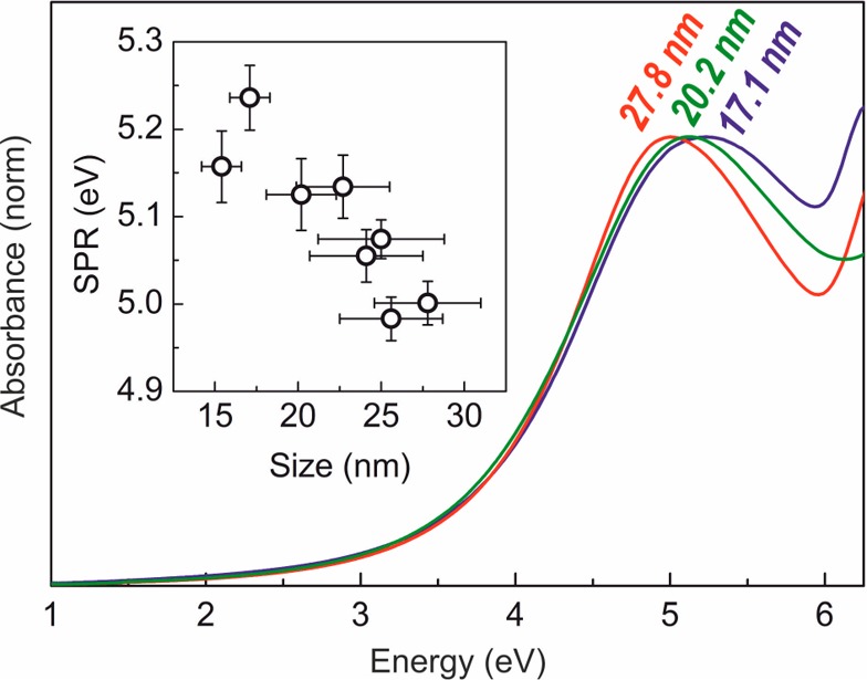
UV–vis absorption spectra of Ga NPs dispersed in hexane. Inset shows SPR values of all measured samples.
Chemical Stability
The propensity for a metal to form an oxide shell under exposure to ambient air depends on many factors and is an important consideration for the practical suitability for plasmonic applications. Despite the large enthalpy of the formation of its oxide (−1089.1 kJ/mol),28 nanoscopic Ga is by far more oxidation resistant than nanoscopic Al with an even higher enthalpy for oxidation (−1675.7 kJ/mol). Moreover, Ga is also much more stable than seminoble Ag or Cu. This can be explained by the formation of a thin and dense native oxide layer on the exterior of the Ga NPs, which is non-permeable for oxygen, chemically inert, and which is also stable on non-planar surfaces. Only the latter property seems to be absent for Al, which is sufficient to cause much higher oxygen sensitivity of nanoscopic Al. Previous studies using surface X-ray scattering29 provided that a ∼0.5 nm amorphous oxide layer is formed on the liquid Ga film upon exposure to oxygen. Oxide thickness of ∼1 nm was also estimated by X-ray photoelectron spectroscopy.30 In the present study, an oxide thickness of ∼2–3 nm on highly curved NP surface was nearly constant over extended storage under ambient conditions. Furthermore, we attempted accelerated oxidation by exposing a monolayer of Ga NPs to oxygen–argon plasma (25% O2, 75% Ar). The oxide shell thickness increased after 10 min of plasma treatment from 2 to 4 nm and stayed then nearly constant for another hour of treatment (see TEM images in Figure S20). Ga NPs remain liquid at room temperature and upon extended storage in the fridge (ca. −10 °C) for at least several months. Raman spectra (Figure S21) indicate that oxide shell remains amorphous upon storage and upon plasma treatment, as seen from the absence of β-Ga2O3 or any other known crystalline oxide. Furthermore, Ga NP cores also do not show any Raman scattering signal because of their liquid state with highly symmetric vibrations of Ga2 dimers.31
Ga NPs As Anode Material for Li-Ion Batteries
Materials forming alloys with Li, most commonly Si, Ge, Sn and Sb,32 are actively researched as alternatives to carbon-based anodes for rechargeable Li-ion batteries due to their 2–10-fold higher charge storage capacities as compared to commercial Graphite anodes (capacity of 372 mAh g–1). Upon full lithiation all high-capacity Li alloys undergo a huge increase in volume by 100–300%, making bulk/microcrystalline materials fully impractical due to fast pulverization of electrodes. Nanostructuring of the active material, by producing nanowires, NPs, and nanocrystals (NCs), has proven to be very efficient for mitigating the effects of volumetric changes and for enhancing the kinetics of the alloying reactions.33 Ga can host 2 Li atoms per Ga atom upon full lithiation, and through the formation of Li2Ga alloy delivers a high theoretical gravimetric capacity of 769 mAh g–1. Capacities of 200–400 mAh g–1 were previously obtained in LiGa alloys,34 CuGa alloys,35 and Ga droplets confined in carbon matrix.36 In this study, we examined colloidal Ga NPs as an anode material for Li-ion batteries and compared the results to bulk Ga, tested under identical conditions (Figure 8). Prior to the electrochemical measurements, insulating long-chained capping ligands were removed by treating with 1 M solution of hydrazine in acetonitrile. All electrodes were measured vs metallic lithium in half-cells and contained 64 wt % of active material, carboxymethylcellulose (CMC, 15 wt %) as a polymer binder and amorphous carbon as a conductive additive (21%). The films were casted from aqueous slurries, and after vacuum drying had similar mass loading of ∼0.5 mg/cm2. Fluoroethylenecarbonate (FEC) was used as electrolyte additive for stabilizing the solid–electrolyte interface (SEI).33b
Figure 8.
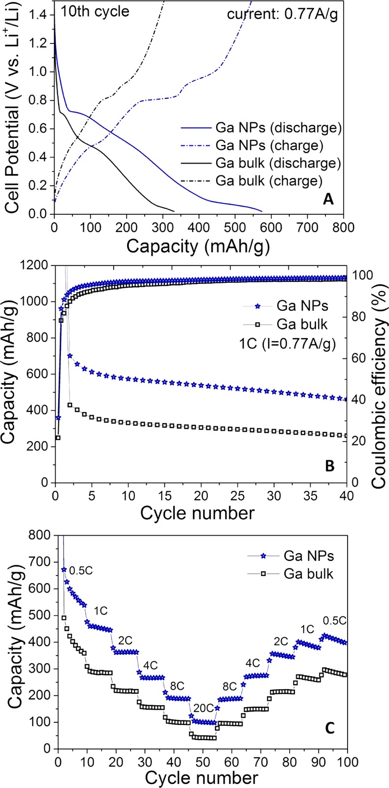
Electrochemical performance of ∼20 nm Ga NPs and of bulk Ga as anode materials for Li-ion batteries. Two-electrode half-cells with metallic Li as counter electrode were assembled. (A) Galvanostatice charge/discharge curves; (B) cycling stability tests; (C) rate-capability tests (0.5–20C rates, where 1C is a current density of 769 mA g–1 based on the theoretical capacity of pure Ga). All batteries were cycled in the voltage window of 0.02–1.5 V.
The profiles of discharge and charge curves (Figure 8A) are fully identical to those reported previously for metallic Ga34b and represent stepwise lithiation of Ga through intermediate alloys (Ga ↔ Li2Ga7 ↔ LiGa ↔ Li3Ga2 ↔ Li2Ga). Our results indicate that Ga NPs exhibit at least 50% higher reversible capacity than bulk Ga (Figure 8B), also higher than in any previous report on Ga,34a,35,36 indicating that, due to smaller diffusion path and larger electrode–electrolyte interface area, a greater fraction of Ga atoms is engaged into the reaction. Rate-capability tests are also consistent with enhanced reaction kinetics (Figure 8C). Even after reaching 20C rate, most of the capacity can recover to the initial level upon decrease of the current density to 0.5–1C. These results indicate that Ga NPs may serve as a high-energy-density anode material in Li-ion batteries. Its liquid state at ambient conditions may enable a better mitigation of the mechanic stress caused by the volumetric changes through self-healing mechanism. Hence it is of high interest to explore also the composites of Ga with other active materials.
4. Conclusions
In summary, we demonstrated the first chemical synthesis of monodisperse 12–46 nm Ga NPs using thermal decomposition of Ga alkylamides at 240–310 °C in ODE as a solvent. This colloidal approach provides an access to liquid Ga NPs which are chemically passivated with a thin native oxide shell and colloidally stabilized with long-chain organic capping ligands. Large and size-dependent supercooling effect of ΔT/Tm ≥ 0.5 has been observed and studied in details using variable-temperature XRD, TEM, specific heat, and EXAFS measurements. A large hysteresis of ∼100 K is observed between melting and crystallization phase transitions. The δ-Ga polymorph was found as the only crystalline phase that can be obtained by freezing Ga NPs. Ga NPs remain liquid at room-temperature and upon extended storage in the fridge (ca. −10 °C) for at least several months. We also found that the SPR of Ga NPs can be tuned between 4.97 and 5.24 eV. Furthermore, we tested Ga NPs as an anode material for Li-ion batteries and obtained Li-ion storage capacities of 600 mAh g–1, 50% higher than for bulk Ga under identical testing conditions and by a factor of 1.5–2 greater than in previous reports on Ga-based anodes. Chemical robustness, SPR energies in the UV region, and a broad temperature window of the liquid-state make Ga NPs an interesting material for future studies and applications in liquid-metal-based plasmonics and phase-change devices.3a,3c,4b,16,25a Liquid Ga NPs may also become uniquely suitable as low-melting point catalyst for solution–liquid–solid growth of nanowires.37
Acknowledgments
This work was financially supported by Marie Curie Co-fund (Empa Postdoc Programme), by European Union via FP7 Programme (ERC Starting Grant “NANOSOLID” with GA 306733 and Marie Curie Fellowship IIF-GA-2012-330524), by CTI Swiss Competence Centers for Energy Research (SCCER Heat and Electricity Storage), and by Swiss SNF (project number 200021_140245). Transmission electron microscopy has been carried out at the Empa Electron Microscopy Center. We thank the Swiss Light Source for providing beam time at the SuperXAS beamline. We also thank Prof. Christoph Müller and Qasim Imtiaz (ETH Zürich) for the use of their Raman microscope.
Supporting Information Available
File SI1 contains Figures S1–S21 with descriptions, Tables S1–S8. File SI2 contains sequence of electron diffraction patterns for 32.4 nm Gallium NPs upon cooling. This material is available free of charge via the Internet at http://pubs.acs.org.
The authors declare no competing financial interest.
Supplementary Material
References
- Robinson G. H. Acc. Chem. Res. 1999, 32, 773. [Google Scholar]
- Ghigna P.; Spinolo G.; Parravicini G. B.; Stella A.; Migliori A.; Kofman R. J. Am. Chem. Soc. 2007, 129, 8026. [DOI] [PubMed] [Google Scholar]
- a Wu P. C.; Khoury C. G.; Kim T.-H.; Yang Y.; Losurdo M.; Bianco G. V.; Vo-Dinh T.; Brown A. S.; Everitt H. O. J. Am. Chem. Soc. 2009, 131, 12032. [DOI] [PMC free article] [PubMed] [Google Scholar]; b Wu P. C.; Losurdo M.; Kim T.-H.; Giangregorio M.; Bruno G.; Everitt H. O.; Brown A. S. Langmuir 2008, 25, 924. [DOI] [PubMed] [Google Scholar]; c Yang Y.; Callahan J. M.; Kim T. H.; Brown A. S.; Everitt H. O. Nano Lett. 2013, 13, 2837. [DOI] [PubMed] [Google Scholar]
- a Zheludev N. Nat. Photonics 2007, 1, 551. [Google Scholar]; b Soares B.; Jonsson F.; Zheludev N. Phys. Rev. Lett. 2007, 98, 153905. [DOI] [PubMed] [Google Scholar]; c Zheludev N. I. J. Opt. A: Pure Appl. Opt. 2006, 8, S1. [Google Scholar]
- Liang W.; Hong L.; Yang H.; Fan F.; Liu Y.; Li H.; Li J.; Huang J. Y.; Chen L. Q.; Zhu T.; Zhang S. Nano Lett. 2013, 13, 5212. [DOI] [PubMed] [Google Scholar]
- a Di Cicco A. Phys. Rev. Lett. 1998, 81, 2942. [Google Scholar]; b Chen X. M.; Fei G. T.; Zheng K. J. Phys.: Condens. Matter 2009, 21, 245403. [DOI] [PubMed] [Google Scholar]
- a MacDonald K. F.; Fedotov V. A.; Pochon S.; Ross K. J.; Stevens G. C.; Zheludev N. I.; Brocklesby W. S.; Emel’yanov V. I. Appl. Phys. Lett. 2002, 80, 1643. [Google Scholar]; b Albella P.; Garcia-Cueto B.; Gonzalez F.; Moreno F.; Wu P. C.; Kim T. H.; Brown A.; Yang Y.; Everitt H. O.; Videen G. Nano Lett. 2011, 11, 3531. [DOI] [PubMed] [Google Scholar]; c Yi C.; Kim T. H.; Jiao W.; Yang Y.; Lazarides A.; Hingerl K.; Bruno G.; Brown A.; Losurdo M. Small 2012, 8, 2721. [DOI] [PubMed] [Google Scholar]
- Melendrez M. F.; Cardenas G.; Arbiol J. J. Colloid Interface Sci. 2010, 346, 279. [DOI] [PubMed] [Google Scholar]
- a Sun J.; Liu C.; Yang P. J. Am. Chem. Soc. 2011, 133, 19306. [DOI] [PubMed] [Google Scholar]; b Lauth J.; Strupeit T.; Kornowski A.; Weller H. Chem. Mater. 2013, 25, 1377. [Google Scholar]; c Kuo T.-J.; Kuo C.-L.; Kuo C.-H.; Huang M. H. J. Phys. Chem. C 2009, 113, 3625. [Google Scholar]
- Wang F. D.; Dong A. G.; Sun J. W.; Tang R.; Yu H.; Buhro W. E. Inorg. Chem. 2006, 45, 7511. [DOI] [PubMed] [Google Scholar]
- Nöth H.; Konrad P. Z. Naturforsch. 1975, 30b, 681. [Google Scholar]
- Ravel B.; Newville M. J. Synchrotron Radiat. 2005, 12, 537. [DOI] [PubMed] [Google Scholar]
- a Ahman J.; Svensson G.; Albertsson J. Acta Crystallogr. 1996, 52, 1336. [Google Scholar]; b Sharma B. D.; Donohue J. Z. Kristallogr. 1962, 117, 293. [Google Scholar]
- Yarema M.; Caputo R.; Kovalenko M. V. Nanoscale 2013, 5, 8398. [DOI] [PubMed] [Google Scholar]
- a Kravchyk K.; Protesescu L.; Bodnarchuk M. I.; Krumeich F.; Yarema M.; Walter M.; Guntlin C.; Kovalenko M. V. J. Am. Chem. Soc. 2013, 135, 4199. [DOI] [PubMed] [Google Scholar]; b Yarema M.; Pichler S.; Kriegner D.; Stangl J.; Yarema O.; Kirchschlager R.; Tollabimazraehno S.; Humer M.; Häringer D.; Kohl M.; Chen G.; Heiss W. ACS Nano 2012, 6, 4113. [DOI] [PubMed] [Google Scholar]; c Yarema M.; Kovalenko M. V.; Hesser G.; Talapin D. V.; Heiss W. J. Am. Chem. Soc. 2010, 132, 15158. [DOI] [PubMed] [Google Scholar]
- Bennett P. J.; Dhanjal S.; Petropoulos P.; Richardson D. J.; Zheludev N. I.; Emelyanov V. I. Appl. Phys. Lett. 1998, 73, 1787. [Google Scholar]
- a Bosio L. J. Chem. Phys. 1978, 68, 1221. [Google Scholar]; b Bosio L.; Defrain A.; Epelboin I. J. Phys. (Paris) 1966, 27, 61. [Google Scholar]
- Sharma B. D.; Donohue J. Z. Kristallogr. 1962, 117, 293. [Google Scholar]
- Bosio L.; Curien H.; Dupont M.; Rimsky A. Acta Crystallogr. B 1972, 28, 1974. [Google Scholar]
- a He H.; Fei G.; Cui P.; Zheng K.; Liang L.; Li Y.; De Zhang L. Phys. Rev. B 2005, 72, 073310. [Google Scholar]; b Borisov B.; Charnaya E.; Hoffmann W.; Michel D.; Shelyapin A.; Kumzerov Y. A. J. Phys.: Condens. Matter 1997, 9, 3377. [Google Scholar]; c Borisov B.; Charnaya E.; Kumzerov Y. A.; Radzhabov A.; Shelyapin A. Solid State Commun. 1994, 92, 531. [Google Scholar]; d Cicco A. D.; Fusari S.; Stizza S. Philos. Mag. B 1999, 79, 2113. [Google Scholar]; e Parravicini G. B.; Stella A.; Ghigna P.; Spinolo G.; Migliori A.; d’Acapito F.; Kofman R. Appl. Phys. Lett. 2006, 89, 033123. [Google Scholar]; f Pochon S.; MacDonald K.; Knize R.; Zheludev N. Phys. Rev. Lett. 2004, 92, 145702. [DOI] [PubMed] [Google Scholar]
- Rodriguez-Carvajal J.FullProf.2k, version3.2; Laboratoire Leon Brillouin (CEA-CNRS): Cedex, France, 2005.
- Bosio L.; Curien H.; Dupont M.; Rimsky A. Acta Crystallogr. B 1973, 29, 367. [Google Scholar]
- Rühm A.; Reichert H.; Donner W.; Dosch H.; Grütter C.; Bilgram J. Phys. Rev. B 2003, 68, 224110. [Google Scholar]
- Willets K. A.; Van Duyne R. P. Annu. Rev. Phys. Chem. 2007, 58, 267. [DOI] [PubMed] [Google Scholar]
- a Vivekchand S. R. C.; Engel C. J.; Lubin S. M.; Blaber M. G.; Zhou W.; Suh J. Y.; Schatz G. C.; Odom T. W. Nano Lett. 2012, 12, 4324. [DOI] [PubMed] [Google Scholar]; b Wu P. C.; Kim T.-H.; Brown A. S.; Losurdo M.; Bruno G.; Everitt H. O. Appl. Phys. Lett. 2007, 90, 2712508. [Google Scholar]; c Losurdo M.; Yi C.; Suvorova A.; Rubanov S.; Kim T.-H.; Giangregorio M. M.; Jiao W.; Bergmair I.; Bruno G.; Brown A. S. ACS Nano 2014, 8, 3031. [DOI] [PubMed] [Google Scholar]
- Atwater H. A.; Polman A. Nat. Mater. 2010, 9, 205. [DOI] [PubMed] [Google Scholar]
- Sanz J. M.; Ortiz D.; Alcaraz de la Osa R.; Saiz J. M.; González F.; Brown A. S.; Losurdo M.; Everitt H. O.; Moreno F. J. Phys. Chem. C 2013, 117, 19606. [Google Scholar]
- CRC Handbook of Chemistry and Physics; Taylor and Francis Group, LLC: New York, 2013. [Google Scholar]
- Regan M. J.; Tostmann H.; Pershan P. S.; Magnussen O. M.; DiMasi E.; Ocko B. M.; Deutsch M. Phys. Rev. B 1997, 55, 10786. [Google Scholar]
- Schön G. J. Electron. Spectrosc. 1973, 2, 75. [Google Scholar]
- Creighton J. A.; Withnall R. Chem. Phys. Lett. 2000, 326, 311. [Google Scholar]
- Park C.-M.; Kim J.-H.; Kim H.; Sohn H.-J. Chem. Soc. Rev. 2010, 39, 3115. [DOI] [PubMed] [Google Scholar]
- a Magasinski A.; Dixon P.; Hertzberg B.; Kvit A.; Ayala J.; Yushin G. Nat. Mater. 2010, 9, 353. [DOI] [PubMed] [Google Scholar]; b Chockla A. M.; Klavetter K. C.; Mullins C. B.; Korgel B. A. Chem. Mater. 2012, 24, 3738. [DOI] [PubMed] [Google Scholar]; c Kovalenko I.; Zdyrko B.; Magasinski A.; Hertzberg B.; Milicev Z.; Burtovyy R.; Luzinov I.; Yushin G. Science 2011, 333, 75. [DOI] [PubMed] [Google Scholar]; d Beattie S. D.; Larcher D.; Morcrette M.; Simon B.; Tarascon J. M. J. Electrochem. Soc. 2008, 155, 158. [Google Scholar]; e Chan C. K.; Peng H.; Liu G.; McIlwrath K.; Zhang X. F.; Huggins R. A.; Cui Y. Nat. Nanotechnol. 2008, 3, 31. [DOI] [PubMed] [Google Scholar]; f Mosby J. M.; Prieto A. L. J. Am. Chem. Soc. 2008, 130, 10656. [DOI] [PubMed] [Google Scholar]; g Alcántara R.; Jiménez-Mateos J. M.; Lavela P.; Tirado J. L. Electrochem. Commun. 2001, 3, 639. [Google Scholar]; h Klavetter K. C.; Wood S. M.; Lin Y.-M.; Snider J. L.; Davy N. C.; Chockla A. M.; Romanovicz D. K.; Korgel B. A.; Lee J.-W.; Heller A.; Mullins C. B. J. Power Sources 2013, 238, 123. [Google Scholar]
- a Saint J.; Morcrette M.; Larcher D.; Tarascon J. M. Solid State Ionics 2005, 176, 189. [Google Scholar]; b Wen C. J.; Huggins R. A. J. Electrochem. Soc. 1981, 128, 1636. [Google Scholar]
- Lee K. T.; Jung Y. S.; Kwon J. Y.; Kim J. H.; Oh S. M. Chem. Mater. 2007, 20, 447. [Google Scholar]
- Lee K. T.; Jung Y. S.; Kim T.; Kim C. H.; Kim J. H.; Kwon J. Y.; Oh S. M. Electrochem. Solid State 2008, 11, A21. [Google Scholar]
- Wang F.; Dong A.; Sun J.; Tang R.; Yu H.; Buhro W. E. Inorg. Chem. 2006, 45, 7511. [DOI] [PubMed] [Google Scholar]
Associated Data
This section collects any data citations, data availability statements, or supplementary materials included in this article.


