Abstract
Purpose:
Electronic portal imagers (EPIDs) with high detective quantum efficiencies (DQEs) are sought to facilitate the use of the megavoltage (MV) radiotherapy treatment beam for image guidance. Potential advantages include high quality (treatment) beam’s eye view imaging, and improved cone-beam computed tomography (CBCT) generating images with more accurate electron density maps with immunity to metal artifacts. One approach to increasing detector sensitivity is to couple a thick pixelated scintillator array to an active matrix flat panel imager (AMFPI) incorporating amorphous silicon thin film electronics. Cadmium tungstate (CWO) has many desirable scintillation properties including good light output, a high index of refraction, high optical transparency, and reasonable cost. However, due to the cleave plane inherent in its crystalline structure, the difficulty of cutting and polishing CWO has, in part, limited its study relative to other scintillators such as cesium iodide and bismuth germanate (BGO). The goal of this work was to build and test a focused large-area pixelated “strip” CWO detector.
Methods:
A 361 × 52 mm scintillator assembly that contained a total of 28 072 pixels was constructed. The assembly comprised seven subarrays, each 15 mm thick. Six of the subarrays were fabricated from CWO with a pixel pitch of 0.784 mm, while one array was constructed from BGO for comparison. Focusing was achieved by coupling the arrays to the Varian AS1000 AMFPI through a piecewise linear arc-shaped fiber optic plate. Simulation and experimental studies of modulation transfer function (MTF) and DQE were undertaken using a 6 MV beam, and comparisons were made between the performance of the pixelated strip assembly and the most common EPID configuration comprising a 1 mm-thick copper build-up plate attached to a 133 mg/cm2 gadolinium oxysulfide scintillator screen (Cu-GOS). Projection radiographs and CBCT images of phantoms were acquired. The work also introduces the use of a lightweight edge phantom to generate MTF measurements at MV energies and shows its functional equivalence to the more cumbersome slit-based method.
Results:
Measured and simulated DQE(0)’s of the pixelated CWO detector were 22% and 26%, respectively. The average measured and simulated ratios of CWO DQE(f) to Cu-GOS DQE(f) across the frequency range of 0.0–0.62 mm−1 were 23 and 29, respectively. 2D and 3D imaging studies confirmed the large dose efficiency improvement and that focus was maintained across the field of view. In the CWO CBCT images, the measured spatial resolution was 7 lp/cm. The contrast-to-noise ratio was dramatically improved reflecting a 22 × sensitivity increase relative to Cu-GOS. The CWO scintillator material showed significantly higher stability and light yield than the BGO material.
Conclusions:
An efficient piecewise-focused pixelated strip scintillator for MV imaging is described that offers more than a 20-fold dose efficiency improvement over Cu-GOS.
Keywords: electronic portal imaging device (EPID), megavoltage (MV) imaging, piecewise focusing, high detective quantum efficiency (DQE), cone-beam computed tomography (CBCT), cadmium tungstate (CWO)
1. INTRODUCTION
The low detective quantum efficiencies (DQEs) of electronic portal imagers (EPIDs) have limited their use for image-guided radiotherapy (IGRT) particularly when good soft tissue contrast resolution is required. Previous studies have shown that a DQE(0) of 20% is desired to achieve acceptable image quality at acceptably low doses.1–5 If such a level of performance could be attained, some unique advantages may be conferred. These include high quality beam’s eye view imaging for intrafraction motion management, and metal artifact-free cone-beam computed tomography (CBCT) reconstructions of more accurate electron density for improved patient setup and treatment replanning.1,3,6–8 CBCT acquisition speeds and/or image quality also could be increased by combining kV with high quality megavoltage (MV) data.9,10
Most EPIDs use an indirect detection mechanism.14,15 A 1 mm-thick copper build-up plate is coupled to a thin terbium-doped gadolinium oxysulfide scintillator screen (Cu-GOS) that, in turn, is mounted on to an active matrix flat panel imager (AMFPI) incorporating amorphous silicon thin film electronics. The Cu-GOS assembly converts the incoming x-ray photons into optical photons which are then detected by the AMFPI. Because of the high amounts of optical scattering in the GOS layer, it is preferred that the GOS area density be kept below 400 mg/cm2 thus limiting the imager’s DQE(0) to approximately 1%.16–19 A promising means of increasing EPID sensitivity is to replace the Cu-GOS assembly with an array of thick pixelated scintillators.4,5,20,21 Key properties of several candidate scintillator materials are shown in Table I.
TABLE I.
Properties of common scintillators. Adapted from Refs. 11–13.
| Scintillator | Density (g/cm3) | Index of refraction | Light yield (photons/MeV) | Output stability and radiation hardness | Cleave plane | Optical transparency | Hygroscopic |
|---|---|---|---|---|---|---|---|
| Bi4Ge3O12 (BGO) | 7.2 | 2.2 | 8 000 | Low | No | High | No |
| CdWO4 (CWO) | 7.9 | 2.3 | 15 000 | High | Yes | High | No |
| CsI:Tl (CsI) | 4.5 | 1.8 | 65 000 | Moderate | No | High | Yes |
| Gd2O2 S:Tb (GOS) | 7.3 | 2.3 | 60 000 | High | No | Low | No |
The first large-area, high sensitivity portal imager was built by Seppi et al.20 A 9 mm-thick, 40 × 30 cm wide, thallium-doped cesium iodide (CsI) pixelated scintillator was coupled to an AMFPI. Results showed that sensitivity was significantly increased relative to that obtained with a conventional Cu-GOS screen, and CBCT scans taken with the imager were shown to be useful for monitoring interfractional lung tumor changes.7 However, the DQE(0) at 6 MV was still less than 10% and, as a result, the imager was not deemed to be suitable for general purpose image guidance.2 Moreover, despite the small pixel size of 0.396 mm, spatial resolution was only about half that provided by the Cu-GOS screen due to light sharing between pixels. Resolution was further reduced toward the imager’s periphery due to parallax since the array was not focused toward the source.
Sawant et al.21 built a 16 × 16 cm2 pixelated CsI imager that was 40 mm thick and had a pitch of 1 mm. DQE(0) at 6 MV was measured to be 22%. In comparisons with a Cu-GOS screen, significant improvements in radiographic image quality were shown. However, as with the Seppi imager, spatial resolution was degraded by optical cross talk and by the lack of focusing. Using 120 × 60 pixel imagers, Wang et al.22 and El-Mohri et al.23 showed that bismuth germanate (BGO) may be a preferred scintillator due to its higher density and higher index of refraction. For a given quantum efficiency, the increase in density allows the pixel height to be reduced thus reducing beam divergence effects, and the higher index of refraction increases the probability that optical photons undergo total internal reflection at the pixel-glue boundaries thus reducing cross talk. Disadvantages of BGO are its low light output and lack of radiation hardness. Preirradiation of the scintillator with 2000 cGy was required to achieve acceptable output stability for the projection imaging and CBCT studies that were reported.
An alternative scintillator is sintered GOS which is commonly used in diagnostic CT detectors.11 While suitable for lower energy systems, the low optical transmissivity of the ceramic material may contraindicate its use for constructing pixels with high aspect ratios as is required for high energy applications. Breitbach et al.24 studied ceramic GOS for imaging at 6 MV using a pixelated array of area 40 × 10 cm and thickness of 1.8 mm. A modest 2.5 × sensitivity increase was achieved when compared to Cu-GOS performance.
Cadmium tungstate (CWO) shares many of the advantages of BGO and ceramic GOS including a high density (7.9 gm/cm3) and high index of refraction (n = 2.3), but with fewer liabilities. Compared to BGO, CWO has a high radiation resistivity (107 rad) and has twice the light output. Compared to sintered GOS, CWO is highly transparent. The main challenge of working with CWO results from the cleave plane inherent in its crystal structure, which makes the material difficult to machine and polish for purposes of constructing pixels with high aspect ratios.
Rathee et al.4 built a piecewise-focused 1D CWO scintillator array with a 2.75 mm transaxial pitch and 10 mm thickness. Custom electronics arrayed in a piecewise-focused arc were developed for readout and digitization. A DQE(0) of 19% at 6 MV was measured and the spatial resolution of the CT reconstruction at the isocenter was 5 lp/mm. This study was followed up by Kirvan et al.25 who built an arc detector consisting of 20 two-dimensional arrays, each with 16 × 16 pixels with 1 mm pitch. The total imaging area comprised 5100 pixels and measured 16 × 320 mm. Custom photodiodes and electronics were used for readout and CBCT scans were acquired by rotating the phantom. In general, the use of readout and digitization electronics that are separate from an (radiation hard) EPID risks making the approach less practical for commercialization with a flat panel imager.
The goal of this work was to construct a larger area AMFPI-based “strip” detector from CWO pixels which can be suitable for clinical testing.26 At 6 MV, a DQE(0) value greater than 20% was targeted along with a CBCT spatial resolution of 7 lp/cm across the entire field-of-view (FOV) to match that of commercial kV-based systems used for IGRT.27,28 As described below, focusing was achieved by coupling pixelated scintillator subarrays to a Varian AS1000 EPID (Varian Medical Systems, Palo Alto, CA) through a piecewise arc-shaped fiber optic plate (FOP).
2. METHODS AND MATERIALS
2.A. Scintillator subarrays
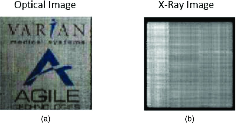
A total of seven subarrays, each 15 mm thick and having an area of 51.7 × 51.7 mm, were fabricated. Six of the subarrays were constructed from CWO, and one from BGO. The CWO subarrays each contained 66 × 66 square pixels with a pitch of 0.784 mm while the BGO subarray had a larger pitch of 1.17 mm to compensate its lower light output. These pitches were integer multiples of the intrinsic AS1000 AMFPI pixel pitch of 0.392 mm. Figure 1 shows example optical and x-ray images of a CWO subarray. High optical transparency is demonstrated. In total, the seven arrays contained 28 072 pixels.
FIG. 1.
(a) Optical image showing the high transparency of a 66 × 66 pixel CWO subarray. The logos are situated behind the backlit subarray. (b) Flood-field x-ray image obtained using a 6 MV source and a modified AS1000 EPID as the receptor (not gain corrected). There are 2 × 2 EPID pixels per scintillator pixel.
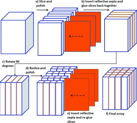
The subarrays were fabricated by Agile Technologies (Knoxville, TN) using the slicing and gluing technique described by Uribe et al.29 and illustrated in Fig. 2. Briefly, a block of scintillator is cut into slabs and both sides of each slab are polished. A reflector is then inserted between the slabs which are glued back together to reform the block. The same cutting, polishing, and gluing processes are then repeated in the orthogonal direction. After construction, the lateral sides of each subarray were beveled at a 1° angle to enable close packing onto the FOP (see Fig. 3), and the tops of each subarray were covered with Vikuiti ESR specular reflector film (3M Corp, Minnesota).
FIG. 2.
Scintillator array fabrication technique employing slicing and regluing operations. 2(N − 1) cuts and 4(N − 1) polishing and gluing steps are required to construct an array comprising N2 pixels.
FIG. 3.
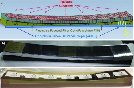
Piecewise-focused strip assembly. The total area covered is 361 × 52 mm and comprises 28 072 scintillator pixels. (a) Schematic showing pixelated subarrays mounted to a custom FOP comprising seven sections (W0, W1a,b, W2a,b, W3a,b) which, in turn, are coupled to the AMFPI. (b) Photograph of the scintillator-FOP structure after partial assembly. The BGO subarray is in position W3b with its top covered by a reflector. The other subarrays have not yet been covered. (c) The scintillator-FOP structure after final assembly.
2.B. Scintillator strip assembly
The seven subarrays were coupled to a piecewise-focused FOP as shown in Fig. 3. The total area of coverage was 362 × 52 mm. The custom FOP was manufactured by Incom, Inc. (Charlton, MA) from the BXE387 fiber material with a core diameter of 6 μm, and consisted of seven sections bonded together, each with a top surface area of 51.7 × 51.7 mm to match that of the subarrays. The top surface of the central section (W0) of the FOP was parallel to the AMFPI, while the other sections of the FOP were wedge-shaped with their centers pointing to the source located a distance of 150 cm normal to the center of W0. The first set of FOP wedges (W1a and W1b), glued to the left and right sides of W0, respectively, had a top surface angle of 2°. The next pair (W2a and W2b) had a top surface angle of 4°, and third pair (W3a and W3b) had a top surface angle of 6°. Hence, the maximum divergence angle across the entire FOV was only 1° and occurred at the four edges of each subarray. The height of the central FOP section was 5 mm and increased to 16 mm at the lateral edges of W3a and W3b. The optical fibers were aligned normal to the top surface. The scintillator arrays were bonded to the FOP using MeltMount glue (Cargille Labs, Cedar Grove, NJ) and the top and sides of the assembly were wrapped in an opaque tape. The entire scintillator-FOP assembly was mechanically coupled to the AMFPI using a custom aluminum fixture with a carbon fiber top. Figure 3(a) illustrates the configuration and Fig. 3(c) contains a photograph of the completed assembly.
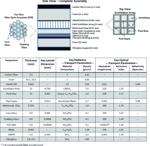
The cross section of entire detector is shown in Fig. 4, and comprised, from top to bottom: a top cover, foam spacer, top reflector, pixelated scintillator array, glue layer, fiber optic plate, Mylar protective sheet, AMFPI, and backing layers. The scintillator pixel width was 0.758 mm, glue (epoxy) thickness was 0.007 mm, and reflector thickness was 0.013 mm resulting in a pixel pitch of 0.784 mm and fill factor of 93%. The top (Vikuiti ESR) and side (aluminum-coated mylar) reflectors surrounding each scintillator pixel were specular with a reflectivity profile verified using the measuring device previously described by Janecek and Moses.30 All optical transport parameters are given in the table below Fig. 4. The AMFPI pixel size was 0.392 mm.
FIG. 4.
Top: schematic of the detector assembly including a cross section of the FOP (top left) and the scintillator array (top right). Bottom: table of radiative and optical transport parameters used in the simulations. Optical transport parameters were provided by manufacturers with the key transport parameters describing the Vikuiti ESR reflector and aluminized Mylar septa confirmed experimentally.
2.C. Monte Carlo simulations
Monte Carlo simulations of radiative and optical transport were conducted to predict the performance of the detector and to optimize its design. The DQE, modulation transfer function (MTF), and the noise power spectrum (NPS) were determined using the recently developed Fujita-Lubberts-Swank (FLS) algorithm31 illustrated in Fig. 5 and summarized below.
FIG. 5.
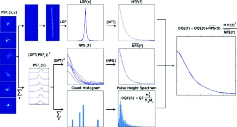
Schematic flow chart of the FLS simulation method. [Reprinted from Star-Lack et al. “Rapid Monte Carlo simulation of detector DQE(f),” Med. Phys. 41(3), 031916 (18pp.) (2014). Copyright 2014, American Association of Physicists in Medicine (AAPM).] Each gamma photon that interacts with the imager produces a typically unique 2D point-spread function. To compute the NPS, each PSF is summed along 1D to yield a PSF projection which is Fourier transformed and squared to generate a NPS (Ref. 32). The NP spectra from all events are summed and normalized to compute the NPS shape (middle row). Each PSF is also individually summed to give the total received counts for that event, which is then tallied into a pulse height spectrum from which the DQE(0) is calculated using the Swank formalism (Ref. 33) (bottom row). By directing the gammas along an angled line, the MTF can be determined following the Fujita procedure (Ref. 34) (top row). The results of these calculations are then combined to yield the final DQE(f) (right).
The frequency-dependent DQE is computed as follows:
| (1) |
where q is the input x-ray photon (gamma) fluence in units of gammas/mm2 and NNPS(f) is the frequency-dependent normalized noise power spectrum.
For the FLS simulation, Nγ gamma photons are directed toward the detector along an angled line and the PSF for each event is recorded. The shape of the 1D NPS produced by each detected gamma photon p along (in this case) the x-axis is computed by summing the PSF in the y-direction and taking the square magnitude of its Fourier transform
| (2) |
Here, i, j label detector pixels along the x, y directions, respectively, and the DFT operator refers to the 1D discrete Fourier transform taken, in this case, in the i-direction. According to the Lubberts relation,32 the shape of the resulting NPS curve, up to a scale factor, is obtained by averaging NPSp(f) over all detected events Np,
| (3) |
To generate the NPS scaling factor, we note that product of q and the zero-frequency NNPS [NNPS(0)] is the reciprocal of the zero-frequency DQE [DQE(0)], which can be determined from the measured quantum efficiency (QE = Np/Nγ) and the pulse height spectrum using the Swank formula33 to account for the effects of the x-ray spectrum and the energy-specific detector response on SNR,
| (4) |
where Mk label kth moment of the pulse height spectrum. Hence, the denominator of the DQE(f) expression [Eq. (1)] is the normalized NPS shape as determined by Eq. (3) divided by DQE(0) from Eq. (4),
| (5) |
The numerator of Eq. (1) [i.e., MTF2(f)] is readily computed from the oversampled line-spread function (LSF).34
The FLS simulation method was implemented using custom geant4 (Ref. 35) Monte Carlo code, which has the unique capability of modeling both radiative and optical photon transports. For radiative transport, the penelope Low Energy Physics package was invoked with a range cut of 0.5 μm to maximize accuracy.
The FOP was modeled using the core and cladding glass transport parameters contained in the table in Fig. 4. Due to geometric constraints in the simulation software package, the statistical extramural absorption (EMA) configuration used to prevent light spread (1 black fiber for every 20 clear fibers) was modeled using a circumferential arrangement to give equivalent results as determined from an analytical model. This was achieved by surrounding each fiber with 0.08 μm-thick partially attenuating outside layer having an absorption length of 0.23 μm. In experiments, we saw no resolution loss due to the FOP.
The x-ray beam spectrum was generated following the methodology of Constantin et al.36 The source model included a 6 MV electron beam impinging on a tungsten target and producing x-rays through a bremsstrahlung process. The forward-directed x-rays were attenuated by a tungsten flattening filter and interacted with relevant hardware including the “jaw” collimators which were set to produce a 10 × 10 cm field located at a distance of 100 cm from the source.
For each FLS simulation, 5000 gamma photons were sampled from the 6 MV spectrum and launched. The optical yield was set to 600 photons/MeV to minimize run times while still preserving accuracy.31 The average simulation time per run, using a Dell Latitude E6400 laptop computer (Dell Inc, Austin, TX) with an Intel Core i7 processor (Intel Inc, Santa Clara, CA), was 95 CPU-minutes.
2.D. Experimental studies
Measurements were performed at the Georgia Tech Radiation Science and Engineering Laboratory using a Varian C-series Trilogy System (Palo Alto, CA). The 6 MV beam was used with the flattening filter in place, and all studies were conducted in gated fluoroscopy mode with the “beam-on” and “imager exposure” periods coincident so that no dose was wasted and exposure from frame-to-frame was constant. Measurements of MTF, NPS, and DQE were made, and 2D and 3D imaging studies were conducted.
2.D.1. Single subarrays
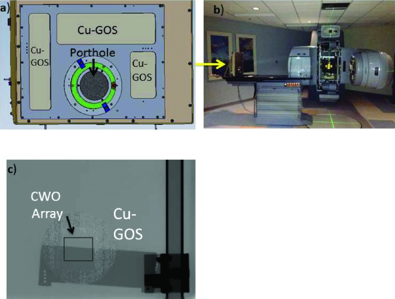
Before constructing the entire strip assembly, the performance of individual scintillator subarrays coupled to test FOP pieces was assessed using a modified AS1000 EPID containing a “porthole” to provide ready access to the amorphous silicon readout array [Fig. 6(a)]. A 51.7 × 51.7 mm2 scintillator subarray was coupled to an equivalent sized FOP and pressed onto the amorphous silicon sensor so that the resulting stack matched that shown in Fig. 4 but without the Meltmount glue layer. For comparison with existing technology, the portion of the imager outside the porthole was covered with a 1 mm copper build-up plate attached to 133 mg/cm2 of GOS. The modified imager was placed upright on the patient couch directly across from the source which was rotated to a 90° position as shown in Fig. 6(b). The source-to-imager distance (SID) was 320 cm and the collimation “jaws” were set such that the entire 40 × 30 cm imager was irradiated. To measure the effects of beam divergence, the imager was shifted laterally from the center of the radiation field, thus shifting the porthole a distance d from the center of the radiation field to create a divergence angle α given by α = arctan(d/320).
FIG. 6.
Experimental setup for measuring MTF, NPS, and DQE. (a) Modified porthole imager allowing for individual subarrays and FOP sections to be tested for comparison to the conventional Cu-GOS scintillator. (b) The Linac is rotated 90° and the imager is attached to the patient table for measurements. (c) Typical edge image. The edge phantom spans both the porthole (CWO array) and a Cu-GOS section.
Measurements of MTF and NPS were made at for α = 0°, 1°, and 6° using either the W0 (central) FOP segment or the W3 (outer) FOP segment. As the validity of frequency domain analysis depends on stationarity, we note that the CWO-W0 FOP subassembly is spatially invariant since the pixel size of the CWO subarrays (0.784 mm) is exactly twice the a-silicon detector pixel size (0.392 mm). The CWO subarrays were constructed with very high precision so that pixel-to-pixel pitches varied by at most only ±0.025 mm with a total accumulated error of only 0.08 mm over a subarray, and the a-silicon pixels are highly regular since they are lithographically etched. The other pixelated element in the stack is the FOP which is not strictly wide-sense stationary (WSS) but has such small irregularities that any errors in periodicity (<0.01 μm) are insignificant when compared to the a-silicon pitch of 0.392 mm. The CWO-W3 FOP subassembly in the vertical direction is also WSS but, in the horizontal direction, is cyclostationary because the size of the CWO pixel projected onto the a-silicon detector is 1.99 × (not exactly 2 ×) the size of the a-silicon pixel due to the 6° angle of FOP wedge. Nevertheless, frequency domain measurements are still justified.37
The MTF was computed using an edge-spread function (ESF) measurement which has not traditionally been applied at MV energies but is equally applicable as shown in the Appendix. Briefly, a 0.5 mm thick tantalum sheet was angled at 2.5° and placed 10 cm in front of the imager to minimize the effects of forward scatter on MTF. Given the large SID of 320 cm, the effect of focal spot blurring on the MTF measurement was negligible (less than 0.05 mm assuming a 1.5 mm focal spot size). For each CWO measurement, 512 frames of flood-field and edge-field data were acquired at a tube output of 1 monitor unit (MU)/frame resulting in a cumulative detector dose of 50 cGy per image (each Cu-GOS MTF measurement was with twice the dose). Note, the system was calibrated so that 1 MU yields a dose of 1 cGy at a distance 100 cm from the source at a depth dMax = 1.5 cm of water. Hence, we assume a detector exposure equal to 1 cGy/MU multiplied by the geometric factor (100/SID)2. After normalization, the ESF, LSF, and MTF were calculated using conventional means employing 4 × oversampling and Savitzky-Golay differentiation where correction was made for the low pass effects of differentiation operation.38 Figure 6(c) shows a normalized image taken of the tantalum plate spanning a portion of the imager covered by the CWO array (porthole) and a portion covered by the Cu-GOS layer.
The quantity qNNPS, which is the denominator of the DQE formula [Eq. (1)], was measured by acquiring 512 sequential images at a detector exposure of 0.098 cGy/frame at a rate of 5 frames/s (fps). For each CWO dataset, the central 80 × 80 AMFPI pixels of the porthole were processed according to the conventional IEC method,39,40 whereby a 2D qNNPS is first computed and transformed into a 1D qNNPS by averaging the first ten rows on either side of, but not including, the zero-frequency axis. A KERMA dose equivalent factor of 1.42 × 10⁷ photons/(cGy − mm2) was used to convert exposure to input fluence.31 For the Cu-GOS NPS calculations, 80 × 80 AMFPI pixels were processed from the region just above the porthole. The DQE(f) was determined using Eq. (1) by dividing the quantity MTF2(f) by qNNPS(f).
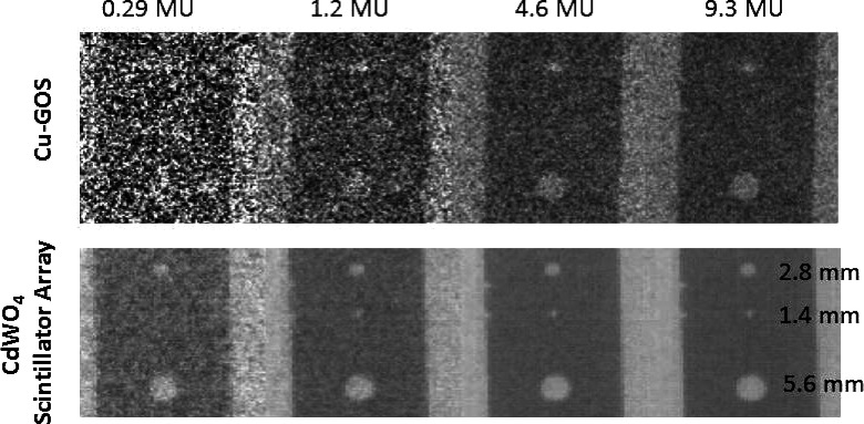
Using the porthole imager, projection images were taken of a hole-type image quality indicator “5.5 aluminum penetrometer” per ASTM E0125-11 standards (American Society of Testing and Materials, 2011). The penetrometer was 1.397 mm-thick (0.055 in.) and contained three holes with the following diameters—1 T (1.397 mm), 2 T (2.794 mm), and 4 T (5.588 mm). To approximate clinical conditions, 30 cm of solid water was placed between the penetrometer and imager. Images were acquired at effective outputs of 0.29, 1.2, 4.6, and 9.3 MU which are defined as the tube outputs that would yield the equivalent SNR had the detector been positioned in its conventional position 150 cm from the source, and is given by the actual MU multiplied by the ratio of (150/320)2. Gain correction was performed by dividing the raw data sets by a high SNR flood-field data set.
2.D.2. Strip assembly
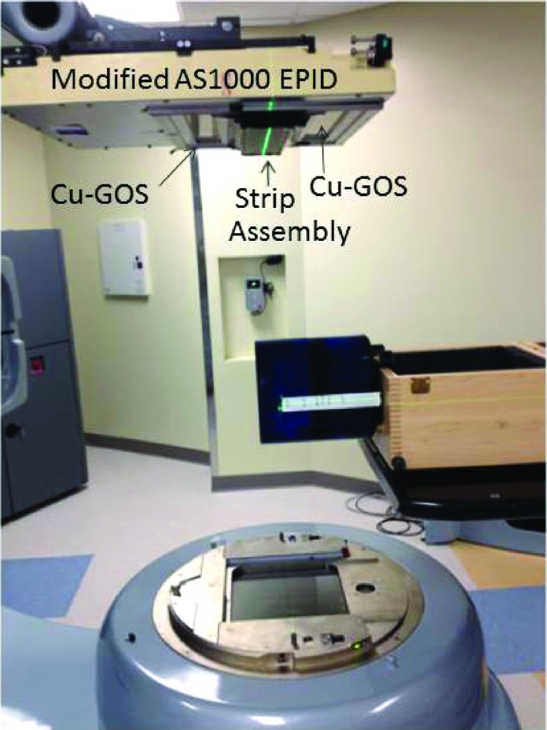
The entire strip assembly was incorporated into an AS1000 using a custom aluminum fixture with a carbon fiber top. Figure 7 shows a photograph of the modified EPID mounted to the Clinac. The strip assembly, which covers the central portion of the imager, is visible. The portion of the EPID not coupled to the strip was covered with Cu-GOS. The SID was 150 cm.
FIG. 7.
Modified AS1000EPID mounted to a Varian Trilogy Clinac. The top cover of the strip assembly, which traverses the entire width of the imager, is visible. In the surrounding portions, the EPID is coupled to a Cu-GOS scintillator. The CatPhan phantom, hanging off the front edge of the patient able, is also visible.
Imaging tests were conducted to assess the stability and noise properties of the strip assembly for comparison to Cu-GOS. The imager was preirradiated with approximately 100 cGy, and 20 flood-field images were acquired at 0.33 MU/frame (0.15 cGy detector exposure/frame) at a rate of 5 frames/s. These images were averaged to create a first reference image FF1 with 2.9 cGy total detector exposure. The imager was then exposed to 46 cGy, and another 20 frames were collected and averaged to create a second image FF2. The time between acquisition of FF1 and FF2 was 6 min.
A normalized difference image NDiff was computed as follows:
| (6) |
The mean of NDiff is indicative of the signal drift, and its standard deviation is indicative of the reciprocal of the SNR.
CBCT studies of the CatPhan600 (Phantom Laboratories, Salem, NY) were also conducted. Data were acquired with a gantry rotation rate of 1 RPM and a frame rate of 5 frames/s. The output per frame was 0.033 MU, with the jaws adjusted to irradiate a 7 × 40 cm FOV at the detector. By translating the imager longitudinally, data were collected using either the Cu-GOS scintillator or the CWO strip, and multiple sections of the CatPhan were scanned by longitudinally translating the patient table in a step-and-shoot mode. For each data set, 163 projections covering an angle of 210° were acquired using a total of 5.4 MU resulting in a dose of approximately 4 cGy at the phantom center (at a depth of 10 cm, the dose calibration is 0.75 cGy/MU at the system isocenter).
Reconstruction was performed using the Varian cone-beam software package (Varian Medical Systems, Palo Alto, CA), which is a toolkit comprising a suite of Windows-based software libraries enabling users to preprocess CBCT projection data with scatter and beam hardening corrections41,42 and then perform 3D reconstruction. For the strip scintillator projections, interpolation was first performed at the boundaries of each subarray to remove discontinuities. For all data sets, after the scatter and beam hardening corrections were applied, the corrected projections were fed into the FDK algorithm43 employing antialiasing filtering44 and Parker weighting45 to reconstruct 3D images with a transaxial pixel size of 0.5 mm and slice thickness of 2.0 mm. For all reconstructions, the Varian Sharp kernel was used where, for a 0.5 mm pixel, the 10% MTF roll-off point occurs at 9.9 cm−1. After reconstruction and Hounsfield unit (HU) scaling, a variable intensity ring correction algorithm was applied.46
3. RESULTS
3.A. MTF and DQE
Figure 8 shows measured and simulated MTFs and DQEs for a nondivergent beam in both the vertical (axial) and horizontal (transaxial) directions. The CWO data are from an array that, in the final assembly, was placed in position W2a (Fig. 3) and exhibited average performance. The measured and simulated CWO DQE(0) values are 22% and 26%, respectively. Note that the simulated and measured DQE(f)’s match very well in the horizontal direction while the measured vertical DQE(f) is depressed somewhat, which may point to weaknesses in the array fabrication process. Optical cross talk may be the culprit since, after the second set of cutting and regluing operations (see Fig. 2), there remains a 7 μm glue layer that could allow for some cross talk in the direction of the first cut. This will be studied in future investigations.
FIG. 8.

Simulated and measured MTFs (a) and DQEs (b) for a nondivergent beam in both the horizontal (transaxial) and vertical (axial) directions. (c) Simulated and measured DQE improvements across the frequency range of 0–0.62 mm−1. The average measured and simulated DQE improvements provided by the CWO array are 23 × and 29 ×, respectively.
Figure 8(c) shows the ratio of the mean of the vertical and horizontal CWO DQEs to the mean Cu-GOS DQE for all spatial frequencies up to the CWO Nyquist limit of 6.2 mm−1. On average, the CWO DQE(f) is 23 × and 29 × (measured and simulated) higher than the Cu-GOS DQE(f) with the maximum measured improvement of 27 × occurring at 0.22 mm−1. Although the simulation predicts the shape of the curve in Fig. 8(c) very well, there remains 25% scaling error. This is in part due to the reduced vertical DQE(f) discussed above and in part due to the simulator underestimating the DQE(f) of Cu-GOS. Note that while the CWO MTF is slightly decreased relative to the Cu-GOS MTF [Fig. 8(a)], the perceived CWO spatial resolution in the imaging studies is still significantly higher due to the increased sensitivity of the CWO array (see Figs. 11 and 14).
FIG. 11.
Projection images of aluminum penetrometer acquired at 0.29, 1.2, 4.6, and 9.3 MU. The measured contrast is 0.9%. The CWO array is shown to provide a 27 × dose efficiency improvement.
FIG. 14.
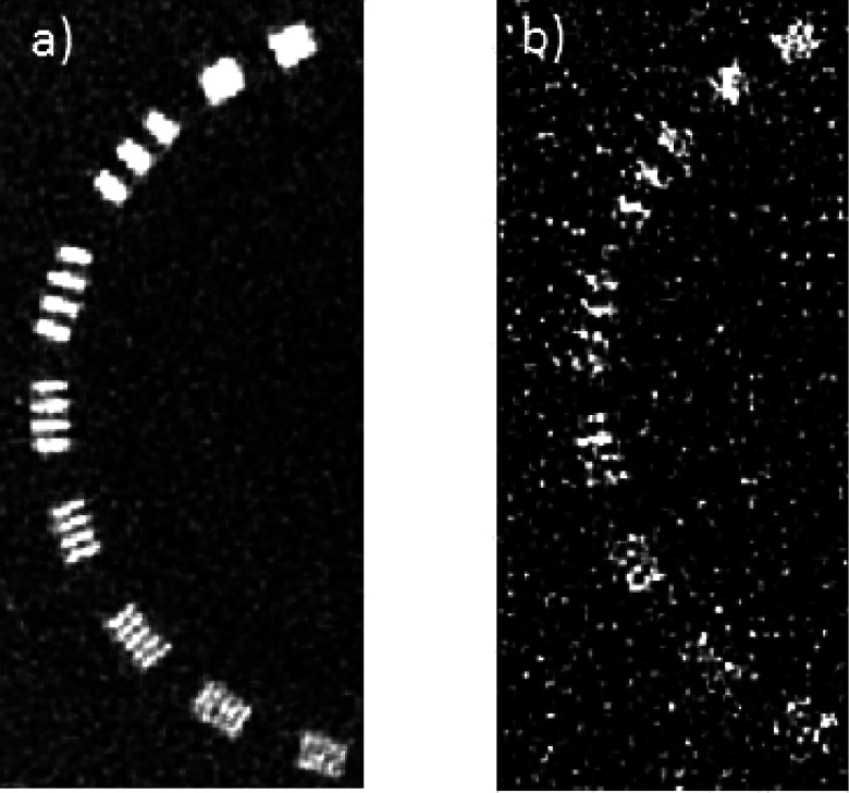
Reconstructions of the high contrast spatial resolution CatPhan module (window width = 600 HU). (a) CWO image—7 lp/cm spatial resolution is realized. (b) Cu-GOS image—because of the low CNR, spatial resolution is difficult to assess. Data were acquired with 5.4 MU producing a dose of 4 cGy at the phantom center.
Figure 9 shows the advantages of focusing the scintillator to the source. For a 6° divergence angle, corresponding to the central positions of the W3a,b FOP pieces in the strip assembly, the unfocused MTF is severely decreased [Fig. 9(a)] which results in more than a 5 × DQE loss for spatial frequencies greater than 4 mm−1 [Figs. 9(b) and 9(c)]. On average, the unfocused detector suffers DQE losses of 55% and 59% (measured and simulated) across the entire frequency range. The piecewise-focused design reduces the maximum divergence angle across the FOV to 1°. As shown in Fig. 10, a 1° divergence angle has minimal impact on performance as the average measured and simulated DQE losses are only 4% and 6%, respectively.
FIG. 9.

Measured and simulated CWO MTFs and DQEs for 6° beam angle (W3b position in Fig. 3). Results are shown for both a focused and unfocused beam in the horizontal (transaxial) direction where the effects of focusing are observed. The unfocused array suffers a significant MTF loss (a) causing a large reduction in DQE (b). (c) The ratio of the unfocused to focused DQE across the frequency range of 0–0.62 mm−1. The average measured and simulated losses incurred by a lack of focusing are 55% and 59%, respectively.
FIG. 10.

Negligible degradation of MTF and DQE occurs for a 1° divergence angle, which is the worst case encountered using proposed piecewise-focused design. (a) MTF curves, (b) DQE curves, and (c) ratio of 1°/0° DQE values as a function of spatial frequency. The average measured and simulated DQE losses are 4% and 6%, respectively.
3.B. Imaging studies
Results from the penetrometer studies are shown in Fig. 11. A dramatic improvement in detectability and contrast-to-noise ratio (CNR) is provided by the CWO array as all three holes, each with a contrast of 0.9%, are visualized with a dose of 1.2 MU. In comparison, the 1.4 mm hole cannot be visualized in any of the Cu-GOS images (the maximum dose tested was 9.3 MU). At the lowest dose of 0.29 MU, the 2.8 and 5.6 mm holes are detected in the CWO images, while no holes are visualized in the Cu-GOS image. Assessment of relative CNR2 shows that CWO array dose efficiency is 27 × Cu-GOS dose efficiency, which is consistent with DQE results reported above.
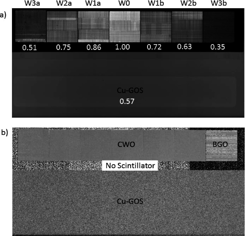
Figure 12(a) shows a portion of the raw data flood-field image FF1 that includes the 36.4 × 5.2 cm scintillator strip and the lower Cu-GOS region. The assembly was fabricated so that the brightest pieces were positioned in the middle of the row where x-ray attenuation generally is the highest (the relative average intensity of each subarray is shown beneath each subarray). There are several reasons for the variations in intensity. The CWO subarray W3a, which has the lowest intensity of all the CWO subarrays, was the first one manufactured and the polishing and cutting processes were beginning to be optimized. W3b is the BGO array with, on average, 2.5 × lower intensity than that of the CWO subarrays, which is consistent with published figures for relative scintillator yield (see Table I). The four CWO subarrays W2a,b and W1a,b have similar intensities, which range between 63% and 86% of the intensity of the W0 subarray, which was the last subarray manufactured and the best polished. Note that variations in FOP thicknesses due to the piecewise arc shape were not found to be the cause of the CWO signal intensity variations as it was observed by measurement and simulation that the FOP reduces the signal intensity by approximately 50% for all sections. Note also that, due to its lower quantum efficiency, Cu-GOS intensity is below CWO intensity despite the higher intrinsic scintillation yield of GOS.
FIG. 12.
(a) Raw data flood-field image (FF1) showing the scintillator strip (not gain corrected) and the GOS region. The relative signal intensities of each of the subarrays are shown below each subarray. (b) Normalized noise image NDiff computed using Eq. (6). The window width is 1.5%. Increased stochastic noise is seen in the Cu-GOS region, and increased patterned noise is seen in the BGO subarray. The measured CWO sensitivity is 22.5 × Cu-GOS sensitivity based on SNR measurements (see Table II).
Figure 12(b) shows the normalized noise image NDiff computed from FF1 and FF2 [Eq. (6)]. There is minimal structured noise in the Cu-GOS and CWO regions while the BGO array exhibits horizontal banding indicating that the scintillation yield may have drifted in a spatially nonuniform manner between the times that the two images were acquired. As expected, stochastic random noise is the highest in the Cu-GOS region. A ROI was drawn on each CWO subarray (the boundaries were excluded) and the mean error and standard deviation of the noise were computed. Seven corresponding ROIs were drawn on the Cu-GOS scintillator region below the strip and the same computations were made. Results are contained in Table II, which shows that the mean drift of the BGO signal is 10 × the mean CWO drift which appears to be the lowest of the three scintillators. The relative CWO dose efficiency (equal to relative SNR2) is 22.5 × Cu-GOS dose efficiency. Due to structured noise, the apparent dose efficiency of the BGO array is only slightly above that of Cu-GOS.
TABLE II.
Mean drift, relative SNR, and relative dose efficiency of Cu-GOS, BGO, and CWO as determined from the means and standard deviations of ROIs taken in the noise image, NDiff [see Eq. (6)].
| Scintillator | Mean drift (%) | Relative SNR | Relative dose efficiency (sensitivity) |
|---|---|---|---|
| Cu-GOS | 0.063 | 1 | 1 |
| BGO | 0.238 | 1.28 | 1.64 |
| CWO | 0.0025 | 4.74 | 22.5 |
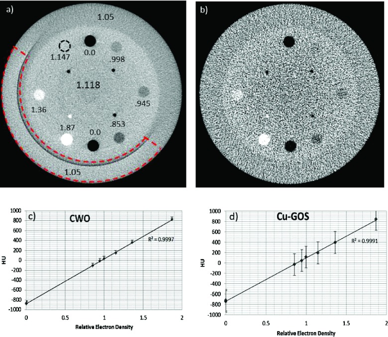
Figure 13 shows CBCT reconstructions of the CTP404 module of the Catphan600 which measures contrast resolution and HU vs electron density response. The module has eight inserts with the following relative (to water) electron densities: air—0.0, polymethylpentene (PMP)—0.853, low density polyethylene (LDPE)—0.945, polystyrene—0.998, acrylic—1.147, Delrin—1.363, and Teflon—1.868. The background relative electron density is 1.118, and the relative density of the outer annulus is 1.05. In the CWO image [Fig. 13(a)], all inserts can be seen except for acrylic which has 2.5% contrast relative to the background. In the Cu-GOS image 13(b), neither the acrylic insert nor the polystyrene insert with 12% contrast relative to background is visualized.
FIG. 13.
The CWO strip array provides a 22 × sensitivity improvement over Cu-GOS in CBCT reconstructions of the CTP404 Catphan module. (a) CWO image. The relative electron densities of the inserts are labeled. The area outlined with the dashed arc is subtended by the BGO array in the 210° scan and exhibits a 4% reconstruction error as evidenced by the brightness increase. (b) Cu-GOS image. (c) and (d) Both the Cu-GOS and CWO images exhibit excellent linearity when mapping HU to electron density. The images in (a) and (b) are displayed with a window width of 1000 HU. Data were acquired with 5.4 MU producing a dose of 4 cGy at the phantom center.
Assessment of relative CNR2 values shows that the sensitivity of the CWO strip array is 22 times higher than that of the Cu-GOS screen. This improvement is consistent with the DQE and 2D imaging results reported above and suggests that adipose-soft-tissue contrast will be detectable in vivo at this dose. Of note is the 4% reconstruction error in the area subtended by the BGO array, which is outlined by the dashed arc in the lower left of Fig. 13(a) and is noticeably too bright. The error presumably results from a lack of stability and linearity of the BGO scintillator. Figures 13(c) and 13(d) show that, when using a 6 MV source with either the CWO or Cu-GOS scintillator, CT numbers (HU) correlate extremely well with electron density.
Figure 14 shows CBCT reconstructions of the Catphan CTP528 high resolution module. The image acquired with the CWO strip exhibits 7 lp/cm spatial resolution, which is comparable to that produced by kV-CBCT systems.47 It is difficult to assess the Cu-GOS spatial resolution mainly due to the low CNR of the image.
4. DISCUSSION
To our knowledge, this is the first experimental report of a focused high-DQE MV detector comprising pixelated scintillator arrays coupled to an AMFPI. With 28 072 pixels covering a 52 × 360 mm2 image area, the strip scintillator is sufficiently large to perform multislice CT imaging or 2D projection imaging using a CT “scout”-type acquisition protocol. A spatial resolution of 7 lp/cm was achieved which is similar to that provided by kV-CBCT systems used for IGRT27,28 and appears to be at least 2 lp/cm higher than previously reported at 6 MV at clinically acceptable dose levels.8,20,23–25 The generally good agreement between measurement and simulation illustrates the predictive power of the FLS in silico modeling tool, which will be utilized for future design and optimization efforts. The work also introduces the use of a lightweight edge phantom to measure detector MTF at MV energies. The phantom is significantly less cumbersome than the slit phantoms previously employed and thus appears to offer significant advantages (see the Appendix). However, more analysis may be required to explore its limitations.
The high performance of the strip assembly is due, in large part, to the use of CWO as the scintillator material. CWO has twice the light output of BGO and is significantly more radiation hard and linear in its response although future studies are required to investigate stability during the course of day’s irradiation and whether overnight the signal returns to normal levels due to annealing.4 Compared to CsI, CWO has a higher density, higher index of refraction, and higher stability and is not hygroscopic (see Table I). The work of Rathee, Monajemi, and Kirvan et al.4,5,25,48 employing pixel pitches of 2.75 and 1 mm and a thickness of 10 mm pioneered the use of CWO for MV imaging applications and served as a springboard for this study. The 0.782 mm pitch utilized in this effort can be partly credited with helping to increase the spatial resolution, and simulation studies suggest that having increased the thickness from 10 to 15 mm may have increased the DQE(0) by 1.4 × and the average DQE(f) between 0.0 and 0.62 mm−1 by 1.3 ×. However, it should be noted that this improved performance may not be required for some IGRT applications and hence a reduced pitch and height may be suitable especially when considering costs.
A significant contribution of this work involved the fabrication of substantially sized CWO subarrays that can be coupled to an AMFPI, thus obviating the need for separate readout electronics. This included the development of slicing and polishing techniques that preserved the integrity of the CWO crystal despite the presence of a cleave plane. The main advantage of using a FOP assembly for focusing is that it allows for each subarray to be an identically shaped trapezoid while preserving spatial resolution. Disadvantages are the approximate 50% light loss and the extra costs associated with the FOP. If desired, the FOP could be eliminated entirely by machining the subarrays themselves so that the sides are angled as shown in Fig. 15.
FIG. 15.

Two options for cutting subarrays to achieve piecewise-focusing without a FOP. In Option 1, the bottom side and one lateral side are cut. In Option 2, which produces a flat top surface, the top and bottom sides and both lateral sides are cut.
Future work will involve investigating the discrepancy between the horizontal and vertical DQE(f)’s in Fig. 8(b). If the cause is traced to residual optical cross talk through the glue layer applied after the second set of cuts, then possible solutions could include using glue with a lower index of refraction to increase the probability of total internal reflection occurring, and/or thinning the glue layer. Note that, because the scintillator pixels were oversampled by a factor of 2, no particular attention was paid to aligning the scintillator pixels with the EPID pixels. Simulation studies show that misalignments were likely not the cause of the MTF and DQE reductions in the vertical direction. In the range of 0–6.2 mm−1, the worst case misalignment (i.e., a shift of a scintillator array by half an EPID pixel or 0.196 mm) reduces the average MTF(f) by only 8% and the average DQE(f) by only 5%.
Finally, we note that the scintillator strip does not have to be positioned in the middle of the EPID but can be placed on an edge with multislice CBCT capabilities provided by simply shifting the imager. This would allow for the bulk of the Cu-GOS portion of the EPID to be used for conventional portal imaging applications.
5. CONCLUSIONS
A high DQE piecewise-focused pixelated strip scintillator for MV imaging has been constructed by coupling CWO scintillator arrays to an AMFPI through an arc-shaped FOP. The assembly offers more than a 20-fold sensitivity improvement over Cu-GOS and achieves a spatial resolution of 7 lp/cm in CBCT scans. The output stability and linearity was equivalent to or better than that of Cu-GOS and significantly better than that of BGO. If desired, the FOP can be eliminated by cutting the subarrays themselves in a piecewise continuous fashion and coupling them directly to the AMFPI.
ACKNOWLEDGMENTS
The authors are grateful to the employees of Agile Technologies, Incom Incorporated, and the Georgia Tech Radiation Science and Engineering Laboratory for their contributions. The authors thank Daniel Morf, Andre Meyer, Michelle Richmond, and Rudiger Schwartz from Varian Medical Systems for their assistance. The authors also thank Dr. Ross Berbeco from the Dana Farber Cancer Institute for his support. This work was partially supported by Academic-Industrial Partnership Grant Nos. R01 CA138426 and R01 CA188446 from the NIH. Josh Star-Lack, Daniel Shedlock, Dave Humber, Adam Wang, George Zentai, Daren Sawkey, Eric Abel, and Gary Virshup are employees of Varian Medical Systems.
APPENDIX: MEASUREMENT OF DETECTOR MTF AT MV ENERGIES USING AN EDGE PHANTOM
Previous detector MTF measurements made at MV beam energies have involved irradiating an angulated slit phantom to generate a (oversampled) LSF input to the detector.3,17,49 The phantom, created from a pair of narrowly separated highly attenuating blocks of material, typically has a large mass (>25 kg), is expensive to construct, and is cumbersome to use. In this appendix, it is shown that the more convenient edge-based method routinely employed at kV energies to measure detector MTF can be adapted to MV energies. As previously described by several authors,50,51 this now standard IEC procedure39 involves irradiating a thin angulated edge phantom to produce a step function input to the AMFPI. The resulting image is processed to construct a cumulative oversampled ESF which is differentiated to generate an oversampled LSF that is then Fourier transformed to compute the oversampled MTF.
A 0.5 mm-thick tantalum (Ta) edge phantom weighing less than 100 g is commonly used to make the ESF measurements. While such a phantom will attenuate a diagnostic energy (kV) beam by over 90%, it will attenuate a treatment (6 MV) beam by less than 5%. We show that the subsequent loss of CNR can be readily overcome by averaging more frames of data to increase the total photon flux used. To demonstrate that high and low contrast edge phantoms can produce the same results, the MTF of a Varian PaxScan4030 imager was measured at 125 kVp using both a Ta and aluminum (Al) edge, each of 0.5 mm thickness. As shown in Fig. 16, the contrast of the Ta edge was 28 × higher than the Al edge contrast, yet in part because the CNRs are equivalent, the resulting Al and Ta LSFs and MTFs match extremely well (mean difference of MTF signals = 0.005).
FIG. 16.

Varian 4030CB AMFPI ESFs, LSFs, and MTFs measured with 0.5 mm-thick tantalum (Ta) and aluminum (Al) edges. At 125 kVp, the Ta material attenuates the beam by 97%, while the Al material attenuates the beam by 3.4%. The CNRs of the two ESFs are nearly equivalent owing to the 500 × higher dose used for the Al measurement and, as a result, the two edges produce identical LSF and MTF results (mean MTF difference = 0.005). Data were acquired at 125 kVp and 0.4 mAs/frame with a SID of 150 cm. The edge angles were 5°. The Varian 4030CB CsI scintillator screen thickness is 600 μm, and the AMFPI pixel pitch is 0.388 mm after 2 × 2 binning. Custom MatLab code was used to compute the ESFs, LSFs, and MTFs following the standard IEC procedure (Ref. 39) with 4 × oversampling implemented.
At kV energies, the edge phantom is generally placed on the front surface of the imager housing. We have found that, for MV energies, creation of a suitable step function input to the AMFPI may require that the edge phantom be placed at a somewhat larger distance to the imager to avoid inducing a baseline error in the computed LSF resulting from photons that are forward scattered by the edge material and that slope the ESF tails. This is illustrated in Fig. 17 which shows MC-simulated input functions produced by a 0.5 mm-thick Ta edge irradiated with a 6 MV bremsstrahlung beam36 as a function of the edge-to-imager cover distance (EID). An ideal detector having 100% QE and no spatial blurring with a pitch of 0.392 mm was used to measure the input function shape. It is seen that when the edge is situated on the front cover (EID = 0), the resulting ESF has slightly sloping (i.e., nonideal) tails [Fig. 17(a)]. When this ESF is differentiated to produce the LSF (LSF not shown), a slight negative baseline may arise which can affect the fidelity of the MTF signal after Fourier transformation [Fig. 17(b)]. An ideal sinc function MTF response can be achieved for EIDs greater than 5 cm without LSF baseline correction. After implementation of a simple baseline correction, where a constant value is added to the LSF, it is seen that all the resulting MTFs are made accurate [Fig. 17(c)]. Nevertheless, to ensure the accuracy of the measurements made in this study, data were acquired with an EID = 10 cm (total distance of the edge to the AMFPI itself is 13.5 cm since the front cover is 3.5 cm in front of the Cu-GOS screen), and the source-to-edge distance was made sufficiently large (320 cm) so that focal spot blurring did not impact the detector MTF measurement.
FIG. 17.

(a) Monte Carlo simulations of the input ESF (ideally a step function) produced by irradiating a 0.5 mm Ta edge phantom with a 6 MV beam. Results are shown as a function of EID (0, 5, 10 cm). For an EID = 0 cm (i.e., edge resting on the front cover of a Varian AS1000), the input ESF has slightly sloping tails that can negatively bias the LSF baseline after differentiation (LSFs not shown). (b) and (c) The corresponding MTFs. The ideal MTF response of the simulation (ideal detector pixel pitch = 0.392 mm) is given by the formula, sinc (0.392 f), where f is the spatial frequency in units of mm−1. If the LSF is not baseline corrected (b), the results suggest that the EID should be larger than 5 cm. As shown in (c), baseline correction of the LSF may remove any restrictions on the EID. For each geant4 simulation (penelope Physics), 2 × 10¹¹ gamma photons were launched using a parallel source representing an infinite SID so that source blurring did not affect the result. The irradiated area was 78.4 × 78.4 mm2, the edge phantom area was 78.4 × 39.2 mm2, and edge angle was 2.5°.
The AS1000 detector was simulated using the edge and slit methods (optical transport was not modeled so to increase execution speed). All simulations were performed using geant4 employing the penelope physics option. Results are shown in Figs. 18(a) and 18(b). The ideal slit (FLS) simulation was performed as previously described31 with 5 × 10⁵ gamma photons launched resulting in an execution time of only 3.8 CPU-minutes. The edge simulation used a 0.5 mm-thick Ta phantom (angle = 2.5°) having an area of 78.4 × 39.2 mm2. A total of 1.7 × 10¹² uniformly distributed gamma photons were launched using a parallel source over an area of 78.4 × 78.4 mm2 resulting in a total execution time of 100 000 CPU-hours. It is seen [Fig. 18(b)] that the slit-based and edge-based MTFs match each other well within the margin of error as determined by the quantum statistics of the edge simulation which is much less efficient than the slit simulation since a much larger area is irradiated and high frequency noise is amplified by the differentiation step required to generate the LSF from the ESF.
FIG. 18.

At MV energies, the MTFs measured with the slit and edge methods are equivalent: (a) 4 × oversampled LSFs derived from either the simulated AS1000 response to a 0.5 mm-thick Ta edge or to an the ideal slit (FLS simulation). A good match is achieved although high frequency noise, mostly beyond the Nyquist frequency of 1.25 mm−1, is seen in the edge-generated LSF. Note that more than 500 000 CPU-hours of simulation time, which was prohibitively expensive, would have been required to match experimental fluence levels; (b) MTFs computed from the simulated LSFs match within the quantum noise-induced error of the edge simulation; (c) an excellent match is obtained in the MTFs of the Varian AS1000 imager measured at 6 MV using the slit (17 cGy exposure) and edge (100 cGy exposure) methods.
Figure 18(c) shows measured MTFs, obtained with both a slit and an edge phantom, of the Varian AS1000 portal imager. Measurements were made using a Varian Clinac operating at 6 MV with the flattening filter in place. Excellent agreement is achieved between the two methods. The slit phantom comprised 150 mm-thick tungsten jaws spaced 200 μm apart as described by Munro and Bouius.17 The edge MTF measurement was performed as described in Sec. 2.D.1 using an input fluence of 1.4 × 10⁹ photons/mm2 (100 cGy exposure to the detector) which was approximately 5 × higher than the simulated fluence of 2.7 × 10⁸ photons/mm2. As a result, the SNR of the measured edge-based MTF is significantly higher than the SNR of the simulated edge-based MTF.
REFERENCES
- 1.Groh B. A., Siewerdsen J. H., Drake D. G., Wong J. W., and Jaffray D. A., “A performance comparison of flat-panel imager-based MV and kV cone-beam CT,” Med. Phys. 29, 967–975 (2002). 10.1118/1.1477234 [DOI] [PubMed] [Google Scholar]
- 2.Sillanpaa J. et al. , “Low-dose megavoltage cone-beam computed tomography for lung tumors using a high-efficiency image receptor,” Med. Phys. 33, 3489–3497 (2006). 10.1118/1.2222075 [DOI] [PubMed] [Google Scholar]
- 3.Sawant A. et al. , “Segmented crystalline scintillators: Empirical and theoretical investigation of a high quantum efficiency EPID based on an initial engineering prototype CsI(TI) detector,” Med. Phys. 33, 1053–1066 (2006). 10.1118/1.2178452 [DOI] [PubMed] [Google Scholar]
- 4.Rathee S., Tu D., Monajemi T. T., Rickey D. W., and Fallone B. G., “A bench-top megavoltage fan-beam CT using CdWO4-photodiode detectors. I. System description and detector characterization,” Med. Phys. 33, 1078–1089 (2006). 10.1118/1.2181290 [DOI] [PubMed] [Google Scholar]
- 5.Monajemi T. T., Tu D., Fallone B. G., and Rathee S., “A bench-top megavoltage fan-beam CT using CdWO4-photodiode detectors. II. Image performance evaluation,” Med. Phys. 33, 1090–1100 (2006). 10.1118/1.2181291 [DOI] [PubMed] [Google Scholar]
- 6.Ruchala K. J., Olivera G. H., Schloesser E. A., and Mackie T. R., “Megavoltage CT on a tomotherapy system,” Phys. Med. Biol. 44(10), 2597–2621 (1999). 10.1088/0031-9155/44/10/316 [DOI] [PubMed] [Google Scholar]
- 7.Chang J. et al. , “Observation of interfractional variations in lung tumor position using respiratory gated and ungated megavoltage cone-beam computed tomography,” Int. J. Radiat. Oncol., Biol., Phys. 67(5), 1548–1558 (2007). 10.1016/j.ijrobp.2006.11.055 [DOI] [PMC free article] [PubMed] [Google Scholar]
- 8.Meeks S. L., Harmon J. F., Langen K. M., Willoughby T. R., Wagner T. H., and Kupelian P. A., “Performance characterization of megavoltage computed tomography imaging on a helical tomotherapy unit,” Med. Phys. 32, 2673–2681 (2005). 10.1118/1.1990289 [DOI] [PubMed] [Google Scholar]
- 9.Wu M., Keil A., Constantin D., Star-Lack J., Zhu L., and Fahrig R., “Metal artifact correction for x-ray computed tomography using kV and selective MV imaging,” Med. Phys. 41(12), 121910 (15pp.) (2014). 10.1118/1.4901551 [DOI] [PMC free article] [PubMed] [Google Scholar]
- 10.Zhang J. and Yin F.-F., “Minimizing image noise in on-board CT reconstruction using both kilovoltage and megavoltage beam projections,” Med. Phys. 34, 3665–3673 (2007). 10.1118/1.2768862 [DOI] [PubMed] [Google Scholar]
- 11.van Eijk C. W. E., “Inorganic scintillators in medical imaging,” Phys. Med. Biol. 47(8), R85–R106 (2002). 10.1088/0031-9155/47/8/201 [DOI] [PubMed] [Google Scholar]
- 12.Knoll G. F., Radiation Detection and Measurement (Wiley, New York, NY, 2000). [Google Scholar]
- 13.Mao R., Zhang L., and Zhu R. Y., “Optical and scintillation properties of inorganic scintillators in high energy physics,” IEEE Trans. Nucl. Sci. 55(4), 2425–2431 (2008). 10.1109/TNS.2008.2000776 [DOI] [Google Scholar]
- 14.Boyer A. L., “A review of electronic portal imaging devices (EPIDs),” Med. Phys. 19 (1), 1–16 (1992). 10.1118/1.596878 [DOI] [PubMed] [Google Scholar]
- 15.van Elmpt W. and McDermott L., “A literature review of electronic portal imaging for radiotherapy dosimetry,” Radiother. Oncol. 88, 289–309 (2008). 10.1016/j.radonc.2008.07.008 [DOI] [PubMed] [Google Scholar]
- 16.Bissonnette J. P., Cunningham I. A., and Munro P., “Optimal phosphor thickness for portal imaging,” Med. Phys. 24, 803–814 (1997). 10.1118/1.598002 [DOI] [PubMed] [Google Scholar]
- 17.Munro P. and Bouius D. C., “X-ray quantum limited portal imaging using amorphous silicon flat-panel arrays,” Med. Phys. 25, 689–702 (1998). 10.1118/1.598252 [DOI] [PubMed] [Google Scholar]
- 18.Kausch C., Schreiber B., Kreuder F., Schmidt R., and Dössel O., “Monte Carlo simulations of the imaging performance of metal plate/phosphor screens used in radiotherapy,” Med. Phys. 26, 2113–2124 (1999). 10.1118/1.598727 [DOI] [PubMed] [Google Scholar]
- 19.El-Mohri Y., Jee K. W., Antonuk L. E., Maolinbay M., and Zhao Q., “Determination of the detective quantum efficiency of a prototype, megavoltage indirect detection, active matrix flat-panel imager,” Med. Phys. 28, 2538–2550 (2001). 10.1118/1.1413516 [DOI] [PubMed] [Google Scholar]
- 20.Seppi E. J. et al. , “Megavoltage cone-beam computed tomography using a high-efficiency image receptor,” Int. J. Radiat. Oncol., Biol., Phys. 55(3), 793–803 (2003). 10.1016/S0360-3016(02)04155-X [DOI] [PubMed] [Google Scholar]
- 21.Sawant A. et al. , “Segmented crystalline scintillators: An initial investigation of high quantum efficiency detectors for megavoltage x-ray imaging,” Med. Phys. 32, 3067–3083 (2005). 10.1118/1.2008407 [DOI] [PubMed] [Google Scholar]
- 22.Wang Y., Antonuk L. E., El-Mohri Y., and Zhao Q., “A Monte Carlo investigation of Swank noise for thick, segmented, crystalline scintillators for radiotherapy imaging,” Med. Phys. 36, 3227–3238 (2009). 10.1118/1.3125821 [DOI] [PMC free article] [PubMed] [Google Scholar]
- 23.El-Mohri Y., Antonuk L. E., Zhao Q., Choroszucha R. B., Jiang H., and Liu L., “Low-dose megavoltage cone-beam CT imaging using thick, segmented scintillators,” Phys. Med. Biol. 56, 1509–1527 (2011). 10.1088/0031-9155/56/6/001 [DOI] [PMC free article] [PubMed] [Google Scholar]
- 24.Breitbach E. K. et al. , “Image quality improvement in megavoltage cone beam CT using an imaging beam line and a sintered pixelated array system,” Med. Phys. 38, 5969–5979 (2011). 10.1118/1.3651470 [DOI] [PubMed] [Google Scholar]
- 25.Kirvan P. F., Monajemi T. T., Fallone B. G., and Rathee S., “Performance characterization of a MVCT scanner using multislice thick, segmented cadmium tungstate-photodiode detectors,” Med. Phys. 37, 249–257 (2010). 10.1118/1.3273032 [DOI] [PubMed] [Google Scholar]
- 26.Star-Lack J. et al. , “TH-A-141-10: A piecewise-focused pixelated detector for MV imaging,” Med. Phys. 40(6), 524 (2013). 10.1118/1.4815715 [DOI] [PMC free article] [PubMed] [Google Scholar]
- 27.Gardner S. J. et al. , “Investigation into image quality and dose for different patient geometries with multiple cone-beam CT systems,” Med. Phys. 41, 031908 (11pp.) (2014). 10.1118/1.4865788 [DOI] [PMC free article] [PubMed] [Google Scholar]
- 28.Kamath S. et al. , “An image quality comparison study between XVI and OBI CBCT systems,” J. Appl. Clin. Med. Phys. 12(2), 376–390 (2011). [DOI] [PMC free article] [PubMed] [Google Scholar]
- 29.Uribe J., Baghaei H., Farrell R., Aykac M., and Bilgen D., “An efficient detector production method for position-sensitive scintillation detector arrays with 98% detector packing fraction,” IEEE Trans. Nucl. Sci. 50(5), 1469–1476 (2003). 10.1109/TNS.2003.817959 [DOI] [Google Scholar]
- 30.Janecek M. and Moses W. W., “Design of an instrument to measure optical reflectance of scintillating crystal surfaces,” IEEE Trans. Nucl. Sci. 55(3), 1381–1386 (2008). 10.1109/TNS.2007.910878 [DOI] [Google Scholar]
- 31.Star-Lack J. et al. , “Rapid Monte Carlo simulation of detector DQE(f),” Med. Phys. 41(3), 031916 (18pp.) (2014). 10.1118/1.4865761 [DOI] [PMC free article] [PubMed] [Google Scholar]
- 32.Lubberts G., “Random noise produced by x-ray fluorescent screens,” J. Opt. Soc. Am. 58(11), 1475–1482 (1968). 10.1364/JOSA.58.001475 [DOI] [Google Scholar]
- 33.Swank R. K., “Absorption and noise in x-ray phosphors,” J. Appl. Phys. 44(9), 4199–4203 (1973). 10.1063/1.1662918 [DOI] [Google Scholar]
- 34.Fujita H. et al. , “A simple method for determining the modulation transfer function in digital radiography,” IEEE Trans. Med. Imaging 11(1), 34–39 (1992). 10.1109/42.126908 [DOI] [PubMed] [Google Scholar]
- 35.Agostinelli S. et al. , “Geant4—A simulation toolkit,” Nucl. Instrum. Methods Phys. Res., Sect. A 506(3), 250–303 (2003). 10.1016/S0168-9002(03)01368-8 [DOI] [Google Scholar]
- 36.Constantin M. et al. , “Modeling the TrueBeam linac using a CAD to Geant4 geometry implementation: Dose and IAEA-compliant phase space calculations,” Med. Phys. 38(7), 4018–4024 (2011). 10.1118/1.3598439 [DOI] [PubMed] [Google Scholar]
- 37.Beutel J., Kundel H. L., and Van Metter R. L., Handbook of Medical Imaging: Physics and Psychophysics (SPIE, Bellingham, WA, 2000). [Google Scholar]
- 38.Cunningham I. A. and Fenster A., “A method for modulation transfer function determination from edge profiles with correction for finite-element differentiation,” Med. Phys. 14(4), 533–537 (1987). 10.1118/1.596064 [DOI] [PubMed] [Google Scholar]
- 39.International Electrotechnical Commission (IEC) and DIN, Medical electrical equipment—Characteristics of digital x-ray imaging devices–Part 1: Determination of the detective quantum efficiency (Geneva, Switzerland, 2003).
- 40.Dobbins J. T., Samei E., Ranger N. T., and Chen Y., “Intercomparison of methods for image quality characterization. II. Noise power spectrum,” Med. Phys. 33(5), 1466–1475 (2006). 10.1118/1.2188819 [DOI] [PubMed] [Google Scholar]
- 41.Sun M. and Star-Lack J. M., “Improved scatter correction using adaptive scatter kernel superposition,” Phys. Med. Biol. 55, 6695–6720 (2010). 10.1088/0031-9155/55/22/007 [DOI] [PubMed] [Google Scholar]
- 42.Star-Lack J. et al. , “Efficient scatter correction using asymmetric kernels,” Proc. SPIE 7258, 72581Z-1–72581Z-12 (2009). 10.1117/12.811578 [DOI] [Google Scholar]
- 43.Feldkamp L. A., Davis L. C., and Kress J. W., “Practical cone-beam algorithm,” J. Opt. Soc. Am. A 1(6), 612–619 (1984). 10.1364/JOSAA.1.000612 [DOI] [Google Scholar]
- 44.Star-Lack J., Chell E., Oelhafen M., Munro P., and Pavkovich J., “SU-FF-I-18: Optimization of FDK reconstruction parameters to minimize aliasing and reduce metal artifacts,” Med. Phys. 34(6), 2341–2342 (2007). 10.1118/1.2760395 [DOI] [Google Scholar]
- 45.Parker D. L., “Optimal short scan convolution reconstruction for fan beam CT,” Med. Phys. 9(2), 254–257 (1982). 10.1118/1.595078 [DOI] [PubMed] [Google Scholar]
- 46.Star-Lack J. et al. , “SU-FF-I-04: A fast variable-intensity ring suppression algorithm,” Med. Phys. 33(6), 1997 (2006). 10.1118/1.2240242 [DOI] [Google Scholar]
- 47.Shaw C. C., Cone Beam Computed Tomography (CRC, Boca Raton, FL, 2014). [Google Scholar]
- 48.Monajemi T. T., Fallone B. G., and Rathee S., “Thick, segmented CdWO4-photodiode detector for cone beam megavoltage CT: A Monte Carlo study of system design parameters,” Med. Phys. 33, 4567–4577 (2006). 10.1118/1.2370503 [DOI] [PubMed] [Google Scholar]
- 49.Sawant A., Antonuk L., and El-Mohri Y., “Slit design for efficient and accurate MTF measurement at megavoltage x-ray energies,” Med. Phys. 34(5), 1535–1545 (2007). 10.1118/1.2717405 [DOI] [PubMed] [Google Scholar]
- 50.Samei E., Flynn M. J., and Reimann D. A., “A method for measuring the presampled MTF of digital radiographic systems using an edge test device,” Med. Phys. 25(1), 102–113 (1998). 10.1118/1.598165 [DOI] [PubMed] [Google Scholar]
- 51.Samei E., Ranger N. T., Dobbins J. T., and Chen Y., “Intercomparison of methods for image quality characterization. I. Modulation transfer function,” Med. Phys. 33(5), 1454–1465 (2006). 10.1118/1.2188816 [DOI] [PubMed] [Google Scholar]


