Abstract
Reducing absorber layer thickness below 500 nm in regular Cu(In,Ga)Se2 (CIGS) solar cells decreases cell efficiency considerably, as both short-circuit current and open-circuit voltage are reduced because of incomplete absorption and high Mo/CIGS rear interface recombination. In this work, an innovative rear cell design is developed to avoid both effects: a highly reflective rear surface passivation layer with nano-sized local point contact openings is employed to enhance rear internal reflection and decrease the rear surface recombination velocity significantly, as compared with a standard Mo/CIGS rear interface. The formation of nano-sphere shaped precipitates in chemical bath deposition of CdS is used to generate nano-sized point contact openings. Evaporation of MgF2 coated with a thin atomic layer deposited Al2O3 layer, or direct current magnetron sputtering of Al2O3 are used as rear surface passivation layers. Rear internal reflection is enhanced substantially by the increased thickness of the passivation layer, and also the rear surface recombination velocity is reduced at the Al2O3/CIGS rear interface. (MgF2/)Al2O3 rear surface passivated ultra-thin CIGS solar cells are fabricated, showing an increase in short circuit current and open circuit voltage compared to unpassivated reference cells with equivalent CIGS thickness. Accordingly, average solar cell efficiencies of 13.5% are realized for 385 nm thick CIGS absorber layers, compared with 9.1% efficiency for the corresponding unpassivated reference cells.
Keywords: Si; PERC; Cu(In,Ga)Se2; thin; Al2O3; surface passivation layer; nano-sized point contact openings; rear surface recombination velocity; rear internal reflection
1 INTRODUCTION
Recently, impressive conversion efficiencies have been obtained for small-area thin film Cu(In,Ga)Se2 (CIGS) solar cells but there still remains a significant gap compared with crystalline silicon (Si) photovoltaics, both at cell and module level. World record CIGS and Si solar cell efficiencies are respectively 20.8% and 25.0% 1. See, for example, 2,3, where 0.5 cm2 CIGS solar cells with independently certified efficiencies of 20.3% and 20.4% have been fabricated, and 4, where a 1 cm2 passivated emitter rear locally diffused (PERL) Si solar cell with a certified efficiency of 24.4% has been made. Additionally, large-area world record CIGS and Si module efficiencies are 15.7% and 22.9%, respectively, showing an even larger gap 1.
The high-efficiency CIGS solar cells have a rather simple cell structure, while advanced Si solar cell design is more complex as it is optically and electrically optimized. Standard CIGS solar cell devices are grown layer by layer on a rigid or flexible substrate; first a Mo rear contact, then the—typically 2.5 to 3.0 µm thick—CIGS absorber layer, followed by a CdS buffer layer, and completed by an i-ZnO/ZnO:Al window layer 2,3. Advanced Si solar cell design on the other hand includes concepts for front and rear surface passivation and front surface texturing, as used in 4,5. Figure 1 shows a scanning electron microscope cross-section image of such an advanced c-Si solar cell design: the passivated emitter and rear solar cell, where the front surface texturing is apparent, and the rear surface passivation layer is indicated 5.
Figure 1.
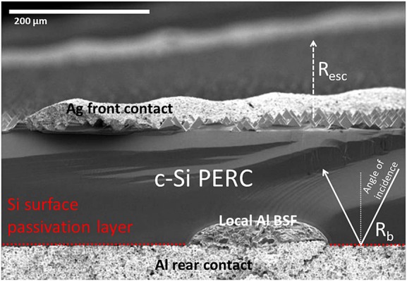
Scanning electron microscope cross-section image of a passivated emitter and rear c-Si solar cell, taken from 5. The front surface texturing is observable and the rear surface passivation layer is indicated (as the layer is too thin to be visible at this scale).
One of the main reasons to introduce such advanced technologies is to decrease the rear surface recombination velocity (Sb) and increase rear internal reflection (Rb), and consequently enhance the efficiency of ever thinner Si solar cells. The Si passivated emitter and rear solar cell design consists of a combination of a highly reflective rear surface passivation layer with micron-sized local point contacts, see, for example, Figure 1. It simultaneously functions as a passivation layer (reduction of Sb down to 100 cm/s) and a mirror (enhancement of Rb above 85%), while the point contacts allow for current collection. For a comprehensive reading on point contact opening characteristics and typical Si surface passivation layers, see 6. Hence, the excellent optical properties of such a dielectrically passivated rear surface (in combination with a textured front surface) result in superior light trapping, and thus allow reducing Si substrate thickness significantly, see, for example, 4,5.
Previously 6,7, it has been shown that a similar rear contacting structure can be used to passivate the rear CIGS interface of CIGS solar cells. The advanced cell design also combines a rear surface passivation layer and—as thin film solar cells have short minority carrier diffusion lengths—a technologically feasible approach to generate nano-sized local point contacts. Atomic layer deposition (ALD) of Al2O3 is used to passivate the CIGS rear surface, while the formation of nano-sphere shaped precipitates in chemical bath deposition (CBD) of CdS helps generating point contact openings in an industrially viable manner (top-view scanning electron microscope pictures of these local point openings can be found in 7). In this way, a 5 nm Al2O3 film with local point openings of about 220 nm is integrated in CIGS solar cells in 6. Compared with unpassivated reference solar cells, an obvious increase in open circuit voltage (Voc) is measured for the passivated cells 6,7. And, using solar cell capacitance simulator to model the Al2O3 rear surface passivated cells, the minimal Sb has been estimated to be as low as 100 cm/s 7. Note that Al2O3 is believed to be an adequate CIGS surface passivation layer due to similar arguments made as for its use as Si surface passivation layer 8–10: (i) first principles calculations indicate that the deposition of Al2O3 on CIGS reduces about 35% of the interface defect density, and (ii) Al2O3 exhibits a large density of negative charges, causing a field effect that effectively reduces the CIGS surface minority charge carrier concentration and consequently also the recombination at the Al2O3/CIGS interface.
In this contribution, the reflectance of this rear contacting structure is enhanced significantly, without reduction of its passivation properties. In 6, 5 nm of ALD Al2O3 increases Rb only slightly compared with the reference Mo/CIGS rear interface. Therefore, a more reflective rear surface passivation is required to increase short-circuit current (Jsc) and hence efficiency even further. In the succeeding text, two methods to increase Rb are demonstrated: (i) applying a thick sputtered Al2O3 layer and (ii) applying a MgF2/ALD-Al2O3 stack, both in combination with the CBD CdS point contacting approach described previously. This way, high average solar cell efficiencies are obtained for ultra-thin CIGS absorber layers. A complete analysis of these highly reflective rear surface passivated CIGS solar cells is presented, and compared to unpassivated reference CIGS solar cells.
2 EXPERIMENTAL
Soda lime glass (SLG)/Mo/CIGS/CdS/i-ZnO/ZnO:Al/MgF2 solar cell devices with thin CIGS absorber layers ([Cu]/([Ga] + [In]) = 0.85 to 0.90 and ungraded [Ga]/([Ga] + [In]) = 0.30) are used in combination with the developed rear surface passivation structures. A detailed description of standard CIGS solar cell processing at the Ångström Solar Center can be found in 11; that is excluding the ungraded absorber layer formation and the advanced back contact design. The starting substrate is low-iron soda lime glass with a thickness of 1 mm, which first undergoes a cleaning process. As back contact, a Mo layer is deposited in an inline sputtering system. It has a sheet resistance of 0.6 Ω/□ and a typical thickness of 350 nm. The advanced back contact design combines a rear surface passivation layer and CBD of CdS to generate nano-sized point openings, as described in next paragraphs. On top of this rear contact structure, first a 15 nm NaF layer is evaporated, followed by co-evaporation of the ungraded CIGS absorber layer of desired thickness. These ungraded CIGS absorbers with uniform low Ga concentration are favored to assess rear surface passivation, because of (i) their high reproducibility, (ii) their characteristic high minority carrier diffusion length, and (iii) to exclude complementary rear surface passivation effects (e.g., Ga-grading). The buffer layer is deposited using a standard CBD CdS process. Next, the shunt reducing intrinsic ZnO layer (i-ZnO), and subsequently the Al-doped ZnO (ZnO:Al) front contact are sputtered. As front contact grid, a Ni/Al/Ni stack is deposited by evaporation through a shadow mask. The ZnO and Ni/Al/Ni stack have a total thickness around 400 and 3000 nm, respectively. Finally, 0.5 cm2 solar cells are defined by mechanical scribing and a 110 nm MgF2 anti-reflective coating is evaporated (mainly to avoid interference fringes).
Evaporation of MgF2 coated with a thin ALD-Al2O3 layer, or direct current (DC-) magnetron sputtering of Al2O3 are integrated as rear surface passivation layers at the Mo/CIGS rear interface. The ALD Al2O3 passivation layers are deposited in a temporal ALD reactor at standard temperatures (300 °C) using trimethylaluminum and water (H2O) as precursors, resulting in a typical 1 Å/cycle growth rate. Additionally, Al2O3 films are also DC-sputtered from an Al (99.9%) target in an Ar/O2 gas mixture. These depositions are performed at room temperature and at constant total pressure, having a deposition rate of around 5 nm/min 12.
A previously developed CBD CdS contacting approach successfully generates nano-sized point openings in those (MgF2/)Al2O3 passivation layers. Earlier, it has been shown that for too thick ALD Al2O3 films the CdS point contacting approach becomes unsatisfactory 6. However, applying sputtering of Al2O3 or a thin film of ALD Al2O3 grown on evaporated MgF2 as passivation layers, the CdS nano-particles can still be removed to generate point openings; thanks to the directionality of sputtering and evaporation processes.
Table 1 gives an overview of all steps required to fabricate unpassivated reference CIGS solar cells, or (MgF2/)Al2O3 rear surface passivated cells with nano-sized local rear point contacts.
Table 1.
Overview of all steps required to fabricate unpassivated reference Cu(In,Ga)Se2 solar cells or (MgF2/)Al2O3 rear surface passivated cells with nano-sized local rear point contacts.
| Step | Unpassivated reference solar cells |
Rear passivated cells with local rear point contacts |
|
|---|---|---|---|
| (Al2O3 passivation) | (MgF2/Al2O3 passivation) | ||
| 1 | Glass cleaning | Glass cleaning | Glass cleaning |
| 2 | Mo rear contact sputt. | Mo rear contact sputt. | Mo rear contact sputt. |
| 3 | Particle-rich CdS depo. | Particle-rich CdS depo. | |
| 4 | DC-sputt. of Al2O3 | MgF2-evap./ALD-Al2O3 | |
| 5 | CdS particle removal | CdS particle removal | |
| 6 | NaF evap. | NaF evap. | NaF evap. |
| 7 | Ungraded CIGS co-evap. | Ungraded CIGS co-evap. | Ungraded CIGS co-evap. |
| 8 | CBD CdS buffer depo. | CBD CdS buffer depo. | CBD CdS buffer depo. |
| 9 | (i-)ZnO(:Al) window sputt. | (i-)ZnO(:Al) window sputt. | (i-)ZnO(:Al) window sputt. |
| 10 | Ni/Al/Ni front contact evap. | Ni/Al/Ni front contact evap. | Ni/Al/Ni front contact evap. |
| 11 | 0.5 cm2 solar cell scribing | 0.5 cm2 solar cell scribing | 0.5 cm2 solar cell scribing |
| 12 | MgF2 ARC evap. | MgF2 ARC evap. | MgF2 ARC evap. |
Illuminated J–V, external quantum efficiency (EQE) and transmission electron microscopy (TEM) measurements, and Rb calculations are performed as described elsewhere 6,7,11,13,14.
3 RESULTS AND DISCUSSION
3.1 Cross-section images
The realization of the applied point contact opening approach is confirmed in cross section pictures of rear passivated CIGS solar cells, revealing the (MgF2/)Al2O3 rear surface passivation layer and nano-sized local point openings. Figure 2 shows a cross section TEM image of a MgF2/Al2O3 rear surface passivated CIGS solar cell, where the rear surface passivation layer and a nano-sized local rear point contact are clearly visible. This picture is a first direct proof that the CBD CdS point contacting approach successfully generates nano-sized point openings of about 250 to 300 nm. Previously, the success of this point contacting approach has already been proven indirectly and the point openings estimated to be 220 ± 25 nm 7. Using TEM measurements, the average CIGS absorber (tCIGS), MgF2/Al2O3, and sputtered Al2O3 passivation layer thicknesses are estimated to be around 385, 65, and 25–50 nm, respectively.
Figure 2.
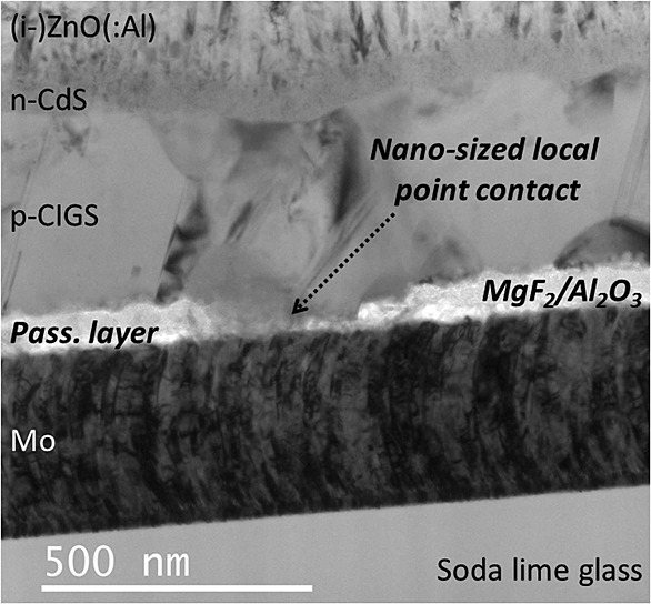
Transmission electron microscopy cross-section picture of an evaporated-MgF2/ALD-Al2O3 rear surface passivated Cu(In,Ga)Se2 solar cell with nano-sized local rear point contacts, where the rear surface passivation layer and a nano-sized local rear point contact are clearly visible.
3.2 Rear surface passivation and local point contacting analysis
Reducing CIGS absorber layer thickness leads to a drop in all solar cell characteristics for regular unpassivated solar cells, due to high Sb and low Rb of standard Mo/CIGS rear interfaces. Figure 3 and Table 2 provide average Voc, Jsc, fill factor (FF), and cell efficiencies for the MgF2/Al2O3 (65 nm) and for Al2O3 (25 or 50 nm) rear surface passivated ultra-thin CIGS (tCIGS = 385 nm) solar cells, compared with ultra-thin and thick (1800 nm) unpassivated reference cells. Additionally, representative J–V curves of all these solar cells can be found in Figure 4. The standard Mo/CIGS rear interface is known to show high Sb and low Rb, as discussed in 6. Therefore, the 0.4 µm thin reference cells display large losses in Voc and Jsc (and ultimately FF) compared with the 1.8 µm thick unpassivated reference cells, as the highly recombinative and lowly reflective Mo/CIGS rear interface gets closer to the most active region of the cells. These losses in Voc and Jsc can be reduced significantly by applying the advanced (MgF2/)Al2O3 rear contacting design, as is shown in the succeeding text.
Figure 3.
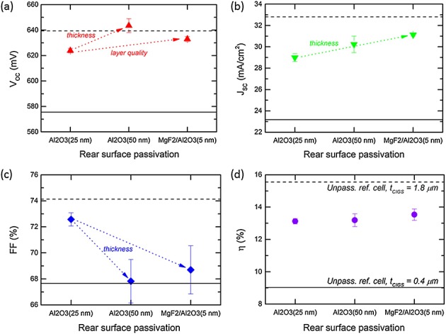
Average (a) open circuit voltage, (b) short circuit current, (c) fill factor, and (d) cell conversion efficiency for 0.5 cm2 unpassivated and (MgF2/)Al2O3 rear surface passivated Cu(In,Ga)Se2 solar cells. Standard deviation is shown as error bars.
Table 2.
Overview of average cell characterization results (AM1.5 G) for 0.5 cm2 unpassivated reference and (MgF2/)Al2O3 rear surface passivated Cu(In,Ga)Se2 solar cells, as also shown in Figure 3.
| Rear surface passivation | # cells | tCIGS (µm) | Voc (mV) | Jsc (mA/cm2) | FF (%) | η (%) |
|---|---|---|---|---|---|---|
| None | 6 | 0.4 | 576 ± 2 | 23.2 ± 0.3 | 67.7 ± 0.7 | 9.1 ± 0.1 |
| Sputt. Al2O3 (25 nm) | 6 | 0.4 | 624 ± 2 | 29.0 ± 0.4 | 72.6 ± 0.5 | 13.1 ± 0.2 |
| Sputt. Al2O3 (50 nm) | 6 | 0.4 | 644 ± 6 | 30.2 ± 0.8 | 67.8 ± 1.7 | 13.2 ± 0.4 |
| MgF2/ALD-Al2O3 (5 nm) | 6 | 0.4 | 633 ± 2 | 31.1 ± 0.1 | 68.7 ± 1.9 | 13.5 ± 0.4 |
| None | 6 | 1.8 | 639 ± 7 | 32.8 ± 0.5 | 74.1 ± 1.2 | 15.6 ± 0.7 |
Figure 4.
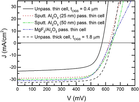
Representative J–V curves for 0.5 cm2 unpassivated and (MgF2/)Al2O3 rear surface passivated Cu(In,Ga)Se2 solar cells.
The (MgF2/)Al2O3 rear surface passivated solar cells have a higher Voc compared with the corresponding unpassivated reference cells, which can be explained by Al2O3 being an adequate surface passivation layer for CIGS interfaces. It is shown in 7,9 that Sb as low as 100 cm/s can be obtained at Al2O3/CIGS interfaces. Accordingly, an average Voc of 649 mV is obtained for ALD Al2O3 (5 nm) rear passivated CIGS solar cells in 6. Here, the average Voc of the MgF2/ALD-Al2O3 rear passivated cells equals 633 mV, thus somewhat lower than 649 mV. However, in 6, slightly thicker CIGS absorber layers (0.5 µm) have been used. On the other hand, the average Voc of the DC-sputtered Al2O3 rear passivated cells is quite low in case of a 25 nm Al2O3 passivation layer and increases as a function of Al2O3 thickness. This can be explained by DC-sputtering being a lower quality deposition technique compared with ALD. Nevertheless, increasing the thickness leads to enhanced passivation effect. For thick (50 nm) sputtered Al2O3 passivation layers, an average Voc of 644 mV is obtained, remarkably close to the 649 mV obtained in 6.
Thanks to the increase in Voc, the average FF is higher for (thin Al2O3) rear passivated solar cells than for the corresponding unpassivated reference cells. As a result of reduced rear surface recombination, thin Al2O3 rear passivated cells show a clear improvement in FF compared with unpassivated cells with equivalent CIGS thickness. Hence, an even larger FF should be expected for thick Al2O3 and MgF2/Al2O3 rear passivated cells. Unfortunately, the FF of the passivated cells decreases as a function of total passivation layer thickness as is shown in Figure 3(c). Also, the J–V curves presented in Figure 4 prove that this reduced FF in case of thick (MgF2/)Al2O3 passivation layers is caused by an increase in series resistance (Rs). This increase in Rs can be explained by a lack of contact openings for thicker passivation layers, as the CdS point contact opening approach becomes slightly less effective. Note that (i) a similar lack of contact openings for thick ALD Al2O3 passivation layers, (ii) but also regular J–V curves with low Rs for thin ALD Al2O3 (≤5 nm) rear passivated CIGS solar cells are shown in 6,7. Therefore, it is expected that applying well-ordered rear point contacting structures (using, e.g., e-beam lithography, work that is ongoing) in combination with thick (MgF2/)Al2O3 rear passivation layers will increase FF further (reduction of Rs), close to the FF of the thick unpassivated reference cells.
3.3 Rear internal reflection and absorption analysis
Applying “thick” (MgF2/)Al2O3 rear surface passivation layers enhances Rb considerably compared to standard Mo/CIGS rear interfaces. Figure 5 depicts Rb as a function of wavelength for a number of Mo(/CdS/MgF2)/Al2O3/CIGS devices and an unpassivated Mo/CIGS reference, calculated as in 7,14. This figure indicates that Rb is increased substantially by (i) increasing the thickness of the Al2O3 passivation layer, or (ii) stacking a thin Al2O3 interface passivation layer on top of another thick layer (e.g., MgF2). Note that it is thanks to the directionality of the sputtering and evaporation processes that the thick sputtered Al2O3 or evaporated MgF2 layers can be combined with the CdS contact opening approach.
Figure 5.
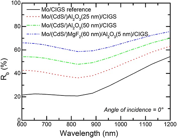
Calculated rear internal reflection as a function of wavelength for a variation of Mo(/CdS(5 nm)/MgF2)/Al2O3/Cu(In,Ga)Se2 devices and an unpassivated Mo/Cu(In,Ga)Se2 reference, see 13.
The increase in Rb for the rear passivated solar cells leads to an increase in Jsc, but there is still room for improvement. Figure 6 shows EQE measurements of representative unpassivated thin and thick CIGS solar cells, and rear surface passivated thin cells. The unpassivated reference cells demonstrate an expected loss in absorption for reduced CIGS absorber layer thickness, as Rb at the standard Mo/CIGS interface is rather low (and Sb high). However, this figure also shows that this loss can be substantially compensated by applying highly reflective (MgF2/)Al2O3 rear surface passivation layers. This way, photons reflected at the rear obtain an additional chance to be absorbed in the CIGS layer. Nevertheless, these rear surface passivated devices still show a reduction in EQE compared with thick unpassivated reference cells. Also, despite the significant difference in Rb for 50 nm of Al2O3 or 65 nm of MgF2/Al2O3 as rear surface passivation layer, both EQE graphs are very comparable for both passivation layers. Therefore, it is anticipated that this loss in EQE between the best passivated devices and the thick reference device is mainly caused by rear reflected photons escaping at the front surface of the solar cell, indicated as Resc in Figure 1. A very reasonable hypothesis as tCIGS is only 0.4 µm in case of the rear surface passivated cells, which equals to an apparent total tCIGS of 0.8 µm for rear reflected photons. Hence, absorption of all rear reflected photons is not expected, even if Rb would be 100%.
Figure 6.
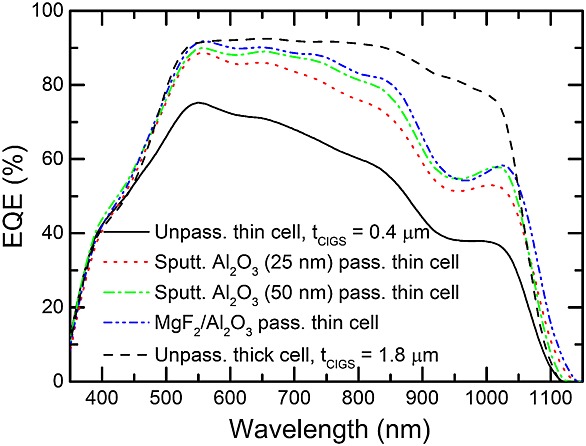
External quantum efficiency measurements of representative unpassivated and (MgF2/)Al2O3 rear surface passivated Cu(In,Ga)Se2 solar cells. All spectra are smoothed using a 50 point Savitzky-Golay smoothing filter 15.
3.4 Solar cell efficiencies
The cell efficiency of all passivated cells is noticeably higher than the efficiency of unpassivated reference cells with equivalent CIGS thickness, but still lower than the thick reference cell efficiency. Figure 3(d) shows that average cell efficiencies of rear passivated thin CIGS solar cells are between thin and thick unpassivated reference cell efficiencies: Higher than thin reference cells thanks to an increase in Voc and Jsc as explained in the preceding text, but still lower than thick reference cells because of residual losses in Jsc and FF. Compared with unpassivated thick reference cells, (i) thin Al2O3 passivated cells lack Jsc due to low Rb, and (ii) thick (MgF2/)Al2O3 passivated cells lose Jsc and FF due to high escape reflection (Resc) and non-optimal rear contacting, respectively.
4 CONCLUSIONS
This work studies progressive cell design concepts from Si solar industry to advance CIGS solar cell performance. Unconventional (MgF2/)Al2O3 rear surface passivated ultra-thin (tCIGS = 385 nm) CIGS solar cells with nano-sized local rear point contacts are developed, showing a significant increase in Voc and Jsc compared with corresponding unpassivated reference cells. This improvement in Voc and Jsc has been explained by Al2O3 being an adequate surface passivation layer for CIGS interfaces and the thick (MgF2/)Al2O3 layer being highly reflective, respectively. Accordingly, average solar cell efficiencies of 13.5% are realized for ultra-thin CIGS absorber layers, compared to 9.1% efficiency for the matching unpassivated reference cells. EQE measurements show a clear improvement in absorption of the passivated cells compared with the reference cells, but also indicate that—yet again analogous to Si solar cell design—further technological improvements can be made to increase Jsc even more. This proposed cell design appears to be more complex, but also holds the potential to reduce material/production costs (ever thinner absorber layers) and to increase solar cell efficiencies.
5 OUTLOOK
Compared with unpassivated reference cells with thick CIGS absorber layer, advances in optical confinement (or Jsc) and rear contacting structure (or FF) are still feasible. Jsc is expected to increase by (i) introducing textured rear or front surfaces and thus reducing Resc—as already done in advanced Si solar cell technologies, and (ii) increasing Rb even more. On the other hand, the FF is expected to increase by applying well-ordered rear point contacting structures. Therefore, (i) a complete analysis of the optical confinement to reduce Resc and increase Rb even further, and (ii) development of more controllable methods to generate nano-sized point contacts, for example, by use of e-beam lithography, laser ablation, or conductive Mo nano-particles, are ongoing. Additionally, (iii) Ga grading in the absorber layer is studied to increase absorption and surface passivation even further.
Moreover, more understanding of CIGS surface passivation layers is required. The work presented in 9 is a first attempt to understand the passivation mechanism(s) of Al2O3/CIGS interfaces. Therefore, (opto-)electrical characterization techniques as capacitance-voltage measurements of Mo/CIGS/Al2O3/Al structures and (time-resolved) photoluminescence measurements are applied to (iv) characterize the CIGS surface passivation layers developed within this work; equivalent to characterization methodologies applied in Si surface passivation research 8,10.
Acknowledgments
B. Vermang acknowledges the financial support of the European Commission via FP7 Marie Curie IEF 2011 Action No. 300998. Furthermore, this work is partly funded by the Swedish Science Foundation (VR) and the Swedish Energy Agency. Lastly, F. Henry would like to thank the European and Wallonia Region FEDER grant ECP12020011678F (MINATIS Project) for financial support.
REFERENCES
- Green MA, Emery K, Hishikawa Y, Warta W, Dunlop ED. Solar cell efficiency tables (version 43) Progress in Photovoltaics: Research and Applications. 2014;22:1–9. [Google Scholar]
- Chirilă A, Reinhard P, Pianezzi F, Bloesch P, Uhl AR, Fella C, Kranz L, Keller D, Gretener C, Hagendorfer H, Jaeger D, Erni R, Nishiwaki S, Buecheler S, Tiwari AN. Potassium-induced surface modification of Cu(In,Ga)Se2 thin films for high-efficiency solar cells. Nature Materials. 2013;12:1107–1111. doi: 10.1038/nmat3789. [DOI] [PubMed] [Google Scholar]
- Jackson P, Hariskos D, Lotter E, Paetel S, Wuerz R, Menner R, Wischmann W, Powalla M. New world record efficiency for Cu(In,Ga)Se2 thin-film solar cells beyond 20% Progress in Photovoltaics: Research and Applications. 2011;19:894–897. [Google Scholar]
- Zhao J, Wang A, Green MA, Ferrazza F. 19.8% efficient “honeycomb” textured multicrystalline and 24.4% monocrystalline silicon solar cells. Applied Physics Letters. 1998;73:1991–1993. [Google Scholar]
- Dullweber T, Gatz S, Hannebauer H, Falcon T, Hesse R, Schmidt J, Brendel R. Towards 20% efficient large-area screen-printed rear-passivated silicon solar cells. Progress in Photovoltaics: Research and Applications. 2012;6:630–638. [Google Scholar]
- Vermang B, Fjällström V, Gao X, Edoff M. Improved rear surface passivation of Cu(In,Ga)Se2 solar cells: a combination of an Al2O3 rear surface passivation layer and nanosized local rear point contacts. IEEE Journal of Photovoltaics. 2014;4:486–492. [Google Scholar]
- Vermang B, Fjällström V, Pettersson J, Salomé P, Edoff M. Development of rear surface passivated Cu(In,Ga)Se2 thin film solar cells with nano-sized local rear point contacts. Solar Energy Materials and Solar Cells. 2013;117:505–511. [Google Scholar]
- Dingemans G, Kessels WMM. Review: status and prospects of Al2O3-based surface passivation schemes for silicon solar cells. Journal of Vacuum Science & Technology A. 2012;30:040802. [Google Scholar]
- Hsu WW, Chen JY, Cheng TH, Lu SC, Ho WS, Chen YY, Chien YJ, Liu CW. Surface passivation of Cu(In,Ga)Se2 using atomic layer deposited Al2O3. Applied Physics Letters. 2012;100:023508. [Google Scholar]
- Vermang B. Aluminum oxide as negatively charged surface passivation for industrial crystalline silicon solar cells. Leuven: University of Leuven; 2012. ISBN: 978-94-6018-531-1. [Google Scholar]
- Lindahl J, Zimmermann U, Szaniawski P, Törndahl T, Hultqvist A, Salomé P, Platzer-Björkman C, Edoff M. Inline Cu(In,Ga)Se2 co-evaporation for high-efficiency solar cells and modules. IEEE Journal of Photovoltaics. 2013;3:1100–1105. [Google Scholar]
- Kotipalli R, Delamare R, Henry F, Proost J, Flandre D. 3Proc 28th EU PVSEC 2013, 1278–1281. Thermal stability analysis of DC-sputtered Al2O films for surface passivation of c-Si solar cells.
- Wätjen JT, Scragg JJ, Ericson T, Edoff M, Platzer-Björkman C. Secondary compound formation revealed by transmission electron microscopy at the Cu2ZnSnS4/Mo interface. Thin Solid Films. 2013;535:31–34. [Google Scholar]
- Duerinckx F, Kuzma-Filipek I, Van Nieuwenhuysen K, Beaucarne G, Poortmans J. Simulation and implementation of a porous silicon reflector for epitaxial silicon solar cells. Progress in Photovoltaics: Research & Applications. 2008;16:399–407. [Google Scholar]
- Schafer RW. What is a Savitzky-Golay filter? IEEE Signal Processing Magazine. 2011;28:111–117. [Google Scholar]


