Abstract
As highly sensitive H2S gas sensors, Au- and Ag-catalyzed SnO2 thin films with morphology-controlled nanostructures were fabricated by using e-beam evaporation in combination with the glancing angle deposition (GAD) technique. After annealing at 500 °C for 40 h, the sensors showed a polycrystalline phase with a porous, tilted columnar nanostructure. The gas sensitivities (S = Rgas/Rair) of Au and Ag-catalyzed SnO2 sensors fabricated by the GAD process were 0.009 and 0.015, respectively, under 5 ppm H2S at 300 °C, and the 90% response time was approximately 5 s. These sensors showed excellent sensitivities compared with the SnO2 thin film sensors that were deposited normally (glancing angle = 0°, S = 0.48).
Keywords: H2S sensor, nanosensor, SnO2 nanocolumn, glancing angle deposition
1. Introduction
Gas sensors have been used as detection devices for various gases in air. In particular, semiconductor gas sensors have proven to be very promising for monitoring the emission of gaseous species, and they represent a low-cost option compared to the standardized methods for ambient air classification, which require expensive and bulky equipment [1]. The gas-sensing mechanism of the semiconductor gas sensors is based on the resistance change of the sensor from the adsorption and desorption of the gases when specific gases interact with its surface [2]. Among the semiconducting metal oxides that are used for gas sensor applications, SnO2, n-type semiconducting metal oxide is the most widely studied material because it is sensitive to various gaseous species. In addition, gas sensors based on ZnO, In2O3, WO3, TiO2, Fe2O3, and others have also been investigated [3,4,5,6,7]. Especially, catalyzed SnO2 nanorod or nanowire-like structures were used as gas sensors with high sensitivities [8,9].
In terms of their application as hydrogen sulfide (H2S) gas sensors, the sensors based on SnO2 [10,11], WO3 [1,12], Fe2O3 [13], BaTiO3 [14], CuO-SnO2 composites [15,16,17,18], and CuO-WO3 composites [19] have been extensively studied. In these cases, many techniques have been used to study the adsorption and decomposition of H2S on the surface of metals such as Ag, Au, Pd, and Rh [20]; when Au films were used as the H2S sensor, their sensitivity was very low [21]. In addition, options including a chemiluminescent sensor and a colorimetric sensor, have been suggested as H2S sensors [22,23], and sensor-based methods for monitoring H2S and recent developments in H2S-sensing instrumentation were systematically reviewed [24].
H2S is widely used in various chemical industries and research laboratories, and is a very poisonous, corrosive, flammable, and explosive gas with the characteristic foul odor of rotten eggs. Exposure to lower concentrations can result in eye irritation, a sore throat and cough, nausea, shortness of breath, and fluid in the lungs. 10 ppm is the Occupational Safety and Health Administration (OSHA) permissible exposure limit (8 h time-weighted average) and 20 ppm is the acceptable ceiling concentration established by OOSHA [25]. H2S such as NO and CO is also produced in small amounts by some cells of the mammalian body and has a number of biological signaling functions. Accordingly, an accurate measurement and control of the H2S gases of low concentrations is very important to protect human lives.
In the present study, to enhance H2S gas-sensing characteristics, Au- and Ag-catalyzed SnO2 thin films with morphology-controlled nanostructures were fabricated by using e-beam evaporation in combination with the glancing angle deposition (GAD) technique. The GAD technique produces films with a high surface area that consist of isolated columns and provide excellent control over film/column morphology [26]. Use of e-beam GAD provides a method to control nanostructure unlike chemical vapor deposition, which is a non-line of sight deposition technique. By manipulating the tilt angles of the substrates and reaction-chamber oxygen pressures, it is possible to achieve a structural evolution from two-dimensional columnar films to one-dimensional nanorods, composites of nanorods and nanoparticles, and zero-dimensional nanoparticles [27,28]. X-ray diffraction (XRD) was used to analyze the films’ crystalline structure and the microstructures were observed using field emission scanning electron microscopy (FESEM). The sensors’ H2S sensing properties such as sensitivity and response time were subsequently measured and evaluated.
2. Experimental Procedure
To fabricate nanostructured sensors with a high reproducibility and easy mass production, metal-catalyzed SnO2 nanocolumns were deposited using the GAD technique.
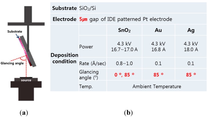
The substrate used for these sensors was the SiO2/Si wafer with Pt/Ti interdigitated electrodes (IDEs) that is comprised of an inter-electrode gap of 5 µm. The thicknesses of the Pt/Ti IDEs were 100 nm/50 nm, respectively, and IDEs were fabricated by photolithography and dry etching. SnO2 thin films of a 100 nm thickness (subsequently referred to as “SnO2 thin film sensor”) were deposited onto the substrate at an ambient temperature using an e-beam evaporator under 2 × 10⁻⁵ Torr. In the same manner, SnO2 thin films with nanocolumn morphology using the GAD technique (subsequently referred to as “SnO2 nanocolumn sensor”) were evaporated at a glancing angle of 85°, based on previous research [29]. The glancing vapor flux of atom randomly forms an initial nucleus like a nanoisland on the substrate. The initial nucleus makes a self-shadowed region that is not deposited on the opposite side of vapor flux. Next, continually growing up along one side by glancing vapor, the porous nanocolumns are formed on the tilt. In addition, Au or Ag of a 5 nm thickness was deposited onto the SnO2 nanocolumns. A schematic diagram of the e-beam evaporation as a function of the incident angle using the GAD technique and the details of the deposition conditions are shown in Figure 1. After the deposition, these thin films and nanocolumns were annealed at 500 °C for 40 h in air to produce SnO2 polycrystalline and metal nanoislands by aggregation.
Figure 1.
(a) A schematic diagram of the e-beam evaporation using the glancing angle deposition technique; (b) Deposition condition of the sensors.
The crystallinity and phase of the SnO2 films were characterized by a glancing angle X-ray diffractometer (D/Max-2500, Rikagu) with a 2θ scan from 20° to 80°, where Cu Kα (λ = 1.5414 Å) radiation was used for the X-ray source and the incident angle was fixed at 2°. The morphologies of the SnO2 films’ surfaces and cross-section were observed using an FESEM (FEI Inspect F50) operating at 8 kV.
The responses of these sensors to H2S gas were tested at 300 °C and changes of the sensor resistance were monitored during the transition from dry air to 5 ppm H2S gas balanced with N2 gas. To eliminate any interfering effects, a constant flow rate of 500 sccm was used for both the dry air and H2S gas conditions. Sensor resistances were measured at a DC bias voltage of 0.5 V using a source meter (Keithley 2400). Lastly, the H2S sensitivity and response time of the sensors were discussed.
3. Results and Discussion
3.1. Crystal Structure and Microstructures
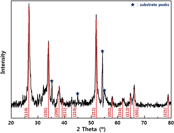
The XRD pattern of the SnO2 films is shown in Figure 2, and confirming that the as-deposited films were amorphous and the films annealed at 500 °C for 4 h were polycrystalline. The XRD peaks with a SnO2 tetragonal phase corresponded well with the JCPDS 41-1445 [30].
Figure 2.
X-ray diffraction pattern of the SnO2 thin film.
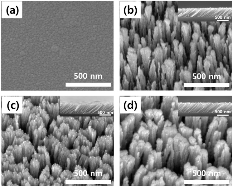
Surface and cross-sectional FESEM images of the SnO2 films are shown in Figure 3. Figure 3a shows an image of the SnO2 thin film (the film deposited at a glancing angle of 0°). The SnO2 thin film was relatively dense and was composed of a range of nanometer-sized grains. Alternatively, Figure 3b shows images of the SnO2 film deposited at a glancing angle of 85°, whereby its surface microstructure was nanoporous and a cross-sectional view revealed a tilted columnar structure. These results indicate that the nanocolumn sensors have larger sensor/gas contact areas than the thin film sensor of Figure 3a. As shown in Figure 3c,d, in the case of the Au- and Ag-catalyzed SnO2 nanocolumn sensors, the Au and Ag aggregated on the nanocolumn surface during the annealing process and a catalytic nanoisland was therefore formed.
Figure 3.
FESEM images. (a) Surface of SnO2 thin film (glancing angle = 0°); (b) Surface and cross-section of SnO2 thin film (glancing angle = 85°); (c) Surface and cross-section of Au-catalyzed SnO2 thin film (glancing angle = 85°); (d) Surface and cross-section of Ag-catalyzed SnO2 thin film (glancing angle = 85°).
3.2. Gas-Sensing Properties
Gas sensitivity (S) is defined here as Rgas/Rair, where Rgas is the resistance of the sensor in the H2S gas and Rair is its resistance in dry air.
At temperatures of 200–500 °C, metal oxides with n-type carrier paths, such as SnO2, ZnO, In2O3, and WO3, primarily respond to oxidizable gases such as H2, CH4, CO, and H2S, thereby increasing their conductivity [2]. It is well known that the surfaces of oxide semiconductors can adsorb oxygen from the ambient atmosphere. The chemisorbed oxygen species act as surface acceptors, trapping electrons and increasing the resistance of the metal oxides, as follows [31]:
| (1) |
| (2) |
| (3) |
The gas-sensing mechanism of the H2S gas can be explained by the reaction of the H2S on the SnO2 film in accordance with Equation (4); that is, the H2S rapidly reacts with the adsorbed oxygen and therefore releases the captured electrons back into the bulk. The surface reactions between the H2S and the oxygen species can be described in the following manner [31]:
| (4) |
The sensor resistance will therefore decrease when the SnO2 sensors are exposed to the H2S gas.
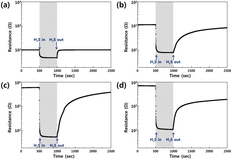
Figure 4 shows the H2S gas-sensing properties of the SnO2 sensors at an operating temperature of 300 °C and their sensitivities are summarized in Table 1. As shown in Figure 4a, the resistance of the SnO2 thin film sensor in dry air was 107.57 Ω (Rair), but its resistance when it was exposed to the 5 ppm H2S gas decreased to 51.23 Ω (Rgas), resulting in a gas sensitivity (S = Rgas/Rair) of 0.48. This change can be explained by Equation (4), and the result is similar to those from previous studies [32].
Figure 4.
Gas-sensing properties of the sensors exposed to 5 ppm H2S at 300 °C. (a) SnO2 thin film sensor; (b) SnO2 nanocolumn sensor; (c) Au-catalyzed SnO2 nanocolumn sensor; (d) Ag-catalyzed SnO2 nanocolumn sensor.
Table 1.
Resistance and H2S sensitivity of the sensors measured at 300 °C.
| SnO2 Thin Film | SnO2 Nanocolumn | Au-Catalyzed SnO2 Anocolumn | Ag-Catalyzed SnO2 Anocolumn | |
|---|---|---|---|---|
| Rair (Ω) | 107.57 | 1176.1 | 6209.5 | 7170.2 |
| Rgas* (Ω) | 51.23 | 83.9 | 56.87 | 111.9 |
| S = Rgas /Rair | 0.48 | 0.071 | 0.009 | 0.015 |
Rgas* = sensor resistance in 5 ppm H2S.
However, in the case of the SnO2 nanocolumn sensor fabricated by the GAD technique, the base resistance of the sensor in dry air had relatively high values that are approximately 10 times greater (Rair = 1176.1 Ω), and its H2S sensitivity was significantly enhanced (S = 0.071), as shown in Figure 4b; the SnO2 nanocolumn sensor shows very narrow and long, tilted columns with diameters of a few nanometers. This nanostructured shape increased the specific surface area that could react with gas, and adsorption of ionized oxygen species (O−, O2−, O2−) changed many regions of narrow necks between nanocolumns into the full depletion area (space charge layer); therefore, the resistance of the SnO2 nanocolumn sensor abruptly increased [29]. In the previous work, it was reported that the surface area of WO3 nanocolumnar thin film was about 32 times larger than that of a plain WO3 thin film by Brunauer-Emmett-Teller (BET) measurements [29]. This result shows which the increased surface area that can react to the gas will enhance the gas sensitivity. Moreover, it is also noted that the nano-sized narrow necks (10~30 nm) between the nanocolumns have a strong effect on the gas response [29]. Because the double Schottky barrier heights in the intergrain boundaries which are induced in the narrow neck region significantly increase, the sensitivity is dramatically enhanced by the change of conductance during the gas reaction [29]. We believe that these unique nanostructures as well as the increased surface area have an effect on the gas sensitivity.
The Au- and Ag-catalyzed SnO2 nanocolumn sensors had higher base resistances (Rair = 6209.5 Ω and 7171.6 Ω, respectively), as shown in Figure 4c,d. These higher values are due to the large depletion area that was formed by the trapping of electrons around the Au and Ag nanoislands, whose sensitivities were 0.009 and 0.015, respectively. As shown in Table 1, the base resistance of the Ag-SnO2 sensor is higher than that of the Au-SnO2 sensor, while the resistance change of the Ag-SnO2 sensor is lower and, therefore, its sensitivity has a higher value. It is assumed that the size of the Ag catalyst is relatively small compared to that of the Au catalyst and the Ag nanoislands cover the SnO2 nanocolumn surface; therefore, the reaction area of the nanocolumnar SnO2 with the H2S gas was decreased by the regions overspread with Ag nanoislands, which is called “catalytic filtering effect” [33].
Compared with the SnO2 thin film sensor that was fabricated normally with an e-beam evaporator, the sensitivity of the Au-catalyzed SnO2 nanocolumn sensor to 5 ppm H2S gas was enhanced 53 times.
The dynamic response and recovery curves of the sensors are also shown in Figure 4. When the H2S gas was injected, the sensors exhibited a fast response and a moderately slow recovery. The 90% response times of the sensors were approximately 41 s, 7 s, 5 s, and 6 s for Figure 4 a–d.
4. Conclusions
In the present study, e-beam evaporation was used in combination with the GAD technique to prepare highly sensitive H2S sensors. The gas-sensing material, SnO2 formed a polycrystalline tetragonal phase after annealing at 500 °C for 40 h. The surface morphology of the sensors that were fabricated by the GAD technique showed a porous, tilted columnar nanostructure. The Au-catalyzed SnO2 nanocolumn sensor showed an excellent sensitivity (S = 0.009 to the 5 ppm H2S at 300 °C) and a rapid response. We consider that the metal-catalyzed SnO2 nanocolumn sensors fabricated using the GAD process could be effectively used to detect low levels of H2S gas.
Acknowledgments
This work was supported by the 2014 Research Fund of the University of Seoul. Also, this work was supported by an Institute for Information & Communications Technology Promotion (IITP) Grant funded by the Korea Government (MSIP) (No. R0126-15-1050, Olfactory Bio Data Based Emotion Enhancement Interactive Content Technology Development).
Author Contributions
K.S.Y., C.-Y.K. and S.-J.Y. conceived and designed the experiments; S.D.H. performed the experiments; S.D.H. and H.G.M. analyzed the data; C.-Y.K. contributed reagents/materials/analysis tools; K.S.Y. and S.D.H. wrote the paper.
Conflicts of Interest
The authors declare no conflict of interest.
References
- 1.Ionescu R., Hoel A., Granqvist C.G., Llobet E., Heszler P. Low-level detection of ethanol and H2S with temperature-modulated WO3 nanoparticle gas sensors. Sens. Actuators B Chem. 2005;104:132–139. doi: 10.1016/j.snb.2004.05.015. [DOI] [Google Scholar]
- 2.Hauptmann P. Sensors: Principles & Application. Carl Hanser Verlag; Munich, German: 1993. pp. 115–153. [Google Scholar]
- 3.Korotcenkov G. Metal oxides for solid-state gas sensors: What determines our choice? Mater. Sci. Eng. B. 2007;139:1–23. doi: 10.1016/j.mseb.2007.01.044. [DOI] [Google Scholar]
- 4.Liu J., Guo Z., Zhu K., Wang W., Zhang C., Chen X. Highly porous metal oxide polycrystalline nanowire films with superior performance in gas sensors. J. Mater. Chem. 2011;21:11412–11417. doi: 10.1039/c1jm10537j. [DOI] [Google Scholar]
- 5.Korotcenkov G., Han S.-D., Cho B.K., Brinzari V. Grain size effects in sensor response of nanostructured SnO2- and In2O3-based conductometric thin film gas sensor. Crit. Rev. Solid State Mater. Sci. 2009;34:1–17. doi: 10.1080/10408430902815725. [DOI] [Google Scholar]
- 6.Huang J., Wan Q. Gas sensors based on semiconducting metal oxide one-dimensional nanostructures. Sensors. 2009;9:9903–9924. doi: 10.3390/s91209903. [DOI] [PMC free article] [PubMed] [Google Scholar]
- 7.Choi K.J., Jang H.W. One-dimensional oxide nanostructures as a gas-sensing materials: Review and issues. Sensors. 2010;10:4083–4099. doi: 10.3390/s100404083. [DOI] [PMC free article] [PubMed] [Google Scholar]
- 8.Arbiol J., Cirera A., Peiró F., Cornet A., Morante J.R., Delgado J.J., Calvino J.J. Optimization of tin oxide nanosticks faceting for the improvement of palladium nanocluster epitaxy. Appl. Phys. Lett. 2002;80:329–331. doi: 10.1063/1.1433903. [DOI] [Google Scholar]
- 9.Kolmakov A., Klenov D.O., Lilach Y., Stemmer S., Moskovits M. Enhanced gas sensing by individual SnO2 nanowires and nanobelts functionalized with Pd catalyst particles. Nano Lett. 2005;5:667–673. doi: 10.1021/nl050082v. [DOI] [PubMed] [Google Scholar]
- 10.Jin C., Yamazaki T., Ito K., Kikuta T., Nakatani N. H2S sensing property of porous SnO2 sputtered films coated with various doping films. Vacuum. 2006;80:723–725. doi: 10.1016/j.vacuum.2005.11.002. [DOI] [Google Scholar]
- 11.Liu C.H., Zhang L., He Y.-J. Properties and mechanism study of Ag doped SnO2 thin films as H2S sensors. Thin Solid Films. 1997;304:13–15. doi: 10.1016/S0040-6090(97)00107-7. [DOI] [Google Scholar]
- 12.Tao W.-H., Tsai C.-H. H2S sensing properties of noble metal doped WO3 thin film sensor fabricated by micromachining. Sens. Actuators B Chem. 2002;81:237–247. doi: 10.1016/S0925-4005(01)00958-3. [DOI] [Google Scholar]
- 13.Wang Y., Cao J., Kong F., Xia H., Zhang J., Zhu B., Wang S., Wu S. Low-temperature H2S sensor based on Ag-doped α-Fe2O3 nanoparticles. Sens. Actuators B Chem. 2008;131:183–189. doi: 10.1016/j.snb.2007.11.002. [DOI] [Google Scholar]
- 14.Jain G.H., Patil L.A., Wagh M.S., Patil D.R., Amalnerkar D.P. Surface modified BaTiO3 thick film resistors as H2S gas sensors. Sens. Actuators B Chem. 2006;117:159–165. doi: 10.1016/j.snb.2005.11.031. [DOI] [Google Scholar]
- 15.Chowdhuri A., Singh S.K., Sreenivas K., Gupta V. Contribution of adsorbed oxygen and interfacial space charge for enhanced response of SnO2 sensors having CuO catalyst for H2S gas. Sens. Actuators B Chem. 2010;145:155–166. doi: 10.1016/j.snb.2009.11.050. [DOI] [Google Scholar]
- 16.Katti V.R., Debnath A.K., Muthe K.P., Kaur M., Dua A.K., Gadkari S.C., Gupta S.K., Sahni V.C. Mechanism of drifts in H2S sensing properties of SnO2: CuO composite thin film sensors prepared by thermal evaporation. Sens. Actuators B Chem. 2003;96:245–252. doi: 10.1016/S0925-4005(03)00532-X. [DOI] [Google Scholar]
- 17.Vasiliev R.B., Rumyanantseva M.N., Yakovlev N.V., Gaskov A.M. CuO/SnO2 thin film heterostructures as chemical sensors to H2S. Sens. Actuators B Chem. 1998;50:186–193. doi: 10.1016/S0925-4005(98)00235-4. [DOI] [Google Scholar]
- 18.Chowdhuri A., Gupta V., Sreenivas K. Fast response H2S gas sensing characteristics with ultra-thin CuO islands on sputtered SnO2. Sens. Actuators B Chem. 2003;93:572–579. doi: 10.1016/S0925-4005(03)00226-0. [DOI] [Google Scholar]
- 19.Ramgir N.S., Goyal C.P., Sharma P.K., Goutam U.K., Bhattacharya S., Datta N., Kaur M., Debnath A.K., Aswal D.K., Gupta S.K. Selective H2S sensing characteristics of CuO modified WO3 thin films. Sens. Actuators B Chem. 2013;188:525–532. doi: 10.1016/j.snb.2013.07.052. [DOI] [Google Scholar]
- 20.Qin C., Whitten J.L. Interaction of S, SH, and H2S with Ag(100) Surf. Sci. 2005;588:83–91. doi: 10.1016/j.susc.2005.05.031. [DOI] [Google Scholar]
- 21.Yoo K.S., Sorensen I.W., Glaunsinger W.S. Adhesion, surface morphology, and gas sensing characteristics of thin-gold-film chemical sensors. J. Vac. Sci. Technol. A. 1994;12:192–198. doi: 10.1116/1.578880. [DOI] [Google Scholar]
- 22.Zhang Z., Jiang H., Xing Z., Zhang X. A highly selective chemiluminescent H2S sensor. Sens. Actuators B Chem. 2004;102:155–161. doi: 10.1016/j.snb.2004.04.015. [DOI] [Google Scholar]
- 23.Wallace K.J., Cordero S.R., Tan C.P., Lynch V.M., Anslyn E.V. A colorimetric response to hydrogen sulfide. Sens. Actuators B Chem. 2007;120:362–367. doi: 10.1016/j.snb.2006.02.031. [DOI] [Google Scholar]
- 24.Pandey S.K., Kim K.-H., Tang K.-T. A review of sensor-based methods for monitoring hydrogen sulfide. Trends Anal. Chem. 2013;32:87–99. doi: 10.1016/j.trac.2011.08.008. [DOI] [Google Scholar]
- 25.Hydrogen Sulfide. [(accessed on 12 May 2015)]. Available online: http://en.wikipedia.org/wiki/hydrogen_sulfide.
- 26.Robbie K., Brett M.J. Sculptured thin films and glancing angle deposition: Growth mechanisms and applications. J. Vac. Sci. Technol. A. 1997;15:1460–1465. doi: 10.1116/1.580562. [DOI] [Google Scholar]
- 27.Sit J.C., Vick D., Robbie K., Brett M.J. Thin film microstructure control using glancing angle deposition by sputtering. J. Mater. Res. 1999;14:1197–1199. doi: 10.1557/JMR.1999.0162. [DOI] [Google Scholar]
- 28.Tsoi S., Fok E., Sit J.C., Veinot J.G.C. Surface functionalization of porous nanostructured metal oxide thin film fabricated by glancing angle deposition. Chem. Mater. 2006;18:5260–5266. doi: 10.1021/cm061709t. [DOI] [Google Scholar]
- 29.Moon H.K., Choi Y.R., Shim Y.-S., Choi K.-I., Lee J.-H., Kim J.-S., Yoon S.-J., Park H.-H., Kang C.-Y., Jang H.W. Extremely sensitive and selective NO probe based on villi-like WO3 nanostructures for application to exhaled breath analyzers. Appl. Mater. Interfaces. 2013;5:10591–10596. doi: 10.1021/am402456s. [DOI] [PubMed] [Google Scholar]
- 30.McCarthy G., Welton J. X-Ray Diffraction Data for SnO2- An Illustration of the New Powder Data Evaluation Methods. Powder Diffr. 1989;4:156–159. doi: 10.1017/S0885715600016638. [DOI] [Google Scholar]
- 31.Kapse V.D., Ghosh S.A., Chaudhari G.N., Raghuwanshi F.C. Nanocrystalline In2O3-based H2S sensors operable at low temperatures. Talanta. 2008;76:610–616. doi: 10.1016/j.talanta.2008.03.050. [DOI] [PubMed] [Google Scholar]
- 32.Gong J., Chen Q., Lian M.-R., Liu N.-C., Stevenson R.G., Adami F. Micromachined nanocrystalline silver doped SnO2 H2S sensor. Sens. Actuators B. Chem. 2006;114:32–39. doi: 10.1016/j.snb.2005.04.035. [DOI] [Google Scholar]
- 33.Portnoff M.A., Grace R., Guzman A.M., Runco P.D., Yannopoulos L.N. Enhancement of MOS gas sensor selectivity by ‘on-chip’ catalytic filtering. Sens. Actuators B. Chem. 1991;5:231–235. doi: 10.1016/0925-4005(91)80253-G. [DOI] [Google Scholar]


