Abstract
The time-dependent dielectric breakdown (TDDB) in on-chip interconnect stacks is one of the most critical failure mechanisms for microelectronic devices. The aggressive scaling of feature sizes, both on devices and interconnects, leads to serious challenges to ensure the required product reliability. Standard reliability tests and post-mortem failure analysis provide only limited information about the physics of failure mechanisms and degradation kinetics. Therefore it is necessary to develop new experimental approaches and procedures to study the TDDB failure mechanisms and degradation kinetics in particular. In this paper, an in situ experimental methodology in the transmission electron microscope (TEM) is demonstrated to investigate the TDDB degradation and failure mechanisms in Cu/ULK interconnect stacks. High quality imaging and chemical analysis are used to study the kinetic process. The in situ electrical test is integrated into the TEM to provide an elevated electrical field to the dielectrics. Electron tomography is utilized to characterize the directed Cu diffusion in the insulating dielectrics. This experimental procedure opens a possibility to study the failure mechanism in interconnect stacks of microelectronic products, and it could also be extended to other structures in active devices.
Keywords: Engineering, Issue 100, Time-dependent dielectric breakdown, reliability, copper interconnect, degradation kinetics, in situ TEM, ultra-low-k (ULK) material
Introduction
Since Cu interconnects were firstly introduced into the ultra-large-scale integration (ULSI) technology in 1997 1, low-k and ultra-low-k (ULK) dielectrics have been adopted into the back-end-of-line (BEoL) as the insulating materials between on-chip interconnects. The combination of new materials, e.g., Cu for reduced resistance and low-k/ULK dielectrics for lower capacitance, overcomes the effects of increased resistance-capacitance (RC) delay caused by interconnect dimensional shrinkage 2, 3. However, this benefit was encroached by the continuing aggressive scaling of microelectronic devices in recent years. The use of low-k/ULK materials results in various challenges in the manufacturing process and for the product reliability, particularly if the interconnect pitch reaches about 100 nm or less 4-6.
TDDB refers to the physical failure mechanism of a dielectric material as a function of time under an electric field. The TDDB reliability test is usually carried out under accelerated conditions (elevated electrical field and/or elevated temperature).
The TDDB in on-chip interconnect stacks is one of the most critical failure mechanisms for the microelectronic devices, which has already raised intense concerns in the reliability community. It will continue to be in the spotlight of reliability engineers since ULK dielectrics with even weaker electrical and mechanical properties are being integrated into the devices in advanced technology nodes.
Dedicated experiments have been performed to investigate the TDDB failure mechanism 7-9, and a significant amount of effort has been invested to develop models which describe the relationship between electric field and lifetime of the devices 10-13. The existing studies benefit the community of reliability engineers in microelectronics; however, many challenges still exist and many questions still need to be answered in detail. For example, proven models to describe the physical failure mechanism and degradation kinetics in the TDDB process and the respective experimental verification are still lacking. As a particular need, a more appropriate model is needed to substitute the conservative √E-model 14.
As a very important part of the TDDB investigation, typical failure analysis is facing an unprecedented challenge, i.e., providing comprehensive and hard evidence to explain the physics of failure mechanisms and degradation kinetics. Apparently, inspecting millions of vias and meters of nanoscale Cu lines one by one and ex situ imaging the failure site is not the appropriate choice to hurdle this challenge, because it is very time consuming, and only limited information about the kinetics of the damage mechanism can be provided. Therefore, an urgent task has emerged to develop and to optimize experiments and to get a better procedure to study the TDDB failure mechanisms and degradation kinetics.
In this paper, we will demonstrate an in situ experimental methodology to investigate the TDDB failure mechanism in Cu/ULK interconnect stacks. A TEM with the ability of high quality imaging and chemical analysis is used to study the kinetic process at dedicated test structures. The in situ electrical test is integrated into the TEM experiment to provide an elevated electrical field to the dielectrics. A customized “tip-to-tip” structure, consisting of fully encapsulated Cu interconnects and insulated by a ULK material, is designed in the 32 nm CMOS technology node. The experimental procedure described here can also be extended to other structures in active devices.
Protocol
1. Preparing the Sample for the Focused Ion Beam (FIB) Thinning (Figure 1)
Cleave the full wafer into small chips (~ 10 mm by 10 mm) with a diamond scribe.
Mark the positions of the “tip-to-tip” structure on the chips.
Saw the chip with a dicing machine to obtain bars of 60 µm by 2 mm size. The bar includes the “tip-to-tip” structure in the center.
Glue the target bar on a Cu half ring using the super glue. Next, glue the bar on a Cu sample stage also using the super glue. Then, use silver paste to set the conduction between the half ring and the copper sample stage. Note: When handling the sample, make sure to always wear an antistatic wrist strap to prevent electrostatic discharges, which may damage the sensitive structure in the sample.
2. FIB Thinning in the Scanning Electron Microscope (Figure 2)
Put the sample obtained in step 1 on an SEM sample stage and place the stage carefully into the SEM.
- Chose the deposition mode, and set up the dimensions (area and thickness) of the needed Pt protection layer. Always use a 30 kV ion beam to maintain the highest precision. Tune the current to get the satisfied efficiency, dependent on the dimensions of the needed Pt layer.
- Deposit a Pt line to contact one pad to the Cu stage (ground potential). Subsequently, deposit a thick Pt layer on top of the “tip-to-tip” structure, which is very important to minimize the ion damage during the FIB thinning process and to reinforce the thin lamella. This is a standard procedure used in FIB preparation.
- Take caution not to introduce any conductive paths between the two pads on top of the “tip-to-tip” structure through the Pt layer when performing the Pt deposition. Any conductive path will short the electrical circuit (Figure 2A and B).
- FIB milling
- Use a voltage of 30 kV and current of 10 pA for the final cut. Thin the target bar into an H-bar TEM lamella with a thickness between 150 and 180 nm.
- Cut a notch close to the pad (V+ pad) which will be touched by a transducer tip in the TEM. Use the notch as a marker to identify the correct pad in the TEM.
3. Sample Transfer from the SEM to the TEM
Put on the antistatic wrist strap before touching the sample.
Dismount the prepared H-bar sample from the SEM stage. Keep the sample on the Cu stage when removing it from the SEM.
- Fix the Cu stage onto the TEM holder. Move the transducer tip of the TEM holder close to the test structure (a few hundreds of micrometers away from the test structure) under the optical microscope.
- Insert the TEM holder into the TEM carefully. Do not utilize any cleaning treatment (e.g., plasma cleaning) during the transfer process, otherwise the lamella may be influenced.
Keep the time for the sample transfer within 15 min or shorter to avoid too much exposure to ambient moisture and oxygen.
4. Establishing the Electrical Connection (Figure 3)
Connect the TEM holder to its control system and the SourceMeter. Then switch on the control system and the SourceMeter.
- Monitor the transducer tip in the TEM when doing the coarse approach of the transducer tip to the test structure by tuning the knobs on the TEM holder.
- Move the transducer tip of the TEM holder close to the V+ pad (≤ 500 nm). Bring the transducer tip to the same level (Z: height) as the pad. Tune the position of the tip and make the tip face the center of the V+ pad.
Contact the transducer tip to the V+ pad. Set a very low voltage on the tip (0.5 V to about 1 V) while approaching the pad. Monitor the current simultaneously to make sure the contact is established.
5. In Situ TDDB Experiment
Use an accelerated voltage of 200 kV in the TEM. Move the electron beam to the area of interest; choose a proper magnification and focus the image.
Use low illumination steps (≤ 8) to reduce the beam damage on the test structure. Use a condenser aperture to localize the illumination area only within the thin part of the H-bar sample.
Apply a constant voltage (≤ 40 V) on the “tip-to-tip” structure using the SourceMeter while recording the TEM images in situ (2-3 frames/sec). Record the images automatically by using a self-scripted code, e.g., using the DigitalMicrograph software.
- Pause the experiment when seeing an apparent diffusion of metal into the ULK dielectrics and do the Electron Spectroscopic Imaging (ESI) chemical analysis.
- Insert the filter slit aperture into the Omega energy filter in the TEM.
- Tune the width of the filter silt aperture to get a proper energy width (10–20 eV) in the electron energy loss spectrum (EELS).
- Shift the energy to the copper M-edge adsorption peak in the EELS.
- Go back to the imaging mode to acquire an energy filtered TEM image at the Cu M-edge absorption peak.
- Shift the energy to the pre-edge of the copper M-edge and get another energy filtered TEM image.
- Correct the drift of the sample between the two images.
- Divide the first image by the second one to get the jump ratio image of Cu.
Continue the TDDB experiment: reapply a constant voltage (≤ 40 V) on the “tip-to-tip” structure using the SourceMeter and record the TEM images.
6. Computed Tomography
Perform TEM computed tomography when the TDDB experiment is finished, to get 3D distribution information about the diffused particles.
Tilt the sample and record a tilt series of 138°. Use a tilt step of 1°, and record the image during every step in the bright field (BF) STEM mode.
Reconstruct the series (includes aligning images, determining tilt axis, reconstructing volume and segmentation to form the 3D tomographic volume).
Representative Results
Figure 4 shows bright field (BF) TEM images from an in situ test. There are partially breached TaN/Ta barriers and pre-existing Cu atoms in the ULK dielectrics before the electrical test (Figure 4A) due to extended storage in ambient. After only 376 sec at 40 V, the dielectric breakdown started and was accompanied with two major migration pathways of copper from the M1 metal, having a positive potential with reference to the ground side 15-16. The diffused Cu particles in the ULK dielectrics are shown in the BF TEM image after the final breakdown (Figure 4B).
In a flawless sample, i.e., fast transfer between FIB preparation and TEM imaging (Figure 5A), the “tip-to-tip” structure is intact without any damage in the TaN/Ta barrier. The same voltage (40 V) was applied to this sample. This sample survived for more than 50 min until the breakdown occurred because of the intact TaN/Ta barrier. The TEM image after breakdown is shown in Figure 5B. Apparently, metal atoms migrated into the SiO2 from the bottom corner of the M1 metal, having a positive potential indicated by a red arrow 17. The ESI chemical analysis (Figure 5C) proves that there is a migration path of Cu at the fracture interface between the SiCN layer and the ULK dielectrics, which could not be detected from the contrast of the BF TEM image in Figure 5B. The combination of the ESI chemical analysis and in situ TDDB experiment in the TEM enables an investigation of the TDDB failure mechanism and degradation kinetics 15-16 in a more direct and comprehensive way.
Tomography is a choice to characterize the 3D distribution of Cu particles which diffused out from the positive side of the “tip-to-tip” structure. Figure 6B depicts a slice of a 3D-rendering of the sample acquired by computed tomography in the TEM. The yellow particles represent the migrated Cu particles in the SiO2.
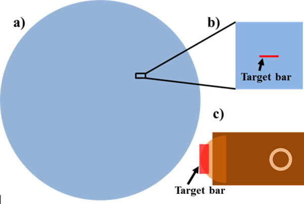 Figure 1.Schematic images of the experiment before the sample is put into the scanning electron microscope (SEM). (A) A full wafer. (B) A chip from the full wafer. (C) A target bar with a “tip-to-tip” structure on a Cu half ring which is glued on a sample stage. Please click here to view a larger version of this figure.
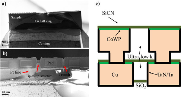 Figure 2.An H-bar sample fabricated by the focused ion beam (FIB) technique in the SEM and a schematic image of the “tip-to-tip” structure. (A) and (B) in the SEM. (C) The schematics of a “tip-to-tip” structure. Please click here to view a larger version of this figure.
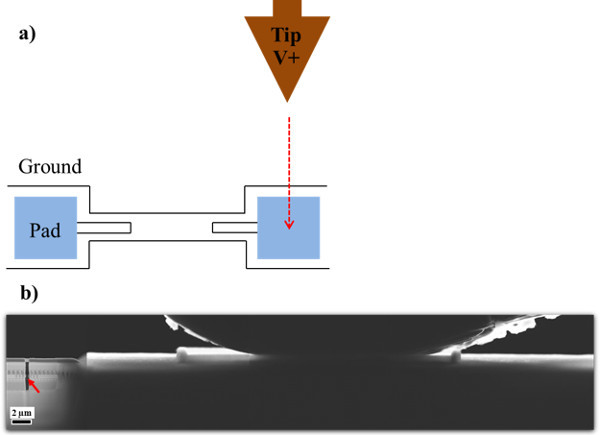 Figure 3.Experimental setup in the transmission electron microscope (TEM). (A) Schematic image of the contact approaching process. (B) STEM image of the setup before the in situ TDDB experiment. Please click here to view a larger version of this figure.
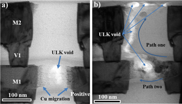 Figure 4. Representative TEM images for a “tip-to-tip” structure with diffused Cu into the ULK dielectrics before the in situ experiment. (A) Before the electrical test. (B) After the electrical test. Please click here to view a larger version of this figure.
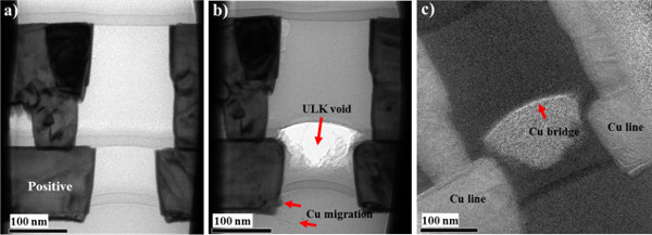 Figure 5.Representative TEM images for a flawless “tip-to-tip” structure. (A) Bright field (BF) TEM image before the electrical test. (B) BF TEM image after the electrical test. (C) Electron spectroscopic image of the Cu distribution. Please click here to view a larger version of this figure.
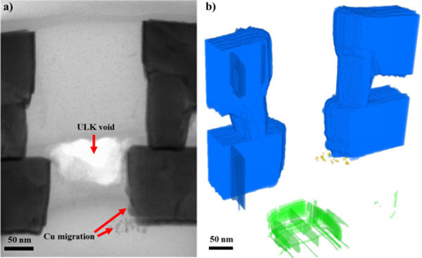 Figure 6.STEM image and 3D-rendering of a “tip-to-tip” structure after the electrical test. (A) STEM image. (B) 3D-rendering of the sample acquired by computed tomography in the TEM (Blue: “Tip-to-tip” structure, Yellow: Cu particles, Green: Transistor structure beneath).
Discussion
The prerequisite of success in the TDDB experiment is good sample preparation, especially in the FIB milling process in the SEM. Firstly, a thick Pt layer on top of the “tip-to-tip” structure has to be deposited. The thickness and the size of the Pt layer can be adjusted by the SEM operator, but have to follow three principles: (1) The thickness and the size are enough to protect the target area from possible ion beam damage during the whole milling process; (2) There is still a relatively thick Pt layer (≥ 400 nm) on top of the sample left after the milling, it protects the delicate sample from internal and external stresses and minimizes the contribution of stress to the dielectric breakdown in the next TDDB experiment; (3) The size should not be too big, otherwise a conductive path may form between the two pads which are used to apply the voltage to the test structure. Furthermore, the key step is when to stop the ion beam of the final cut. The ion milling must be interrupted immediately once a specifically designed Cu “dummy” interconnect structure in front of the test structure disappears, because the central Cu interconnects consist of the “tip-to-tip” structure and there is only ~ 60 nm space between them. It will be too late if the “tip-to-tip” structure appears in the live SEM image. The thickness of the H-bar TEM lamella is targeted to be about 150 to 180 nm. This thickness allows electron transparency in the TEM at 200 kV acceleration voltage and also keeps a relatively thick dielectric on the sides which encapsulate the “tip-to-tip” structure. On the other hand, the sample thicknesses of 150–180 nm will cause significant multiple inelastic scattering during the ESI chemical analysis, therefore these effects need to be considered into the result analysis as well.
When handling or transferring the sample, wear an antistatic wrist strap. This is very important, since electrostatic discharge damage on several samples was observed in our experiment if the antistatic wrist strap was not worn. The most crucial transfer step is the transfer from the SEM to the TEM. The transfer time has to be strictly restricted within 15 min or less. A long time exposure of the sample in ambient air may absorb moisture and damage the “tip-to-tip” structure, an example is shown in Figure 4A. This sample was stored in ambient air for two weeks before the test. The breached TaN/Ta barrier influences the intrinsic failure mechanism and shortens the lifetime of the test structure. Massive Cu diffusion is then enabled.
One concern for the in situ TDDB study in the TEM is the beam damage on the ULK dielectrics. Therefore, it is very crucial to minimize the influence of the beam on the experiment 18. Several strategies can be chosen to reduce this influence, but it cannot be eliminated completely. The options could be categorized into three approaches. One possibility is using a small condenser aperture to reduce the total amount of energy deposited in the H-bar type sample 18. The other option is operating the TEM at low voltage (≤ 80 kV) 19-21 and/or low electron dose 22-25. This option is expected to directly reduce the beam damage on the sample. Furthermore, the scanning TEM (STEM) mode can be a low-dose microscopy technique as well, if the experimental parameters are chosen correctly. Thus, the STEM mode should be prioritized if it is a possible option in the TEM used. Choosing low illumination brightness and recording the TEM images with a chosen, reasonable interval time (low dose) are also recommended 18 to result in further reduced beam damage.
Apart from the intrinsic TDDB, the TEM sample preparation and the TEM observation could theoretically affect the final breakdown. Nevertheless, the TDDB damage mechanism observed is believed to be valid because: (1) with much less TEM beam irradiation (low-dose STEM imaging, low illumination step and recording images every 30 min/1 h), the test sample showed similar failure mechanisms as in our previous TEM observation (recording images continuously, relatively high-dose TEM mode) 16-18; (2) the electrical field was confirmed as the driving force and the origin of the migration of metal particles 17 (Figure 5B and 6A) by reversing the electrical connection; (3) migration of metal particles and dielectric breakdown were both observed at specific locations where the tip-to-tip spacing is relatively small and the Ta/TaN barrier is relatively thin, not everywhere inside the illumination area of the TEM beam; (4) a thick layer of Pt deposition on top of the sample prevents most of the contamination from the vertical implantation of Ga ions — the test structure is believed to be mainly contamination free even if there is a slight amount of contamination on the surface of the side walls (about 60 nm) from the lateral damage of the Ga ions. Therefore, the sample preparation and the TEM observation should not affect the interpretation of the intrinsic failure mechanism to a significant amount.
The need of sophisticated procedures for sample preparation and the experimental setup is probably the main disadvantage. This methodology is only applicable for the specifically designed test structure. Therefore, the design and the complicated fabrication process for the dedicated test structure lead to quite more efforts when compared to conventional testing methodologies. Finally, it is worth pointing out that the modification of the sample by beam irradiation in the TEM is inevitable if the electron beam illuminates the delicate sample for a very long time. Nevertheless, we believe that this methodology can enable the study of TDDB failure mechanisms and degradation kinetics.
Further development on the experiment may be able to provide quantitative data for the Cu migration in the dielectrics as a function of applied voltage and/or time and help to develop a more appropriate model for the Cu/ULK on-chip interconnect stacks. In our study, the ESI signal of a Cu bridge at the bottom of the SiCN layer as shown in Figure 5C clearly points to the fact that Cu most likely diffused along the main dielectric/SiCN interface. This top surface of the main dielectric is affected by the planarization process and is expected to have the highest amount of imperfections/defects, then leading to a relatively weak interface with the SiCN layer. Diffusional processes, enabling significant Cu movement, should occur there. The electronic conduction mechanism, preceding the Cu diffusion and leading to dielectric damage, should follow Poole-Frenkel behavior, therefore favoring the √E-model. A deviation from this model cannot be deduced with the here proposed experimental method yet due to the large biases needed to enable reasonable testing times. It should be noted though that lowering the applied voltages and resulting electrical fields should be one of the future tasks in refining the here described experimental methodology. Actual chip operating biases are on the order of 1 to 3 V. The here applied voltages are quite higher, therefore other effects may play a more dominant role at the elevated voltages. To this end, new test structures were designed which have a significantly reduced spacing on the order of 20 to 50 nm. Then, smaller voltages can be applied and experimental data can still be acquired in a reasonable amount of time. The movement of Cu, possibly eliminated at low biases due to the existence of a threshold for dielectric damage to occur, could then be characterized as a function of applied bias and time. These efforts will be part of a forthcoming study and could prove or disprove the impact damage model, which from a physical damage mechanism perspective is currently the most likely model to describe TDDB effects at low biases 10.
Transmission X-Ray Microscopy (TXM) could be adopted for this experiment as well if the spatial resolution could be improved to much less than 10 nm. More importantly, better transmission ability and lower radiation dose than in the TEM may boost its application on other active microelectronic devices.
Disclosures
No competing financial interests.
Acknowledgments
The authors would like to thank Rüdiger Rosenkranz and Sven Niese (Fraunhofer IKTS-MD) for their assistance in sample preparation, and Ude Hangen, Douglas Stauffer, Ryan Major and Oden Warren (Hysitron Inc.) for their technical support on the PI95 TEM holder. The support of the Center for Advancing Electronics Dresden (cfaed) and the Dresden Center for Nanoanalysis (DCN) at Technische Universität Dresden is acknowledged as well.
References
- Edelstein D, et al. Full Copper Wiring in a Sub-0.25 µm CMOS ULSI Technology. IEDM Tech. Dig. 1997. pp. 773–776.
- List S, Bamal M, Stucchi M, Maex K. A global view of interconnects. Microelectron. Eng. 2006;83(11/12):2200–2207. [Google Scholar]
- Meindl JD, Davis JA, Zarkesh-Ha P, Patel CS, Martin KP, Kohl PA. Interconnect opportunities for gigascale integration. IBM J. Res. Develop. 2002;46(2/3):245–263. [Google Scholar]
- Zhang XF, Wang YW, Im JH, Ho PS. Chip-Package Interaction and Reliability Improvement by Structure Optimization for Ultralow-k Interconnects in Flip-Chip Packages. IEEE Trans. Device Mater. Reliab. 2012;12(2):462–469. [Google Scholar]
- Lee KD, Ogawa ET, Yoon S, Lu X, Ho PS. Electromigration reliability of dual-damascene Cu/porous methylsilsesquioxane low k interconnects. Appl. Phys. Lett. 2003;82(13):2032. [Google Scholar]
- Zschech E, et al. Stress-induced phenomena in nanosized copper interconnect structures studied by x-ray and electron microscopy. J. Appl. Phys. 2009;106(9):093711. [Google Scholar]
- Tan TL, Hwang N, Gan CL. Dielectric Breakdown Failure Mechanisms in Cu-SiOC low-k interconnect system. IEEE Trans. Bimodal. 2007;7(2):373–378. [Google Scholar]
- Zhao L, et al. Direct observation of the 1/E dependence of time dependent dielectric breakdown in the presence of copper. Appl. Phys. Lett. 2011;98(3):032107. [Google Scholar]
- Breuer T, Kerst U, Boit C, Langer E, Ruelke H, Fissel A. Conduction and material transport phenomena of degradation in electrically stressed ultra-low-k dielectric before breakdown. J. Appl. Phys. 2012;112(12):124103. [Google Scholar]
- Lloyd JR, Liniger E, Shaw TM. Simple model for time-dependent dielectric breakdown in inter- and intralevel low-k dielectrics. J. Appl. Phys. 2005;98(8):084109. [Google Scholar]
- Chen F, et al., editors. A Comprehensive Study of Low-k SiCOH TDDB Phenomena and Its Reliability Lifetime Model Development. 44th Annual International Reliability Physics Symposium Proceedings; 2006 Mar 26-30; San Jose, California. 2006. pp. 46–53. [Google Scholar]
- Wu W, Duan X, Yuan JS. Modeling of Time-Dependent Dielectric Breakdown in Copper Metallization) IEEE Trans. Device Mater. Reliab. 2003;3(2):26–30. [Google Scholar]
- Achanta RS, Plawsky JL, Gill WN. A time dependent dielectric breakdown model for field accelerated low-k breakdown due to copper ions. Appl. Phys. Lett. 2007;91(23):234106. [Google Scholar]
- Chen F, Shinosky M. Soft breakdown characteristics of ultralow-k time-dependent dielectric breakdown for advanced complementary metal-oxide semiconductor technologies. J. Appl. Phys. 2010;108(5):054107. [Google Scholar]
- Yeap KB, et al., editors. An Experimental Methodology for the In-Situ Observation of the Time-Dependent Dielectric Breakdown Mechanism in Copper/Low-k On-Chip Interconnect Structures. 51st Annual International Reliability Physics Symposium.2013. [Google Scholar]
- Yeap KB, et al. In situ study on low-k interconnect time-dependent-dielectric-breakdown mechanisms) J. Appl. Phys. 2014;115(12):124101. [Google Scholar]
- Liao ZQ, et al. In-situ Study of the TDDB-Induced Damage Mechanism in Cu/Ultra-low-k Interconnect Structures. Microelectron. Eng. 2014;In Press [Google Scholar]
- Liao ZQ, et al. A New In Situ Microscopy Approach to Study the Degradation and Failure Mechanisms of Time-Dependent Dielectric Breakdown: Set-Up and Opportunities. Adv. Eng. Mater. 2014;16(5):486–493. [Google Scholar]
- Lee Z, Meyer JC, Rose H, Kaiser U. Optimum HRTEM image contrast at 20 kV and 80 kV-Exemplified by graphene. Ultramicroscopy. 2012;112(1):39–46. doi: 10.1016/j.ultramic.2011.10.009. [DOI] [PubMed] [Google Scholar]
- Bell DC, Russo CJ, Kolmykov DV. 40 keV atomic resolution TEM. Ultramicroscopy. 2012;114:31–37. doi: 10.1016/j.ultramic.2011.12.001. [DOI] [PubMed] [Google Scholar]
- Kaiser U, et al. Transmission electron microscopy at 20 kV for imaging and spectroscopy. Ultramicroscopy. 2011;111(8):1239–1246. doi: 10.1016/j.ultramic.2011.03.012. [DOI] [PubMed] [Google Scholar]
- Egerton RF. Control of radiation damage in the TEM. Ultramicroscopy. 2013;127:100–108. doi: 10.1016/j.ultramic.2012.07.006. [DOI] [PubMed] [Google Scholar]
- Jiang N. Damage mechanisms in electron microscopy of insulating materials. J. Phys. D: Appl. Phys. 2013;46:305502. [Google Scholar]
- Buban JP, Ramasse Q, Gipson B, Browning ND, Stahlberg H. High-resolution low-dose scanning transmission electron microscopy. J. Electron Microsc. 2010;59(2):103–112. doi: 10.1093/jmicro/dfp052. [DOI] [PMC free article] [PubMed] [Google Scholar]
- Egerton RF, Li P, Malac M. Radiation damage in the TEM and SEM. Micron. 2004;35(6):399–409. doi: 10.1016/j.micron.2004.02.003. [DOI] [PubMed] [Google Scholar]


